Altivar 28 RS-485 Connection Kit VW3A28301U User's ... - Square D
Altivar 28 RS-485 Connection Kit VW3A28301U User's ... - Square D
Altivar 28 RS-485 Connection Kit VW3A28301U User's ... - Square D

You also want an ePaper? Increase the reach of your titles
YUMPU automatically turns print PDFs into web optimized ePapers that Google loves.
Instruction Boletín de Directives<br />
Bulletin instrucciones d'utilisation<br />
VVDED399092US<br />
07/00<br />
Raleigh, NC, USA<br />
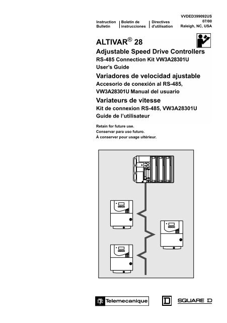
ALTIVAR ® <strong>28</strong><br />
Adjustable Speed Drive Controllers<br />
<strong>RS</strong>-<strong>485</strong> <strong>Connection</strong> <strong>Kit</strong> VW3A<strong>28</strong>301U<br />
User’s Guide<br />
Variadores de velocidad ajustable<br />
Accesorio de conexión al <strong>RS</strong>-<strong>485</strong>,<br />
VW3A<strong>28</strong>301U Manual del usuario<br />
Variateurs de vitesse<br />
<strong>Kit</strong> de connexion <strong>RS</strong>-<strong>485</strong>, VW3A<strong>28</strong>301U<br />
Guide de l’utilisateur<br />
Retain for future use.<br />
Conservar para uso futuro.<br />
À conserver pour usage ultérieur.
52012-012-01<br />
5201201201<br />
<strong>Square</strong> D Company<br />
8001 Hwy 64 East<br />
Knightdale, NC 27545 USA<br />
1-888-<strong>Square</strong>D (1-888-778-2733)<br />
www.squared.com<br />
Electrical equipment should be serviced<br />
only by qualified electrical maintenance<br />
personnel. No responsibility is assumed by<br />
<strong>Square</strong> D for any consequences arising out<br />
of the use of this material.<br />
VVDED399092US 07/00<br />
© 2000 Schneider Electric<br />
All Rights Reserved.<br />
Importado en Mèxico por:<br />
Schneider Electric México, S.A. de C.V.<br />
Calz. J. Rojo Gómez 1121-A<br />
Col. Gpe. del Moral 09300 México, D.F.<br />
Tel. 5804-5000<br />
www.schneider-electric.com.mx<br />
Solamente el personal de mantenimiento<br />
eléctrico especializado deberá prestar<br />
servicios de mantenimiento al equipo<br />
eléctrico. Schneider S.A. no asume<br />
responsabilidad alguna por las<br />
consecuencias emergentes de la<br />
utilización de este material.<br />
VVDED399092US 07/00<br />
© 2000 Schneider Electric<br />
Reservados todos los derechos.<br />
Schneider Canada Inc.<br />
19 Waterman Avenue, M4B 1 Y2<br />
Toronto, Ontario<br />
1-800-565-6699<br />
www.schneider-electric.ca<br />
L’entretien du matériel électrique ne doit<br />
être effectué que par du personnel<br />
qualifié.Schneider S.A. n’assume aucune<br />
responsabilité des conséquences<br />
éventuelles découlant de l’utilisation de ce<br />
matériel.<br />
VVDED399092US 07/00<br />
© 2000 Schneider Electric<br />
Tous droits réservés.
ALTIVAR ® <strong>28</strong> Adjustable Speed Drive<br />
Controllers<br />
<strong>RS</strong>-<strong>485</strong> <strong>Connection</strong> <strong>Kit</strong> VW3A<strong>28</strong>301U<br />
User’s Guide<br />
Variadores de velocidad ajustable ALTIVAR ® <strong>28</strong><br />
Accesorio de conexión al <strong>RS</strong>-<strong>485</strong>, VW3A<strong>28</strong>301U<br />
Manual del usuario<br />
Variateurs de vitesse ALTIVAR ® <strong>28</strong><br />
<strong>Kit</strong> de connexion <strong>RS</strong>-<strong>485</strong>, VW3A<strong>28</strong>301U<br />
Guide de l’utilisateur<br />
© 2000 Schneider Electric All Rights Reserved 1<br />
E<br />
N<br />
G<br />
L<br />
I<br />
S<br />
H<br />
E<br />
S<br />
P<br />
A<br />
Ñ<br />
O<br />
L<br />
F<br />
R<br />
A<br />
N<br />
Ç<br />
A<br />
I<br />
S
E<br />
N<br />
G<br />
L<br />
I<br />
S<br />
H<br />
DANGER<br />
HAZARDOUS VOLTAGE<br />
Read and understand this bulletin in its entirety before installing or<br />
operating ALTIVAR <strong>28</strong> drive controllers. Installation, adjustment,<br />
repair, and maintenance of the drive controllers must be performed<br />
by qualified personnel.<br />
DO NOT short across DC bus capacitors or touch unshielded<br />
components or terminal strip screw connections with voltage<br />
present.<br />
Install and close all covers before applying power or starting the<br />
drive controller.<br />
The user is responsible for conforming to all applicable code<br />
requirements with respect to grounding all equipment.<br />
Many parts in this drive controll er, including printed wiring boards,<br />
operate at line voltage. DO NOT TOUCH. Use only electrically<br />
insulated tools.<br />
Before servicing the drive controller:<br />
Disconnect all power.<br />
Place a “DO NOT TURN ON” label on the drive controller<br />
disconnect.<br />
Lock disconnect in the open position.<br />
Electrical shock will result in death or serious injury.<br />
2 © 2000 Schneider Electric All Rights Reserved
Bulletin No. VVDED399092US ATV<strong>28</strong> <strong>RS</strong><strong>485</strong> <strong>Connection</strong> <strong>Kit</strong> User’s Guide<br />
07/00 Contents<br />
SECTION 1—HARDWARE SETUP . . . . . . . . . . . . . . . . . . . . . . . . . . . . . . . . . . . . . . . . . . 5<br />
INTRODUCTION . . . . . . . . . . . . . . . . . . . . . . . . . . . . . . . . . . . . . . . . . . . . . . . . . . . . . . . . 5<br />
REVISION LEVEL . . . . . . . . . . . . . . . . . . . . . . . . . . . . . . . . . . . . . . . . . . . . . . . . . . . . . . . 5<br />
ADDITIONAL DOCUMENTATION . . . . . . . . . . . . . . . . . . . . . . . . . . . . . . . . . . . . . . . . . . . 5<br />
INSPECTION . . . . . . . . . . . . . . . . . . . . . . . . . . . . . . . . . . . . . . . . . . . . . . . . . . . . . . . . . . .5<br />
CABLE INSTALLATION . . . . . . . . . . . . . . . . . . . . . . . . . . . . . . . . . . . . . . . . . . . . . . . . . . . 6<br />
CONNECTION TO THE BUS . . . . . . . . . . . . . . . . . . . . . . . . . . . . . . . . . . . . . . . . . . . . . . . 7<br />
Cable Pin-Out . . . . . . . . . . . . . . . . . . . . . . . . . . . . . . . . . . . . . . . . . . . . . . . . . . . . . . . . 7<br />
Wiring Practices for <strong>Connection</strong> to a Multidrop Bus . . . . . . . . . . . . . . . . . . . . . . . . . . . 7<br />
<strong>Connection</strong> Examples . . . . . . . . . . . . . . . . . . . . . . . . . . . . . . . . . . . . . . . . . . . . . . . . . . 9<br />
SECTION 2—MODBUS PROTOCOL . . . . . . . . . . . . . . . . . . . . . . . . . . . . . . . . . . . . . . . 11<br />
DESCRIPTION . . . . . . . . . . . . . . . . . . . . . . . . . . . . . . . . . . . . . . . . . . . . . . . . . . . . . . . . . 11<br />
Exchange Format . . . . . . . . . . . . . . . . . . . . . . . . . . . . . . . . . . . . . . . . . . . . . . . . . . . . 11<br />
MODBUS Frames . . . . . . . . . . . . . . . . . . . . . . . . . . . . . . . . . . . . . . . . . . . . . . . . . . . . 11<br />
ATV<strong>28</strong> Address . . . . . . . . . . . . . . . . . . . . . . . . . . . . . . . . . . . . . . . . . . . . . . . . . . . . . . 11<br />
PRINCIPLE OF COMMUNICATION . . . . . . . . . . . . . . . . . . . . . . . . . . . . . . . . . . . . . . . . 12<br />
Master/Slave Relationship . . . . . . . . . . . . . . . . . . . . . . . . . . . . . . . . . . . . . . . . . . . . . 13<br />
Accessible Data . . . . . . . . . . . . . . . . . . . . . . . . . . . . . . . . . . . . . . . . . . . . . . . . . . . . . 13<br />
Exchanges . . . . . . . . . . . . . . . . . . . . . . . . . . . . . . . . . . . . . . . . . . . . . . . . . . . . . . . . . 14<br />
Control and Supervision . . . . . . . . . . . . . . . . . . . . . . . . . . . . . . . . . . . . . . . . . . . . . . . 14<br />
MODBUS Functions . . . . . . . . . . . . . . . . . . . . . . . . . . . . . . . . . . . . . . . . . . . . . . . . . . 15<br />
Function 03: Read N Output Words (RTU Format) . . . . . . . . . . . . . . . . . . . . . . . . 15<br />
Function 06: Write an Output Word (RTU Format) . . . . . . . . . . . . . . . . . . . . . . . . 16<br />
Function 16: Write N Output Words (RTU Format) . . . . . . . . . . . . . . . . . . . . . . . . 16<br />
Exception Responses (RTU Format) . . . . . . . . . . . . . . . . . . . . . . . . . . . . . . . . . . . . . 17<br />
CRC16 Calculation (RTU Format) . . . . . . . . . . . . . . . . . . . . . . . . . . . . . . . . . . . . . . . 17<br />
MSTR BLOCK . . . . . . . . . . . . . . . . . . . . . . . . . . . . . . . . . . . . . . . . . . . . . . . . . . . . . . . . . 18<br />
Overview of MSTR Block . . . . . . . . . . . . . . . . . . . . . . . . . . . . . . . . . . . . . . . . . . . . . . 18<br />
MSTR Block Structure . . . . . . . . . . . . . . . . . . . . . . . . . . . . . . . . . . . . . . . . . . . . . . . . 18<br />
Inputs . . . . . . . . . . . . . . . . . . . . . . . . . . . . . . . . . . . . . . . . . . . . . . . . . . . . . . . . . . 18<br />
Outputs . . . . . . . . . . . . . . . . . . . . . . . . . . . . . . . . . . . . . . . . . . . . . . . . . . . . . . . . . 18<br />
Top Node Content . . . . . . . . . . . . . . . . . . . . . . . . . . . . . . . . . . . . . . . . . . . . . . . . . 19<br />
Middle Node Content . . . . . . . . . . . . . . . . . . . . . . . . . . . . . . . . . . . . . . . . . . . . . . 19<br />
Bottom Node Content . . . . . . . . . . . . . . . . . . . . . . . . . . . . . . . . . . . . . . . . . . . . . . 20<br />
Read and Write MSTR Operations . . . . . . . . . . . . . . . . . . . . . . . . . . . . . . . . . . . . . . . 20<br />
XMIT FUNCTION BLOCK . . . . . . . . . . . . . . . . . . . . . . . . . . . . . . . . . . . . . . . . . . . . . . . . 21<br />
© 2000 Schneider Electric All Rights Reserved 3<br />
E<br />
N<br />
G<br />
L<br />
I<br />
S<br />
H
E<br />
N<br />
G<br />
L<br />
I<br />
S<br />
H<br />
ATV<strong>28</strong> <strong>RS</strong><strong>485</strong> <strong>Connection</strong> <strong>Kit</strong> User’s Guide Bulletin No. VVDED399092US<br />
Contents 07/00<br />
SECTION 3—CONTROLLING AND MONITORING THE<br />
ATV<strong>28</strong> DRIVE CONTROLLER . . . . . . . . . . . . . . . . . . . . . . . . . . . . . . . . . . . . . . . . . 25<br />
DRIVECOM STANDARD ADAPTED TO THE ATV<strong>28</strong> DRIVE CONTROLLER . . . . . . . . 25<br />
Communication Fault Detection . . . . . . . . . . . . . . . . . . . . . . . . . . . . . . . . . . . . . . . . . 26<br />
Maintaining Communication . . . . . . . . . . . . . . . . . . . . . . . . . . . . . . . . . . . . . . . . . . . . 26<br />
ATV<strong>28</strong> CONTROL MODES . . . . . . . . . . . . . . . . . . . . . . . . . . . . . . . . . . . . . . . . . . . . . . . 26<br />
Hand/Off/Auto (HOA) . . . . . . . . . . . . . . . . . . . . . . . . . . . . . . . . . . . . . . . . . . . . . . . . . 26<br />
Local and Remote . . . . . . . . . . . . . . . . . . . . . . . . . . . . . . . . . . . . . . . . . . . . . . . . . . . . <strong>28</strong><br />
Local (Hand) Control . . . . . . . . . . . . . . . . . . . . . . . . . . . . . . . . . . . . . . . . . . . . . . . <strong>28</strong><br />
Remote (Auto) Control . . . . . . . . . . . . . . . . . . . . . . . . . . . . . . . . . . . . . . . . . . . . . <strong>28</strong><br />
Forced Local . . . . . . . . . . . . . . . . . . . . . . . . . . . . . . . . . . . . . . . . . . . . . . . . . . . . . . . . <strong>28</strong><br />
Communication Principle . . . . . . . . . . . . . . . . . . . . . . . . . . . . . . . . . . . . . . . . . . . . . . 31<br />
SUMMARY OF DRIVECOM STANDARD . . . . . . . . . . . . . . . . . . . . . . . . . . . . . . . . . . . . 32<br />
ALTERNATIVE TO DRIVECOM STATE RING . . . . . . . . . . . . . . . . . . . . . . . . . . . . . . . . 35<br />
SECTION 4— PARAMETER DESCRIPTIONS . . . . . . . . . . . . . . . . . . . . . . . . . . . . . . . . 37<br />
ACCESSING PARAMETE<strong>RS</strong>: AN OVERVIEW . . . . . . . . . . . . . . . . . . . . . . . . . . . . . . . . 38<br />
INDEX OF PARAMETE<strong>RS</strong> . . . . . . . . . . . . . . . . . . . . . . . . . . . . . . . . . . . . . . . . . . . . . . . . 39<br />
CONFIGURATION PARAMETE<strong>RS</strong> (READ AND WRITE) . . . . . . . . . . . . . . . . . . . . . . . . 40<br />
General Configuration Parameters . . . . . . . . . . . . . . . . . . . . . . . . . . . . . . . . . . . . . . . 40<br />
I/O Configuration Parameters . . . . . . . . . . . . . . . . . . . . . . . . . . . . . . . . . . . . . . . . . . . 41<br />
Fault Configuration Parameters . . . . . . . . . . . . . . . . . . . . . . . . . . . . . . . . . . . . . . . . . 43<br />
Adjustment Parameters . . . . . . . . . . . . . . . . . . . . . . . . . . . . . . . . . . . . . . . . . . . . . . . 43<br />
CONTROL PARAMETE<strong>RS</strong> (READ AND WRITE) . . . . . . . . . . . . . . . . . . . . . . . . . . . . . . 45<br />
MONITORING PARAMETE<strong>RS</strong> . . . . . . . . . . . . . . . . . . . . . . . . . . . . . . . . . . . . . . . . . . . . 48<br />
SPECIAL DRIVECOM PARAMETE<strong>RS</strong> (READ AND WRITE) . . . . . . . . . . . . . . . . . . . . . 52<br />
4 © 2000 Schneider Electric All Rights Reserved
Bulletin No. VVDED399092US Section 1—Hardware Setup<br />
07/00 Introduction<br />
SECTION 1—HARDWARE SETUP<br />
INTRODUCTION<br />
REVISION LEVEL<br />
ADDITIONAL DOCUMENTATION<br />
INSPECTION<br />
The VW3A<strong>28</strong>301U communication kit is used to connect an<br />
ALTIVAR ® <strong>28</strong> (ATV<strong>28</strong>) drive controller to a MODBUS ® network.The<br />
communication kit includes a 10 ft (3 m) connection cable equipped with<br />
two connectors:<br />
A 9-pin Sub-D female connector for connection to the bus; and<br />
An RJ45 connector for connection to the ATV<strong>28</strong> drive controller.<br />
The ATV<strong>28</strong> drive controller can receive and respond to data messages.<br />
This data exchange enables a network to access ATV<strong>28</strong> functions such<br />
as:<br />
Remote loading of configuration and adjustment parameters<br />
Command and control<br />
Monitoring<br />
Diagnostics<br />
This is the first release of this manual. The information contained in it is<br />
based on ATV<strong>28</strong> firmware version V1.0 or greater.<br />
For more information about ALTIVAR <strong>28</strong> drive controller functions and<br />
operation, please refer to the Installation Guide supplied with your<br />
controller and user manual VVDED399062US.<br />
After receiving the VW3A<strong>28</strong>301U communication kit, ensure that the part<br />
number printed on the label is the same as that on the packing slip.<br />
© 2000 Schneider Electric All Rights Reserved 5<br />
E<br />
N<br />
G<br />
L<br />
I<br />
S<br />
H
E<br />
N<br />
G<br />
L<br />
I<br />
S<br />
H<br />
Section 1—Hardware Setup Bulletin No. VVDED399092US<br />
Installation 07/00<br />
CABLE INSTALLATION<br />
To install the VW3A<strong>28</strong>301U communication cable, consult Figure 1 and<br />
follow these steps:<br />
1. Remove the plug to access the ATV<strong>28</strong> RJ45 connector.<br />
2. Connect the RJ45 cable connector to the ATV<strong>28</strong> connector.<br />
ATV-<strong>28</strong><br />
RJ45 Connector<br />
2<br />
Figure 1: Cable Installation<br />
6 © 2000 Schneider Electric All Rights Reserved<br />
1<br />
9-Pin Sub-D Connector<br />
Plug
Bulletin No. VVDED399092US Section 1—Hardware Setup<br />
07/00 <strong>Connection</strong> to the Bus<br />
CONNECTION TO THE BUS<br />
Cable Pin-Out<br />
Figure 2 illustrates the pin-out for using <strong>RS</strong>-<strong>485</strong> type communication.<br />
RJ45<br />
D(A)<br />
0V<br />
5<br />
2<br />
10V 7 6<br />
D(B)<br />
3<br />
8<br />
9<br />
9-Pin Sub-D<br />
Female<br />
Figure 2: Cable Pin-Out for <strong>RS</strong>-<strong>485</strong> Communication<br />
Wiring Practices for <strong>Connection</strong> to a Multidrop Bus<br />
3<br />
4<br />
7<br />
When wiring ATV<strong>28</strong> drive controllers equipped with communication<br />
options to a multidrop bus, follow the wiring practices required by national<br />
and local electrical codes in addition to the following:<br />
Use metallic conduit for all drive cont roller wiring. Do not run multidrop<br />
cable and power wiring in the same conduit.<br />
Separate metallic conduit carrying power wiring from metallic conduit<br />
containing the multidrop cable by at least 3 in. (8 cm).<br />
Separate non-metallic conduit or cable trays used to carry power<br />
wiring from metallic conduit containing multidrop cable by at least<br />
12 in. (30.5 cm).<br />
Whenever power wiring and multidrop cable cross, the metallic conduit<br />
and non-metallic conduit or trays must cross at right angles.<br />
For the multidrop cable, use shielded cable with one or two pairs of<br />
twisted conductors. Use the cable recommended for each multidrop<br />
bus system shown. Ground the shield only at one point.<br />
© 2000 Schneider Electric All Rights Reserved 7<br />
E<br />
N<br />
G<br />
L<br />
I<br />
S<br />
H
E<br />
N<br />
G<br />
L<br />
I<br />
S<br />
H<br />
Section 1—Hardware Setup Bulletin No. VVDED399092US<br />
<strong>Connection</strong> to the Bus 07/00<br />
When connecting the ATV<strong>28</strong> controller to the <strong>RS</strong>-<strong>485</strong> bus:<br />
Make connections only to pins 3, 4, 6, and 7 of the 9-pin Sub-D cable<br />
receptacle.<br />
Use a shielded cable with two pairs of twisted conductor. Cables are<br />
available from <strong>Square</strong> D in lengths of:<br />
— 3<strong>28</strong> ft (100 m) TSX-CSA100<br />
— 658 ft (200 m) TSX-CSA200<br />
— 1640 ft (500 m) TSX-CSA500<br />
Connect the communication reference potentials to each other.<br />
Do not exceed maximum line length of 3<strong>28</strong>0 ft (1000 m).<br />
Do not exceed maximum tap- off length of 65 ft (20 m).<br />
Do not connect more than 18 nodes on one bus.<br />
Terminate both ends of the bus with a 120 Ω resistor in series with a<br />
0.001 µf capacitor as shown in Figure 3.<br />
D(A)<br />
D(B)<br />
120 Ω<br />
0.001 µF<br />
Figure 3: Zt Line Terminator<br />
8 © 2000 Schneider Electric All Rights Reserved
Bulletin No. VVDED399092US Section 1—Hardware Setup<br />
07/00 <strong>Connection</strong> to the Bus<br />
<strong>Connection</strong> Examples<br />
Figure 4 shows an example of a simplified connection to a PLC. Figure 5<br />
shows an example of a simplified connection of several ATV<strong>28</strong> drive<br />
controllers to a PC. See Table 1 on page 10 for information on the<br />
connection accessories used in the examples.<br />
ATV<strong>28</strong> Controller ATV<strong>28</strong> Controller<br />
VW3A<strong>28</strong>301U VW3A<strong>28</strong>301U<br />
C3 C3<br />
TSX-SCP CM4030<br />
C4<br />
Note: Physical layer accepting eight drive controllers.<br />
Figure 4: Example of a Simplified <strong>Connection</strong> to a PLC<br />
ATV<strong>28</strong> Controller ATV<strong>28</strong> Controller<br />
VW3A<strong>28</strong>301U<br />
VW3-A8106<br />
X3<br />
X1<br />
C5<br />
C3 C3<br />
C6<br />
X2<br />
Note: Physical layer accepting eight drive controllers.<br />
TSX 3721 001/101<br />
+<br />
TSX SCP114<br />
Figure 5: Example of a Simplified <strong>Connection</strong> of Several ATV<strong>28</strong><br />
Drive Controllers to a PC<br />
© 2000 Schneider Electric All Rights Reserved 9<br />
C2<br />
VW3A<strong>28</strong>301U<br />
ATV<strong>28</strong> Controller<br />
VW3A<strong>28</strong>301U<br />
C1<br />
E<br />
N<br />
G<br />
L<br />
I<br />
S<br />
H
E<br />
N<br />
G<br />
L<br />
I<br />
S<br />
H<br />
Section 1—Hardware Setup Bulletin No. VVDED399092US<br />
<strong>Connection</strong> to the Bus 07/00<br />
Table 1: <strong>Connection</strong> Accessories for a Network<br />
Using <strong>RS</strong>-<strong>485</strong> Electrical Interface<br />
Accessory Description<br />
C1<br />
C2<br />
C3<br />
Figure 6: C3 Connector Pins<br />
9-pin male connector (Phoenix Contact SUBCON 9/M-SH<br />
2761509) with cabling of pins 3, 4, 6, and 7 (4 conductor<br />
shielded cables, 1 mm 2 , 16 AWG max.) and 9-pin, SUB-D male/<br />
female adapter, as shown below:<br />
9-pin female connector (Phoenix Contact SUBCON 9/F-SH<br />
2761499) with cabling of pins 3, 4, 6, and 7 (4 conductor<br />
shielded cables, 1 mm 2 , 16 AWG max.).<br />
Phoenix Contact SUBCON-PLUS M2 2761839 connector with<br />
cabling of pins 3, 4, 6, and 7 (4 conductor shielded cables,<br />
1 mm 2 , 16 AWG max.) and 9-pin SUB-D male/female adapter.<br />
Tap off junction TSX SCA50 (if applicable) with TSX-SCP<br />
C4<br />
CM4030 cable wired in correspondence with the C3 pins. See<br />
Figure 6.<br />
C5 Phoenix Contact box, type PSM-PTK 2760623<br />
C6<br />
TSX-CSA...<br />
Signal C3 connector<br />
pins<br />
D(A)<br />
0V<br />
D(B)<br />
3<br />
4<br />
7<br />
Phoenix Contact male connector type SUBCON 9/M-SH with<br />
wiring for pins 3, 4, and 7 (shielded 4-conductor cable 1 mm 2 ,<br />
16 AWG max.).<br />
Cables for bus sold in 3<strong>28</strong> ft (100 m), 658 ft (200 m), and<br />
1640 ft (500 m) lengths.<br />
TSX-SCA50 terminals<br />
if applicable<br />
4<br />
not connected<br />
5<br />
TSX-SCP CM4030<br />
cable wires<br />
10 © 2000 Schneider Electric All Rights Reserved<br />
1<br />
Green, white rings<br />
White, green rings<br />
Shielding
Bulletin No. VVDED399092US Section 2—MODBUS Protocol<br />
07/00 Description<br />
SECTION 2—MODBUS PROTOCOL<br />
DESCRIPTION<br />
Exchange Format<br />
MODBUS Frames<br />
ATV<strong>28</strong> Address<br />
The MODBUS protocol has the following exchange format:<br />
Speed: 9600 or 19200 bps (configured via the bdr parameter<br />
in the keypad “I-O” menu)<br />
Parity: None<br />
Format: 8 bits plus 1 start bit and 1 stop bit<br />
Figure 7 illustrates the structure of MODBUS RTU frames.<br />
Address Request Data CRC16<br />
Figure 7: MODBUS RTU Structure<br />
The data is transmitted in binary code. CRC16 is a cyclical redundancy<br />
check. See page 17 for more information. The end of the frame is<br />
detected by a silence of more than three characters.<br />
The ATV<strong>28</strong> controller address can range from 1 to 31. To configure the<br />
address, use the keypad “I-O” menu of the drive controller or the test and<br />
commissioning software (catalog no. VW3A<strong>28</strong>104).<br />
© 2000 Schneider Electric All Rights Reserved 11<br />
E<br />
N<br />
G<br />
L<br />
I<br />
S<br />
H
E<br />
N<br />
G<br />
L<br />
I<br />
S<br />
H<br />
Section 2—MODBUS Protocol Bulletin No. VVDED399092US<br />
Principle of Communication 07/00<br />
PRINCIPLE OF COMMUNICATION<br />
MODBUS protocol is a dialog protocol that creates a hierarchical<br />
structure (one master and several slaves). MODBUS protocol enables<br />
the master device to interrogate one or more intelligent slave devices. A<br />
multidrop link connects the master and slave devices.<br />
Two types of dialog are possible between the master and slave devices:<br />
1. The master device talks to a slave device and waits for its response.<br />
2. The master device talks to all slave devices without waiting for a<br />
response (broadcast message).<br />
The slave devices are numbered from 1 to 31. The number 0 is reserved<br />
for broadcasting.<br />
Master<br />
Slave 1 Slave 2 Slave 3<br />
Figure 8: Communication Between Master and Slave Devices<br />
The master device initiates and manages the communication exchanges.<br />
The master device repeats the question when there is an incorrect<br />
exchange, and declares the interrogated slave absent if it receives no<br />
response within a given time. Only one device can transmit on the line at<br />
any time. No slave device can send a message unless it is invited to do<br />
so. No lateral communication (i.e., slave to slave) is possible. The<br />
application software of the master device must therefore be designed to<br />
interrogate one slave and send back data received to another slave.<br />
12 © 2000 Schneider Electric All Rights Reserved
Bulletin No. VVDED399092US Section 2—MODBUS Protocol<br />
07/00 Principle of Communication<br />
Master/Slave Relationship<br />
Accessible Data<br />
Once a slave device has been interrogated, the master must wait until it<br />
receives a response before sending any additional commands. Failure to<br />
follow this method causes communication failures.<br />
MODBUS protocol enables the exchange of data (bits and words)<br />
between a master device and several slave devices and checks these<br />
exchanges. Only words can be exchanged with an ATV<strong>28</strong> controller. In<br />
each drive controller there are two types of data objects, input words and<br />
output words. Input words are read only. Output words can be read or<br />
written. Output words are defined with respect to the master device; they<br />
are command, configuration, and adjustment words to the drive<br />
controller.<br />
User<br />
Transmission<br />
table<br />
Reception<br />
table<br />
Figure 9: Data Flow<br />
Modbus Addressing<br />
Slave 1<br />
Input<br />
words<br />
Output<br />
words<br />
program MasterSlave 2<br />
Slave 3<br />
© 2000 Schneider Electric All Rights Reserved 13<br />
E<br />
N<br />
G<br />
L<br />
I<br />
S<br />
H
E<br />
N<br />
G<br />
L<br />
I<br />
S<br />
H<br />
Section 2—MODBUS Protocol Bulletin No. VVDED399092US<br />
Principle of Communication 07/00<br />
Exchanges<br />
Control and Supervision<br />
The master device initiates data exchanges with a slave by supplying it<br />
with four types of data:<br />
1. The slave address<br />
2. The function required of the slave<br />
3. The data zone (variable depending on the request)<br />
4. The exchange check<br />
The master device waits for the response from the slave device before<br />
transmitting the next message, thus avoiding any conflict on the line.<br />
If the slave device receives an invalid message, it transmits an exception<br />
response to the master device, and the master device decides whether to<br />
repeat the exchange.<br />
ATV-<strong>28</strong><br />
Figure 10: Exchanges Between Master and ATV<strong>28</strong> Controller<br />
14 © 2000 Schneider Electric All Rights Reserved
Bulletin No. VVDED399092US Section 2—MODBUS Protocol<br />
07/00 Principle of Communication<br />
MODBUS Functions<br />
MODBUS functions include main functions for data exchange and<br />
additional functions for diagnostics. Table 2 shows the functions that the<br />
ATV<strong>28</strong> communication option manages. The Read and Write functions<br />
are defined from the point of view of the master.<br />
Table 2: MODBUS Functions<br />
Code Type of Function B [1] Limit Description<br />
03 Read N output words 7 max.<br />
Reads words that the master can write<br />
and read in the slave.<br />
06 Write one output word B N/A Writes a 16 bit output word.<br />
16 Write N output words B 7 max.<br />
Writes words that the master can write<br />
and read in the slave.<br />
1. Functions marked “B” can be broadcast. The message transmitted by the master must<br />
specify slave number=0. A response message is never returned.<br />
The following sections provide details of the data frames used for each of<br />
the MODBUS functions.<br />
Function 03: Read N Output Words (RTU Format)<br />
Query:<br />
Slave No. 03<br />
No. of 1st word<br />
Hi Lo<br />
No. of words<br />
Hi Lo<br />
CRC16<br />
1 byte 1 byte 2 bytes 2 bytes 2 bytes<br />
Response:<br />
Slave<br />
No.<br />
03<br />
No. of<br />
bytes<br />
read<br />
For example, to read words W450–W456 of slave 2 (supervision<br />
parameters), send the following data frame:<br />
The response to this query is:<br />
Value of 1st word Value of last word<br />
Hi Lo . . . . . Hi Lo<br />
CRC16<br />
1 byte 1 byte 1 byte 2 bytes 2 bytes 2 bytes<br />
02 03 01C2 000A CRC16<br />
02 03 14 xxxx . . . . . xxxx CRC16<br />
Value of<br />
W450<br />
Value of<br />
W456<br />
© 2000 Schneider Electric All Rights Reserved 15<br />
E<br />
N<br />
G<br />
L<br />
I<br />
S<br />
H
E<br />
N<br />
G<br />
L<br />
I<br />
S<br />
H<br />
Section 2—MODBUS Protocol Bulletin No. VVDED399092US<br />
Principle of Communication 07/00<br />
Function 06: Write an Output Word (RTU Format)<br />
NOTE: The response is always the same as the query (echo).<br />
Query:<br />
Slave No. 06<br />
Word no.<br />
PF PI<br />
Word values<br />
PF PI<br />
CRC16<br />
1 byte 1 byte 2 bytes 2 bytes 2 bytes<br />
Response:<br />
Slave No. 06<br />
Word no.<br />
PF PI<br />
Word values<br />
PF PI<br />
CRC16<br />
1 byte 1 byte 2 bytes 2 bytes 2 bytes<br />
Function 16: Write N Output Words (RTU Format)<br />
Query:<br />
Slave<br />
No.<br />
10<br />
No. of 1st word<br />
Hi Lo<br />
No. of<br />
words<br />
No. of<br />
bytes<br />
Value of 1st word<br />
Hi Lo . . . .<br />
CRC16<br />
1 byte 1 byte 2 bytes 2 bytes 1 byte 2 bytes 2 bytes<br />
Response:<br />
Slave No. 10<br />
No. of 1st word<br />
Hi Lo<br />
No. of words<br />
Hi Lo<br />
CRC16<br />
1 byte 1 byte 2 bytes 2 bytes 2 bytes<br />
For example, to write values 15 and 400 in words W400 and W401 of<br />
slave 2, you would send the following data frame:<br />
02 10 0190 0002 04 000F 0190 CRC16<br />
The response to this message would be:<br />
02 10 0190 0002 CRC16<br />
16 © 2000 Schneider Electric All Rights Reserved
Bulletin No. VVDED399092US Section 2—MODBUS Protocol<br />
07/00 Principle of Communication<br />
Exception Responses (RTU Format)<br />
CRC16 Calculation (RTU Format)<br />
A slave returns an exception response when it is unable to perform the<br />
request addressed to it. The format of an exception response is as<br />
follows:<br />
Slave No. Response Code Error Code CRC16<br />
1 byte 1 byte 1 byte 2 bytes<br />
Response code Function code of the request + H'80' (the most significant bit is set to 1)<br />
Error Code<br />
1 = The slave does not recognize the function requested.<br />
2 = The bit and word numbers (addresses) indicated in the request do not<br />
exist in the slave.<br />
3 = The bit and word values indicated in the request are not accessible in<br />
the slave.<br />
4 = The slave has started to execute the request but cannot continue to<br />
process it completely.<br />
The CRC16 is calculated on all the bytes of the message by applying the<br />
following method ('XOR' indicates Exclusive-Or):<br />
Initialize the CRC (16-bit register) to H'FFFF.<br />
Enter the first to the la st byte of the message:<br />
CRC XOR →CRC<br />
ENTER 8 times<br />
Move the CRC one bit to the right<br />
If the output bit = 1, enter CRC XOR H'A001 →CRC<br />
END enter<br />
The low order bytes of the CRC obtained are transmitted first, then the<br />
high order ones.<br />
© 2000 Schneider Electric All Rights Reserved 17<br />
E<br />
N<br />
G<br />
L<br />
I<br />
S<br />
H
E<br />
N<br />
G<br />
L<br />
I<br />
S<br />
H<br />
Section 2—MODBUS Protocol Bulletin No. VVDED399092US<br />
MSTR Block 07/00<br />
MSTR BLOCK<br />
Overview of MSTR Block<br />
MSTR Block Structure<br />
A network of <strong>28</strong> drive controllers using <strong>RS</strong>-<strong>485</strong> can be created using the<br />
MSTR block and a MODBUS PLUS to MODBUS converter.This section<br />
discusses read and write MSTR instruction blocks. For additional<br />
information on MODBUS instructions, refer to the Modicon Ladder Logic<br />
Block Library User Guide, 840 USE 10100.<br />
PLCs that support MODBUS PLUS communications have a special<br />
MSTR (master) instruction allowing nodes of the network to initiate<br />
message transactions. The MSTR function allows you to initiate one of<br />
nine possible network communications operations over the MODBUS<br />
PLUS network. Each operation is designated by a code (see Table 3).<br />
Table 3: MSTR Operation Codes<br />
MSTR Operation Code MSTR Operation Code<br />
Write Data 1 Read Global Database 6<br />
Read Data 2 Get Remote Statistics 7<br />
Get Local Statistics 3 Clear Remote Statistics 8<br />
Write Global Database 5 Peer Cop Status 9<br />
Inputs<br />
MSTR has two control points (see Figure 11 on page 19):<br />
Top node input—enables the instruction when it is ON.<br />
Middle node input—terminates the active operation when it is ON.<br />
Outputs<br />
MSTR can produce three possible outputs (see Figure 11):<br />
Top node output—echoes the state of the top input (goes ON while the<br />
instruction is active).<br />
Middle node output—echoes the stat e of the middle input and goes<br />
ON if the MSTR operation is terminated prior to completion.<br />
Bottom node output—goes ON when an MSTR operation is completed<br />
successfully.<br />
18 © 2000 Schneider Electric All Rights Reserved
Bulletin No. VVDED399092US Section 2—MODBUS Protocol<br />
07/00 MSTR Block<br />
Enables selected<br />
MSTR operation<br />
Terminates active<br />
MSTR operation<br />
Figure 11: MSTR Block Structure<br />
Top Node Content<br />
The 4x register entered in the top node is the first of nine contiguous<br />
holding registers that comprise the control block (see Table 4).<br />
Table 4: Control Block Holding Registers<br />
Register Content<br />
Displayed Identifies one of the nine MSTR operations<br />
1st implied Displays error status<br />
2nd implied Displays length<br />
3rd implied Displays MSTR operation-dependent information<br />
4th implied<br />
Routing 1 register, used to designate the address of the destination<br />
node for a network message transaction.<br />
5th implied Routing 2 register<br />
6th implied Routing 3 register<br />
7th implied Routing 4 register<br />
8th implied Routing 5 register<br />
Middle Node Content<br />
Control<br />
Block<br />
Data<br />
Area<br />
MSTR<br />
Length<br />
Operation active<br />
Operation terminated<br />
unsuccessfully<br />
Operation successful<br />
The 4x register entered in the middle node is the first in a group of<br />
contiguous holding registers that comprise the data area. For operations<br />
that provide the communication processor with data—such as a write<br />
operation—the data area is the source of the data. For operations that<br />
acquire data from the communication processor—such as a read<br />
operation—the data area is the destination for the data.<br />
© 2000 Schneider Electric All Rights Reserved 19<br />
E<br />
N<br />
G<br />
L<br />
I<br />
S<br />
H
E<br />
N<br />
G<br />
L<br />
I<br />
S<br />
H<br />
Section 2—MODBUS Protocol Bulletin No. VVDED399092US<br />
MSTR Block 07/00<br />
Bottom Node Content<br />
Read and Write MSTR Operations<br />
The integer value entered in the bottom node specifies the length—the<br />
maximum number of registers—in the data area. Although the typical<br />
MODBUS length can range from 1 to 100, the ATV<strong>28</strong> drive controller<br />
range is 1 to 60.<br />
An MSTR write operation transfers data from a controlling device to the<br />
drive controller. An MSTR read operation transfers data from the drive<br />
controller to a controlling device on the network.<br />
The registers in the MSTR control block (the top node) contain the<br />
following information in a read or write operation (see Table 5).<br />
Table 5: Control Block Registers—Read and Write Operations<br />
Register Function Content<br />
Displayed Operation type 1 = Write; 2 = Read<br />
1st implied Error status Displays a hex value indicating MSTR error, when relevant<br />
2nd implied Length<br />
3rd implied<br />
4th … 8th<br />
implied<br />
Drive controller<br />
data area<br />
Routing 1 … 5<br />
Write = # of registers to be sent to drive controller<br />
Read = # of registers to be read from drive controller<br />
Specifies starting register in the drive controller to be read<br />
from or written to<br />
Designates 1st … 5th routing path addresses, respectively;<br />
last non-zero byte in routing path is the transaction device.<br />
20 © 2000 Schneider Electric All Rights Reserved
Bulletin No. VVDED399092US Section 2—MODBUS Protocol<br />
07/00 XMIT Function Block<br />
XMIT FUNCTION BLOCK<br />
The XMIT function block allows you to make a MODBUS port a master<br />
on various Modicon PLCs. See Figure 12 for an example of a XMIT<br />
function block on a ProWork Nxt screen. Consult the appropriate Modicon<br />
documentation to ensure that your configuration and options allow the<br />
MODBUS port to be modified.<br />
NOTE: The MODBUS/JBUS/UNITELWAY communication option card<br />
uses a two-wire <strong>RS</strong>-<strong>485</strong> electrical interface. If the port you are using on<br />
the PLC is an <strong>RS</strong>-232 interface that does not support <strong>RS</strong>-<strong>485</strong>, you must<br />
use an <strong>RS</strong>-232 to <strong>RS</strong>-<strong>485</strong> converter that is Auto enabled (sometimes<br />
called Data enabled). Remember that some ports are only <strong>RS</strong>-422 and<br />
require an <strong>RS</strong>-422 to <strong>RS</strong>-<strong>485</strong> converter.<br />
Figure 12: XMIT Function Block<br />
© 2000 Schneider Electric All Rights Reserved 21<br />
E<br />
N<br />
G<br />
L<br />
I<br />
S<br />
H
E<br />
N<br />
G<br />
L<br />
I<br />
S<br />
H<br />
Section 2—MODBUS Protocol Bulletin No. VVDED399092US<br />
XMIT Function Block 07/00<br />
The XMIT instruction block (shown in Figure 13) lets you transmit data<br />
directly out of the PLC. You can set the parity, stop bits, and pulse or tone<br />
dialing (among other values) just like a modem.<br />
Start XMIT<br />
operation<br />
Abort XMIT<br />
operation<br />
#0001<br />
4xxxx<br />
XMIT<br />
#0016<br />
Operation is active<br />
Figure 13: XMIT Instruction Block<br />
Operation terminated<br />
unsuccessfully<br />
Operation successful<br />
#0001: The top node must contain the constant #0001.<br />
4xxxx: The 4x register in the middle node addresses the first in a<br />
group of 16 contiguous registers that comprise the control block.<br />
#0016: The bottom node must contain the constant #0016. This is the<br />
number of registers in the control block pointed to by the middle node.<br />
Start XMIT operation: Begins an XMIT operation. Your logic should<br />
keep this on until the operation completes successfully or an error<br />
occurs.<br />
Abort XMIT operation: Aborts an active XMIT operation, forcing the<br />
port to slave mode. The abort code 121 is placed in the fault status<br />
register. The port remains closed as long as this input is on.<br />
Operation is active: Passes power while an XMIT operation is in<br />
progress.<br />
Operation terminated unsuccessfully: Passes power when XMIT<br />
has detected an error or when an XMIT operation was aborted.<br />
Operation successful: Passes power when an XMIT operation has<br />
successfully completed.<br />
NOTE: Do not modify the address in the 4xxxx middle node or delete<br />
XMIT from the program while the block is active. This locks up the<br />
communication port, preventing further communication.<br />
22 © 2000 Schneider Electric All Rights Reserved
Bulletin No. VVDED399092US Section 2—MODBUS Protocol<br />
07/00 XMIT Function Block<br />
The XMIT instruction block does not operate correctly if:<br />
The NSUP and XMIT loadable are not installed.<br />
The NSUP loadable is installed after the XMIT loadable.<br />
The NSUP and XMIT loadables are installed in a Quantum PLC with<br />
an out-of-date executive (older than version 2.10 or 2.12).<br />
Registers in the XMIT control block are as follows:<br />
Table 6: XMIT Control Block Registers<br />
Register Function Range<br />
4x Revision Number Read only. Decimal.<br />
4x+1 Fault Status Read only.<br />
4x+2 Not used by XMIT Available for customer use.<br />
4x+3 Data Rate<br />
50, 75, 110, 134, 150, 300, 600, 1200,<br />
2400, 9600, or 19200 bits per second.<br />
4x+4 Data Bits 7, 8<br />
4x+5 Parity 0, 1, 2<br />
4x+6 Stop Bits 0, 1, 2<br />
4x+7 Not used by XMIT Available for customer use.<br />
4x+8 Command Word 16-digit binary number.<br />
4x+9 Pointer to Message Table<br />
Values are limited by the range of 4x<br />
registers configured.<br />
4x+10 Length of Message 0–512<br />
4x+11 Response Time-out 0–65535 milliseconds<br />
4x+12 Retry Limit 0–65535 milliseconds<br />
4x+13 Start of Transmission Delay 0–65535 milliseconds<br />
4x+14 End of Transmission Delay 0–65535 milliseconds<br />
4x+15 Current Retry Read only.<br />
The MSTR and XMIT functions have the ability to violate the MODBUS<br />
Master/Slave architecture, as does a custom-written MODBUS driver.<br />
A communication request must not be issued before the previous<br />
request has been completed. Otherwise, the communication<br />
requests can cause the drive controller’s memory to overflow,<br />
resulting in a communication fault.<br />
© 2000 Schneider Electric All Rights Reserved 23<br />
E<br />
N<br />
G<br />
L<br />
I<br />
S<br />
H
E<br />
N<br />
G<br />
L<br />
I<br />
S<br />
H<br />
Section 2—MODBUS Protocol Bulletin No. VVDED399092US<br />
XMIT Function Block 07/00<br />
NOTES<br />
24 © 2000 Schneider Electric All Rights Reserved
Bulletin No. VVDED399092US Section 3—Controlling and Monitoring the ATV<strong>28</strong> Drive Controller<br />
07/00 DRIVECOM Standard Adapted to the ATV<strong>28</strong> Controller<br />
SECTION 3—CONTROLLING AND MONITORING THE ATV<strong>28</strong> DRIVE<br />
CONTROLLER<br />
DRIVECOM STANDARD ADAPTED TO THE ATV<strong>28</strong> DRIVE CONTROLLER<br />
The ATV<strong>28</strong> control process using the serial link conforms to the<br />
DRIVECOM standard state chart. Figure 16 illustrates the DRIVECOM<br />
standard adapted to the characteristics of the ATV<strong>28</strong> drive controller to<br />
facilitate programming. Each state represents an aspect of the internal<br />
behavior of the drive controller.<br />
The drive controller status can be modified by sending control word CMD<br />
(word W400), a hexadecimal value, or by the occurrence of an event such<br />
as a drive controller lock after a fault. The drive controller status is<br />
indicated by the value of the status register (ETA).<br />
When a fault occurs, ETA (word 458) is set to xxx8h. To clear the fault, set<br />
CMD (word 400) to a value of 80h. The drive controller is now on and<br />
locked, with ETA set to a value of xx40h. To enter “Standby Status”, write<br />
“0006h” to CMD. ETA now has a value of xx21h. Next, enter the “Ready”<br />
state by writing “0007h” to CMD. ETA now has a value of xx23h. At this<br />
point, the motor can be commanded to rotate forward (by writing “000Fh”<br />
to CMD) or reverse (by writing “080Fh” to CMD).<br />
© 2000 Schneider Electric All Rights Reserved 25<br />
E<br />
N<br />
G<br />
L<br />
I<br />
S<br />
H
E<br />
N<br />
G<br />
L<br />
I<br />
S<br />
H<br />
Section 3—Controlling and Monitoring the ATV<strong>28</strong> Drive Controller Bulletin No. VVDED399092US<br />
ATV<strong>28</strong> Control Modes 07/00<br />
Communication Fault Detection<br />
Maintaining Communication<br />
ATV<strong>28</strong> CONTROL MODES<br />
Hand/Off/Auto (HOA)<br />
WARNING<br />
LOSS OF CONTROL<br />
Provide some method of controlling the drive controller until<br />
communication is established. Provide alternate control paths (Start,<br />
Stop, and Speed):<br />
When disabling communication loss detection.<br />
When motor control is required while a communication fault exists.<br />
Failure to follow these instructions can result in death, serious<br />
injury, or equipment damage.<br />
Setting CMI (word W402) bit 14 to 1 disables communication loss<br />
detection. As a result, loss of communication does not cause the drive<br />
controller to generate a fault. The drive controller continues its present<br />
operation. Alternate control paths must be provided for starting, stopping,<br />
and controlling the motor. No control commands are received during loss<br />
of communication. This function is intended for use during<br />
troubleshooting and start-up.<br />
After communication has been established, the drive controller must<br />
receive a communication request (read or write) every seven seconds or<br />
the drive controller will generate a communication fault. A<br />
communication request must not be issued before the previous<br />
request has been completed. Otherwise, the communication<br />
requests can cause the drive controller’s memory to overflow,<br />
resulting in a communication fault.<br />
If a communication fault is generated, the fault prevents starting the<br />
controlled motor until the fault is cleared. Recycling the power clears the<br />
fault.<br />
When the ATV<strong>28</strong> drive controller is powered up, it defaults to local (hand)<br />
control. See the discussion of local and remote control on page <strong>28</strong>. After<br />
the drive controller recovers from a power up sequence (including such<br />
unplanned events as an AC line power disturbance), it immediately<br />
responds to local controls that may be active before the MODBUS<br />
26 © 2000 Schneider Electric All Rights Reserved
Bulletin No. VVDED399092US Section 3—Controlling and Monitoring the ATV<strong>28</strong> Drive Controller<br />
07/00 ATV<strong>28</strong> Control Modes<br />
communication link has initialized and assumed control of the drive<br />
controller. This results in unintended equipment operation. It is<br />
therefore required that all local (hand) run and start commands to<br />
the drive controller be removed when the system is in the remote<br />
(auto) mode.<br />
While it is possible to stop the drive controller in remote (auto) mode by<br />
activating one of the local stop commands (such as the keypad display<br />
stop button), commands sent over the MODBUS link can restart the drive<br />
controller if the drive controller is not in a forced local condition. See the<br />
discussion of forced local on <strong>28</strong>. It is therefore necessary to put the<br />
drive controller into the forced local mode when the control switch<br />
is in the hand or off position.<br />
LOSS OF CONTROL<br />
The user must provide a Hand/Off/Auto switch with the following<br />
functionality:<br />
In Hand mode, forced local must be enabled.<br />
In Off mode, all run terminal inputs must be disabled via open<br />
circuit and forced local must be enabled.<br />
In Auto mode, the run terminal inputs must be disabled via open<br />
circuit and forced local must be disabled.<br />
Failure to follow these instructions can result in death or serious<br />
injury.<br />
See Figures 14 and 15 for assistance in designing Hand/Off/Auto control.<br />
User<br />
Control<br />
Scheme<br />
Hand Off Auto<br />
WARNING<br />
Figure 14: Example 2-Wire Control<br />
LI1 Run Forward<br />
© 2000 Schneider Electric All Rights Reserved 27<br />
+24<br />
LI2 Run Reverse<br />
LI3 Forced Local<br />
E<br />
N<br />
G<br />
L<br />
I<br />
S<br />
H
E<br />
N<br />
G<br />
L<br />
I<br />
S<br />
H<br />
Section 3—Controlling and Monitoring the ATV<strong>28</strong> Drive Controller Bulletin No. VVDED399092US<br />
ATV<strong>28</strong> Control Modes 07/00<br />
Local and Remote<br />
Forced Local<br />
NOTE: Removal of local Run Forward or Run Reverse commands while<br />
the HOA switch is in the Auto position will not stop the drive controller.<br />
Stop<br />
Fwd Rev<br />
Figure 15: Example 3-Wire Control<br />
The ATV<strong>28</strong> drive controller can be commanded in local and remote<br />
control modes.<br />
Local (Hand) Control<br />
The drive is controlled by operators such as push buttons, switches,<br />
and a speed potentiometer that are wired to the drive controller<br />
terminal block or<br />
The drive is controlled by the digital keypad display buttons.<br />
See the ATV<strong>28</strong> User’s Guide, VVDED399062US, for more details on how<br />
to select between the two modes of local control.<br />
Remote (Auto) Control<br />
Hand Off Auto<br />
The drive is controlled by the MODBUS serial link.<br />
The speed reference and the start/stop control cannot come from<br />
separate sources.<br />
Switching between local and remote control is achieved by a switch wired<br />
to a logic input on the controller terminal block as illustrated in Figures 14<br />
(page 27) and 15. The logic input must be assigned to the function<br />
“Forced Local.”<br />
<strong>28</strong> © 2000 Schneider Electric All Rights Reserved<br />
+24<br />
LI1 Stop<br />
LI2 Run Forward<br />
LI3 Run Reverse<br />
LI4 Forced Local
Bulletin No. VVDED399092US Section 3—Controlling and Monitoring the ATV<strong>28</strong> Drive Controller<br />
07/00 ATV<strong>28</strong> Control Modes<br />
When the logic input assigned to forced local is active (high), all control<br />
of the drive is assigned to the selected local (hand) control mode. In this<br />
case, command requests by the MODBUS network are refused.<br />
Command parameters can be monitored. All other parameters may be<br />
read/write accessed.<br />
WARNING<br />
UNINTENDED EQUIPMENT ACTION<br />
When in forced local mode, all commands from the communication<br />
ports are ignored.<br />
Failure to consider the implications of unanticipated operation<br />
can result in death, serious injury, or equipment damage.<br />
When the logic input is not active (low), all control of the drive is<br />
transferred to the MODBUS network. The only local (hand) controls that<br />
are still monitored by the drive controller include the logic input assigned<br />
to Forced Local and any input assigned to a drive stop function. Examples<br />
include the stop button on the keypad display, logic input 1 (LI1)—which<br />
is assigned to the function STOP if the ATV<strong>28</strong> drive controller is<br />
configured for 3-wire control—and any logic input assigned to the<br />
functions freewheel stop, DC injection braking, and fast stop.<br />
See the ATV<strong>28</strong> Drive Controller User’s Guide, VVDED399062US (latest<br />
revision), for more details.<br />
© 2000 Schneider Electric All Rights Reserved 29<br />
E<br />
N<br />
G<br />
L<br />
I<br />
S<br />
H
E<br />
N<br />
G<br />
L<br />
I<br />
S<br />
H<br />
Section 3—Controlling and Monitoring the ATV<strong>28</strong> Drive Controller Bulletin No. VVDED399092US<br />
ATV<strong>28</strong> Control Modes 07/00<br />
No malfunction<br />
& com. reg. =<br />
DISABLE<br />
VOLTAGE<br />
9<br />
No malfunction<br />
& com. reg. =<br />
SHUT DOWN<br />
8<br />
No malfunction<br />
0<br />
Not operable<br />
xx00h<br />
1<br />
No malfunction<br />
& com. reg. =<br />
SHUT<br />
DOWN<br />
2<br />
No malfunction<br />
& power<br />
present<br />
& com. reg. =<br />
SWITCH ON<br />
3<br />
15<br />
Switch ON<br />
Disabled<br />
xx40h<br />
Ready to Switch<br />
ON<br />
xx21h<br />
Switched ON<br />
xx23h<br />
No malfunction<br />
& com. reg. =<br />
DISABLE<br />
VOLTAGE or<br />
QUICK STOP<br />
7<br />
No malfunction<br />
& com. reg. =<br />
SHUT DOWN<br />
6<br />
Malfunction 13<br />
No malfunction<br />
& com. reg. = RESET<br />
MALFUNCTION<br />
Malfunction 13<br />
12<br />
Malfunction 13<br />
No malfunction<br />
& com. reg. =<br />
DISABLE<br />
VOLTAGE or<br />
QUICK STOP<br />
10<br />
Malfunction 13<br />
Figure 16: DRIVECOM as Implemented on the<br />
ATV<strong>28</strong> Drive Controller<br />
Malfunction<br />
Reaction active<br />
xxxFh<br />
Malfunction<br />
xxx8h<br />
Malfunction<br />
No malfunction<br />
& com. reg. =<br />
DISABLE<br />
VOLTAGE<br />
No malfunction<br />
& com. reg. =<br />
ENABLE<br />
OPERATION<br />
No malfunction<br />
& com. reg. =<br />
DISABLE<br />
OPERATION<br />
13<br />
4 5<br />
Malfunction<br />
Operation<br />
Malfunction Quick Stop<br />
Enabled<br />
Active<br />
xx27h<br />
11 NOTE: Italics indicate transition xx07h names<br />
No malfunction and numbers from the DRIVECOM<br />
& com. reg. = QUICK Standard shown in Figure 17 on page<br />
New com. reg.<br />
l<br />
STOP 34.<br />
30 © 2000 Schneider Electric All Rights Reserved<br />
14
Bulletin No. VVDED399092US Section 3—Controlling and Monitoring the ATV<strong>28</strong> Drive Controller<br />
07/00 ATV<strong>28</strong> Control Modes<br />
Communication Principle<br />
Table 7: STOP Requests<br />
Type of Stop<br />
Corresponding<br />
DRIVECOM state<br />
Freewheel stop ATV<strong>28</strong> powered up<br />
Fast stop ATV<strong>28</strong> running<br />
DC injection stop ATV<strong>28</strong> running<br />
Stop via keypad STOP key ATV<strong>28</strong> powered up<br />
3-wire control stop via logic<br />
input stop (LI1)<br />
ATV<strong>28</strong> powered up<br />
To restore control of the<br />
ATV<strong>28</strong> drive controller<br />
using the fieldbus:<br />
1. Set the terminal strip logic input<br />
assigned to the freewheel stop<br />
function to 1.<br />
2. Perform the transitions required to<br />
return the drive controller to “Run”<br />
status.<br />
Set the terminal strip logic input<br />
assigned to the fast stop function to 1.<br />
Set the terminal strip logic input<br />
assigned to the DC injection stop<br />
function to 0.<br />
1. Release the Stop key.<br />
2. Perform the transitions required to<br />
return the drive controller to “Run”<br />
status.<br />
1. Set the logic input assigned to<br />
STOP to 1.<br />
2. Perform the transitions required to<br />
return the drive controller to “Run”<br />
status.<br />
The ATV<strong>28</strong> drive controller can be connected to only one fieldbus, and<br />
this one fieldbus controls the ATV<strong>28</strong>.<br />
The fieldbus connected to the communication port always takes priority.<br />
However, when the MODBUS master is not controlling the ATV<strong>28</strong>, the<br />
fieldbus may send configuration words (provided the motor is stopped),<br />
adjustments, and read display words.<br />
The bus controlling the drive controller can relinquish control by setting<br />
bits 8 and 15 of the control word 400 (CMD) to 1.<br />
For further information, refer to the communication principles described<br />
on page 13.<br />
© 2000 Schneider Electric All Rights Reserved 31<br />
E<br />
N<br />
G<br />
L<br />
I<br />
S<br />
H
E<br />
N<br />
G<br />
L<br />
I<br />
S<br />
H<br />
Section 3—Controlling and Monitoring the ATV<strong>28</strong> Drive Controller Bulletin No. VVDED399092US<br />
Summary of DRIVECOM Standard 07/00<br />
SUMMARY OF DRIVECOM STANDARD<br />
Table 8: Control Register (CMD) Bit Definition [1]<br />
bit 0 bit 1 bit 2 bit 3 bit 4 bit 5 bit 6 bit 7<br />
Switch ON Disable<br />
voltage<br />
Switch to<br />
drive<br />
controller<br />
ready<br />
Return to<br />
ATV<strong>28</strong><br />
powered<br />
up status<br />
Quick stop Enable<br />
operation<br />
optional optional optional<br />
Fast stop Run/stop reserved reserved reserved<br />
bit 8 bit 9 bit 10 bit 11 bit 12 bit 13 bit 14 bit 15<br />
reserved reserved reserved<br />
reserved reserved reserved<br />
specific to<br />
manufacturer<br />
Reverse<br />
motor<br />
direction<br />
specific to<br />
manufacturer<br />
reserved<br />
specific to<br />
manufacturer<br />
Stop by<br />
injection<br />
specific to<br />
manufacturer<br />
Reset<br />
malfunction<br />
Reset fault<br />
acknowledged<br />
specific to<br />
manufacturer<br />
Fast stop see page 35<br />
[1] The grey boxes correspond to the DRIVECOM standard. The white boxes correspond to the adaptation of<br />
the ATV<strong>28</strong> controller to this standard. See also Table 20 on page 46.<br />
Table 9: Control Register Commands<br />
DRIVECOM<br />
command shown in<br />
Figure 17 on page 34<br />
initial/default state<br />
Switch ON disabled<br />
bit 7 bit 3 bit 2 bit 1 bit 0<br />
transition in DRIVECOM<br />
diagram (see Figure 16 on page<br />
30 or Figure 17 on page 34)<br />
1 0 0 0 0 1 00F0H<br />
Shut Down X X 1 1 0 2, 6, 8 0006h<br />
Switch ON X X 1 1 1 3 0007h<br />
Disable Voltage X X X 0 X 7, 9, 10, 12 0000h<br />
Quick Stop X X 0 1 X 11 000Bh<br />
Disable Operation X 0 1 1 1 5 0007h<br />
Enable Operation X 1 1 1 1 4 000Fh<br />
Reset Malfunction 0>1 X X X X 15 0080h<br />
X: State is not significant<br />
0>1: Rising edge (switch from 0 to 1)<br />
sample values of<br />
the control register<br />
32 © 2000 Schneider Electric All Rights Reserved
Bulletin No. VVDED399092US Section 3—Controlling and Monitoring the ATV<strong>28</strong> Drive Controller<br />
07/00 Summary of DRIVECOM Standard<br />
Table 10: Status Register (ETA) Bit Definition [1]<br />
bit 0 bit 1 bit 2 bit 3 bit 4 bit 5 bit 6 bit 7<br />
Ready to<br />
switch ON<br />
not ready/<br />
ready for<br />
start-up<br />
Switched<br />
ON<br />
drive<br />
controller<br />
not ready/<br />
ready<br />
Operation<br />
enabled<br />
stop/run<br />
Malfunction<br />
no<br />
malfunction<br />
Voltage<br />
disabled<br />
power on/off<br />
Quick stop<br />
fast stop in<br />
progress<br />
Switch ON<br />
disabled<br />
drive<br />
controller<br />
locked<br />
Warning<br />
Alarm<br />
bit 8 bit 9 bit 10 bit 11 bit 12 bit 13 bit 14 bit 15<br />
Message Remote<br />
reserved<br />
local/<br />
remote<br />
Reference<br />
reached<br />
reference<br />
reached<br />
Limit value reserved reserved<br />
min. or max.<br />
reserved reserved<br />
value reached<br />
specific to<br />
manufacturer<br />
stop via STOP<br />
key<br />
specific to<br />
manufacturer<br />
direction of<br />
rotation<br />
forward/reverse<br />
[1] Grey boxes correspond to the DRIVECOM standard. White boxes correspond to the adaptation of the ATV<strong>28</strong><br />
controller to this standard. See also W458 on page 49.<br />
Table 11: Status Register (ETA) States<br />
State in DRIVECOM Standard shown in<br />
Figure 17 on page 34<br />
bit 6 bit 5 bit 3 bit 2 bit 1 bit 0<br />
Not ready to switch ON 0 X 0 0 0 0<br />
Switch ON disabled 1 X 0 0 0 0<br />
Ready to switch ON 0 1 0 0 0 1<br />
Switch ON 0 1 0 0 1 1<br />
Operation enabled 0 1 0 1 1 1<br />
Malfunction 0 X 1 0 0 0<br />
Malfunction Reset Active 0 X 1 1 1 1<br />
Quick stop active<br />
X: State is not significant<br />
0 0 0 1 1 1<br />
Bit 4 is not significant and is therefore not shown in the table.<br />
Table 12: Description of Other Status Register (ETA) Bits<br />
bit 4 Supply voltage = 1 Power is absent<br />
bit 7 Warning = 1 A standard or user-specific warning is present<br />
bit 8 Message = 1 A message (event) is present (optional)<br />
bit 9 Remote = 1 If the parameters can be modified via bus outside local forcing<br />
bit 10 Reference reached = 1 If the reference value is reached<br />
bit 11 Limit value = 1 If a limit value is reached (min-max speed)<br />
© 2000 Schneider Electric All Rights Reserved 33<br />
E<br />
N<br />
G<br />
L<br />
I<br />
S<br />
H
E<br />
N<br />
G<br />
L<br />
I<br />
S<br />
H<br />
Section 3—Controlling and Monitoring the ATV<strong>28</strong> Drive Controller Bulletin No. VVDED399092US<br />
Summary of DRIVECOM Standard 07/00<br />
No malfunction<br />
& com. reg. =<br />
DISABLE<br />
VOLTAGE<br />
9<br />
No malfunction<br />
& com. reg. =<br />
SHUT DOWN<br />
8<br />
No malfunction<br />
0<br />
Not operable<br />
xx00h<br />
1<br />
No malfunction<br />
& com. reg. =<br />
SHUT<br />
DOWN<br />
2<br />
No malfunction<br />
& power<br />
present<br />
& com. reg. =<br />
SWITCH ON<br />
3<br />
15<br />
Switch ON<br />
Disabled<br />
xx40h<br />
Ready to Switch<br />
ON<br />
xx21h<br />
Operation<br />
Enabled<br />
xx27h<br />
No malfunction<br />
& com. reg. =<br />
DISABLE<br />
VOLTAGE or<br />
QUICK STOP<br />
7<br />
No malfunction<br />
& com. reg. =<br />
SHUT DOWN<br />
6<br />
Malfunction 13<br />
No malfunction<br />
& com. reg. = RESET<br />
MALFUNCTION<br />
Malfunction 13<br />
12<br />
Malfunction 13<br />
No malfunction<br />
& com. reg. =<br />
DISABLE<br />
VOLTAGE or<br />
QUICK STOP<br />
10<br />
Switched ON<br />
xx23h<br />
Malfunction 13<br />
No malfunction<br />
& com. reg. =<br />
ENABLE<br />
OPERATION<br />
No malfunction<br />
& com. reg. =<br />
DISABLE<br />
OPERATION<br />
4 5<br />
Malfunction<br />
New com. reg.<br />
value or<br />
Speed Reference Value<br />
11<br />
No malfunction<br />
& com. reg. = QUICK<br />
STOP<br />
Figure 17: DRIVECOM Standard<br />
Malfunction<br />
Reaction active<br />
xxxFh<br />
Malfunction<br />
xxx8h<br />
No malfunction<br />
& com. reg. =<br />
DISABLE<br />
VOLTAGE<br />
Quick Stop<br />
Active<br />
xx07h<br />
34 © 2000 Schneider Electric All Rights Reserved<br />
13<br />
Malfunction<br />
14<br />
Malfunction
Bulletin No. VVDED399092US Section 3—Controlling and Monitoring the ATV<strong>28</strong> Drive Controller<br />
07/00 Alternative to DRIVECOM State Ring<br />
ALTERNATIVE TO DRIVECOM STATE RING<br />
The drivecom state ring can be bypassed by setting the following bits in<br />
W400 CMD:<br />
By setting bits 15, 3, and 1 to a “1” (800A Hex, 32778 Decimal), the<br />
drive controller runs at the frequency reference.<br />
By setting bits 15, 12, 3, and 1 to a “1” (900A Hex, 36874 Decimal), the<br />
drive controller stops the motor on the programmed deceleration ramp.<br />
By setting bits 15, 13, 3, and 1 to a “1” (A00A Hex, 40970 Decimal),<br />
the drive controller stops the motor using the DC injection settings.<br />
By setting bits 15, 14, 3, and 1 to a “1” C00A Hex, 49162 Decimal), the<br />
drive controller fast stops using the Fast Stop settings.<br />
By setting bits 15, 11, 3, and 1 to a “1” (880A Hex, 34826 Decimal), the<br />
drive controller runs in the reverse direction at the frequency<br />
reference.<br />
© 2000 Schneider Electric All Rights Reserved 35<br />
E<br />
N<br />
G<br />
L<br />
I<br />
S<br />
H
E<br />
N<br />
G<br />
L<br />
I<br />
S<br />
H<br />
Section 3—Controlling and Monitoring the ATV<strong>28</strong> Drive Controller Bulletin No. VVDED399092US<br />
Alternative to DRIVECOM State Ring 07/00<br />
NOTES<br />
36 © 2000 Schneider Electric All Rights Reserved
Bulletin No. VVDED399092US Section 4—Parameter Descriptions<br />
07/00<br />
SECTION 4— PARAMETER DESCRIPTIONS<br />
WARNING<br />
UNINTENDED EQUIPMENT ACTION<br />
Writing to registers designated as reserved can cause unintended<br />
equipment operation.<br />
DO NOT write data to registers unless you completely understand<br />
the function to be performed. Consult the user instruction bulletin<br />
for additional details.<br />
Bit 0 is the right-most (least signifi cant) bit. Bit 15 is the left-most<br />
(most significant) bit.<br />
Failure to follow these instructions can result in death, serious<br />
injury, or equipment damage.<br />
Table 13 shows register mapping as viewed in MODICON programming<br />
software (MODSOFT or CONCEPT) reference data.<br />
Table 13: ATV<strong>28</strong> and MODICON PLC Register Mapping<br />
ATV<strong>28</strong> Drive Controller F E D C B A 9 8 7 6 5 4 3 2 1 0<br />
QUANTUM PLC [1]<br />
16 15 14 13 12 11 10 9 8 7 6 5 4 3 2 1<br />
NOTE: All registers are integers. All decimal places in units are implied.<br />
[1] For MOMENTUM PLCs, consult the MODICON MOMENTUM<br />
user’s manual.<br />
© 2000 Schneider Electric All Rights Reserved 37<br />
E<br />
N<br />
G<br />
L<br />
I<br />
S<br />
H
E<br />
N<br />
G<br />
L<br />
I<br />
S<br />
H<br />
Section 4—Parameter Descriptions Bulletin No. VVDED399092US<br />
Accessing Parameters: An Overview 07/00<br />
ACCESSING PARAMETE<strong>RS</strong>: AN OVERVIEW<br />
The <strong>RS</strong>-<strong>485</strong> link identifies ALTIVAR <strong>28</strong> drive controllers as a series of<br />
holding registers. The tables in this section describe ATV<strong>28</strong> registers and<br />
their corresponding <strong>RS</strong>-<strong>485</strong> link addresses (words). The registers are<br />
grouped by function and are in numerical order.<br />
WARNING<br />
LOSS OF CONTROL<br />
The designer of any control schem e must consider the potential<br />
failure modes of control paths and, for certain critical control<br />
functions, provide a means to achieve a safe state during and after<br />
a path failure. Examples of critical control functions are Emergency<br />
Stop and Overtravel Stop. Separate or redundant control paths<br />
must be provided for critical control functions.<br />
System control paths ma y include communication<br />
links.Consideration must be given to the implications of<br />
unanticipated transmission delays or failures of the link.<br />
Failure to follow these instructions can result in death, serious<br />
injury, or equipment damage. 1<br />
1. For additional information, refer to NEMA ICS 1.1 (latest revision), “Safety Guidelines<br />
for the Application, Installation, and Maintenance of Solid State Control” and to NEMA<br />
ICS7.1 (latest revision), “Safety Standards for Construction and Guide for Selection, Installation<br />
and Operation of Adjustable-Speed Drive Systems.”<br />
Depending on the MODBUS driver, you may need to add 1 to the register<br />
address to obtain the correct address. To determine if this is necessary,<br />
read word 454 with the motor stopped. If you do not read the line voltage<br />
in Word 454, 1 must be added to the register address to obtain the correct<br />
address. Repeat this step to verify the correct address.<br />
You must monitor status registers 458, 459, and 460 to determine the<br />
correct state. A logic input used to force a freewheel stop does not affect<br />
bits in the CMD word 400.<br />
38 © 2000 Schneider Electric All Rights Reserved
Bulletin No. VVDED399092US Section 4—Parameter Descriptions<br />
07/00 Index of Parameters<br />
INDEX OF PARAMETE<strong>RS</strong><br />
NOTE: To look up registers by code (e.g., CIC, TCC), refer to the index at<br />
the end of this manual.<br />
Table 14: Index of Parameters by Address Range<br />
Address Description Start Page<br />
W2 to W65 General configuration parameters 40<br />
W100 to W112 I/O configuration parameters 41<br />
W150 to W190 Fault configuration parameters 43<br />
W250 to W340 Adjustment parameters 43<br />
W400 to W440 Control parameters 45<br />
W450 to W555 Monitoring parameters 48<br />
W600 to W615 Special DRIVECOM parameters 52<br />
© 2000 Schneider Electric All Rights Reserved 39<br />
E<br />
N<br />
G<br />
L<br />
I<br />
S<br />
H
E<br />
N<br />
G<br />
L<br />
I<br />
S<br />
H<br />
Section 4—Parameter Descriptions Bulletin No. VVDED399092US<br />
Configuration Parameters 07/00<br />
CONFIGURATION PARAMETE<strong>RS</strong> (READ AND WRITE)<br />
General Configuration Parameters<br />
These parameters can only be adjusted with the motor stopped, except Sds and SFr, which<br />
can be adjusted with the motor running.<br />
Table 15: General Configuration Parameters<br />
Word Code Units Description Possible Values or Range<br />
W2 COd – Access Code. 0 to 9999<br />
W4 CrL 0.1 mA Minimum reference of input AI2. 0 to 200<br />
W5 CrH 0.1 mA Maximum reference of input AI2. 40 to 200<br />
W6 tCC – 2-wire/3-wire control via<br />
0 = 2C (2-wire control)<br />
terminals. Modification of this 1 = 3C (3-wire control)<br />
parameter reassigns the I/O. 2 = OPt (local control option is present, so writing<br />
is impossible)<br />
W10 Add – Address of the drive controller via<br />
the standard serial link.<br />
1 to 31<br />
W16 bdr – Serial link transmission speed. 7 = 9600 bps<br />
This parameter is not actually<br />
modified until the drive controller<br />
is switched off and then on again.<br />
8 = 19200 bps<br />
W40 bFr – Motor configuration. 0 = 50 Hz<br />
1 = 60 Hz<br />
W41 SdS – Scale factor of SPd parameter<br />
(speed display). Can be adjusted<br />
while operating.<br />
1 to 200<br />
W42 AOt – Configuration of analog output. 0 = 0 to 20 mA<br />
1 = 4 to 20 mA<br />
W51 SFr 0.1 kHz Switching frequency (can be<br />
adjusted while operating).<br />
20 to 150 (2 to 15 kHz)<br />
W52 tFr 0.1 Hz Maximum frequency. 400 to 4000<br />
W53 FrS 0.1 Hz Nominal motor frequency. 400 to 4000<br />
W55 UnS 1 V Nominal motor voltage. ATV<strong>28</strong>M2: 200 to 240<br />
ATV<strong>28</strong>N4: 380 to 500<br />
W59 tUn – Autotune. 0 = nO (Autotune is not performed and the value<br />
from the table is used instead; if written,<br />
returns to the value from the table)<br />
1 = donE (Autotune is performed; if written,<br />
parameters set by previous autotuning in use)<br />
2 = YES (Autotune command)<br />
W60 nrd – Motor noise reduction. 0 = nO<br />
1 = YES<br />
40 © 2000 Schneider Electric All Rights Reserved
Bulletin No. VVDED399092US Section 4—Parameter Descriptions<br />
07/00 Configuration Parameters<br />
Table 15: General Configuration Parameters (Continued)<br />
Word Code Units Description Possible Values or Range<br />
W61 UFt Voltage frequency ratio<br />
(V/Hz ratio)<br />
W64 brA – Deceleration ramp adaptation<br />
(avoids switch to obF fault)<br />
W65 Frt 0.1 Hz Ramp switching threshold<br />
(switch to AC2 and DE2 if output<br />
frequency is greater than FrT and<br />
FrT is not equal to 0). This may be<br />
adjusted while operating.<br />
Note that if a logic input is<br />
assigned to the ramp switching<br />
threshold function (rP2), this<br />
parameter is not accessible.<br />
I/O Configuration Parameters<br />
These parameters can only be adjusted with the motor stopped.<br />
Table 16: I/O Configuration Parameters<br />
0 = L (Constant torque for parallel or special<br />
motors)<br />
1 = P (Variable torque)<br />
2 = n (Sensorless flux vector control for<br />
applications with constant torque)<br />
3 = nLd (Energy-saving for applications with<br />
variable torque)<br />
0 = nO<br />
1 = YES<br />
0 to HSP<br />
Word Code Units Description Possible Values or Range<br />
W100 LI1 Assignment of logic input LI1<br />
(read only).<br />
W101 LI2 Assignment of logic input LI2<br />
(read only).<br />
0 = Not assigned (local control option present,<br />
ICC = OPt)<br />
1 = Stop (if tCC = 3C)<br />
2 = Forward operation (if tCC = 2C)<br />
0 = nO (Not assigned)<br />
2 = For (Forward operation, if tCC = 3C)<br />
3 = rrS (Reverse operation)<br />
4 = rP2 (Ramp switching)<br />
5 = JOG (Jog operation)<br />
8 = PS2 (Two preset speeds)<br />
9 = PS4 (Four preset speeds)<br />
10 = PS8 (Eight preset speeds)<br />
11 = rFC (Reference switching)<br />
12 = nSt (Freewheel stop)<br />
13 = dCl (Injection stop)<br />
14 = FSt (Fast stop)<br />
17 = FLO (Forced local)<br />
18 = rSt (Clear faults)<br />
© 2000 Schneider Electric All Rights Reserved 41<br />
E<br />
N<br />
G<br />
L<br />
I<br />
S<br />
H
E<br />
N<br />
G<br />
L<br />
I<br />
S<br />
H<br />
Section 4—Parameter Descriptions Bulletin No. VVDED399092US<br />
Configuration Parameters 07/00<br />
Table 16: I/O Configuration Parameters (Continued)<br />
Word Code Units Description Possible Values or Range<br />
W102 LI3 Assignment of logic input LI3. 0 = nO (Not assigned)<br />
3 = rrS (Reverse operation)<br />
4 = rP2 (Ramp switching)<br />
5 = JOG (Jog operation)<br />
8 = PS2 (Two preset speeds)<br />
9 = PS4 (Four preset speeds)<br />
10 = PS8 (Eight preset speeds)<br />
11 = rFC (Reference switching)<br />
12 = nSt (Freewheel stop)<br />
13 = dCl (Injection stop)<br />
14 = FSt (Fast stop)<br />
17 = FLO (Forced local)<br />
18 = rSt (Clear faults)<br />
W103 LI4 Assignment of logic input LI4. 0 = nO (Not assigned)<br />
3 = rrS (Reverse operation)<br />
4 = rP2 (Ramp switching)<br />
5 = JOG (Jog operation)<br />
8 = PS2 (Two preset speeds)<br />
9 = PS4 (Four preset speeds)<br />
10 = PS8 (Eight preset speeds)<br />
11 = rFC (Reference switching)<br />
12 = nSt (Freewheel stop)<br />
13 = dCl (Injection stop)<br />
14 = FSt (Fast stop)<br />
17 = FLO (Forced local)<br />
18 = rSt (Clear faults)<br />
W107 AI2 Assignment of analog input<br />
AIC/AI2.<br />
0 = nO (Not assigned)<br />
3 = SAI (Summing reference)<br />
4 = PIA (PI feedback — PI regulator with AI1<br />
reference)<br />
8 = PII (PI feedback — PI regulator with internal<br />
reference; reference set by rPI [W440])<br />
W110 r2 Assignment of relay R2. 0 = nO (Not assigned)<br />
4 = FtA (Frequency threshold [Ftd] reached)<br />
6 = CtA (Current threshold [Ctd] reached)<br />
7 = SrA (Frequency reference reached)<br />
8 = tSA (Thermal threshold [ttd] reached)<br />
W112 AO Assignment of analog output AO. 0 = nO (Not assigned)<br />
1 = OCr (Motor current)<br />
2 = rFr (Motor frequency)<br />
4 = OLO (Motor torque)<br />
5 = OPr (Motor rating)<br />
42 © 2000 Schneider Electric All Rights Reserved
Bulletin No. VVDED399092US Section 4—Parameter Descriptions<br />
07/00 Configuration Parameters<br />
Fault Configuration Parameters<br />
These parameters can be adjusted with the motor stopped or running.<br />
Table 17: Fault Configuration Parameters<br />
Word Code Units Description Possible Values or Range<br />
W150 Atr Automatic restart. 0 = nO<br />
1 = YES<br />
2 = On USF fault (if tCC = 2C)<br />
W151 OPL Motor phase loss. 0 = nO<br />
1 = YES<br />
W152 IPL Line supply phase loss. 0 = nO<br />
1 = YES<br />
W155 FLr Catch a spinning load. 0 = nO<br />
1 = YES<br />
W156 StP Controlled stop when line supply<br />
is lost.<br />
W190 drn Downgrade operation if line<br />
supply drops below 40%.<br />
Adjustment Parameters<br />
0 = nO<br />
1 = YES<br />
0 = nO<br />
1 = YES<br />
These parameters can be adjusted with the motor stopped or running.<br />
Table 18: Adjustment Parameters<br />
Word Code Units Description Possible Values or Range<br />
W250 HSP 0.1 Hz High speed. LSP to tFr<br />
W251 LSP 0.1 Hz Low speed. 0 to HSP<br />
W252 ACC 0.1 s Acceleration (the time between 0 0 = Ramp 0.05 s (special case)<br />
and 50/60 Hz).<br />
1 to 36000 = Ramp 0.1 to 3600 s<br />
W253 dEC 0.1 s Deceleration (the time between 0 = Ramp 0.05 s (special case)<br />
50/60 and 0 Hz).<br />
1 to 36000 = Ramp 0.1 to 3600 s<br />
W254 UFr 1% IR compensation. 0 to 100<br />
W255 FLG 1% Frequency loop gain. 0 to 100<br />
W258 ItH 0.1 A Thermal protection current. 0.5 x INV to 1.15 x INV, where INV is the nominal<br />
current of the drive controller<br />
W259 SLP 0.1 Hz Slip compensation. 0 to 50<br />
W260 AC2 0.1 s Acceleration 2 (the time between 0 = Ramp 0.05 s (special case)<br />
0 and 50/60 Hz).<br />
1 to 36000 = Ramp 0.1 to 3600 s<br />
W261 dE2 0.1 s Deceleration 2 (the time between 0 = Ramp 0.05 s (special case)<br />
50/60 and 0 Hz).<br />
1 to 36000 = Ramp 0.1 to 3600 s<br />
W262 JOG 0.1 Hz Jog frequency (jog operation). 0 to 100<br />
W264 SP2 0.1 Hz Preset speed 2. LSP to HSP<br />
W265 SP3 0.1 Hz Preset speed 3. LSP to HSP<br />
© 2000 Schneider Electric All Rights Reserved 43<br />
E<br />
N<br />
G<br />
L<br />
I<br />
S<br />
H
E<br />
N<br />
G<br />
L<br />
I<br />
S<br />
H<br />
Section 4—Parameter Descriptions Bulletin No. VVDED399092US<br />
Configuration Parameters 07/00<br />
Table 18: Adjustment Parameters (Continued)<br />
Word Code Units Description Possible Values or Range<br />
W266 SP4 0.1 Hz Preset speed 4. LSP to HSP<br />
W267 SP5 0.1 Hz Preset speed 5. LSP to HSP<br />
W268 SP6 0.1 Hz Preset speed 6. LSP to HSP<br />
W269 SP7 0.1 Hz Preset speed 7. LSP to HSP<br />
W270 IdC 0.1A Injection current. 0.1 ItH to INV, where INV is the nominal current of the<br />
drive controller<br />
W271 tdC 0.1 s Injection time (when automatic 0 to 254 = time (0.0 s to 25.4 s)<br />
injection on stopping enabled). 255 = CONT (continuous injection)<br />
W272 tLS 0.1 s Maximum time at low speed 0 = NO (no limit)<br />
(LSP).<br />
1 to 255 = time (0.1 s to 25.5 s)<br />
W279 rPG 0.01 PI proportional gain. 1 to 10000 (gain from 0.01 to 100.00)<br />
W<strong>28</strong>0 rIG 0.01/s PI integral gain. 1 to 10000 (gain from 0.01/s to 100.00/s)<br />
W<strong>28</strong>1 FbS 0.1 PI feedback scale factor. 1 to 1000 (factor 0.1 to 100.0)<br />
W<strong>28</strong>2 Ctd 0.1 A Current threshold reached. 0.1 x INV to 1.5 x INV, where INV is the nominal<br />
current of the drive controller<br />
W<strong>28</strong>3 ttd 1% Thermal threshold reached. 1 to 118<br />
W<strong>28</strong>4 Ftd 0.1 Hz Frequency threshold reached. 0 to HSP<br />
W<strong>28</strong>6 JPF 0.1 Hz Skip frequency on a frequency<br />
range of ±1 Hz around the<br />
adjusted value.<br />
0 to HSP<br />
W<strong>28</strong>7 PIC – Reversal of direction of correction<br />
of PI regulator.<br />
W340 rOt – Control of operating direction with<br />
local control option. This<br />
parameter is only accessible in<br />
Read mode.<br />
0 = nO<br />
1 = YES<br />
0 = FOr (Forward)<br />
1 = rrS (Reverse)<br />
44 © 2000 Schneider Electric All Rights Reserved
Bulletin No. VVDED399092US Section 4—Parameter Descriptions<br />
07/00 Control Parameters<br />
CONTROL PARAMETE<strong>RS</strong> (READ AND WRITE)<br />
WARNING<br />
UNINTENDED EQUIPMENT ACTION<br />
Writing to registers designated as reserved can cause unintended<br />
equipment operation.<br />
DO NOT write data to registers unless you completely understand<br />
the function to be performed. Consult the user instruction bulletin<br />
for additional details.<br />
Bit 0 is the right-most (least signifi cant) bit. Bit 15 is the left-most<br />
(most significant) bit.<br />
Failure to follow these instructions can result in death, serious<br />
injury, or equipment damage.<br />
Table 19: ATV<strong>28</strong> and MODICON PLC Register Mapping<br />
ATV<strong>28</strong> Drive Controller F E D C B A 9 8 7 6 5 4 3 2 1 0<br />
QUANTUM PLC [1]<br />
16 15 14 13 12 11 10 9 8 7 6 5 4 3 2 1<br />
1. For MOMENTUM PLCs, consult the MODICON MOMENTUM user’s manual.<br />
© 2000 Schneider Electric All Rights Reserved 45<br />
E<br />
N<br />
G<br />
L<br />
I<br />
S<br />
H
E<br />
N<br />
G<br />
L<br />
I<br />
S<br />
H<br />
Section 4—Parameter Descriptions Bulletin No. VVDED399092US<br />
Control Parameters 07/00<br />
Table 20: Control Parameters<br />
Word Code Units Description Possible Values or Range<br />
W400 CMD – DRIVECOM control parameter.<br />
Parameter is reinitialized at the<br />
end of time-out unless bit 14 of<br />
CMI (W402) is set to 1.<br />
Bit 0 = 0 and Bit 15 = 0: Not ready<br />
Bit 1 = 1 and Bit 15 = 0: Ready<br />
Bit 1 = 0: Return to Switch ON disabled status<br />
Bit 1 = 1: No action<br />
Bit 2 = 0 and Bit 15 = 0: Fast stop<br />
Bit 2 = 1: No action<br />
Bit 3 = 0 and Bit 15 = 0: DRIVECOM stop command<br />
Bit 3 = 1 and Bit 15 = 0: DRIVECOM run command<br />
Bits 4 to 6: Reserved<br />
Bit 7 = 0: No action<br />
Bit 7 = 1: Reset faults<br />
Bit 8 = 0 and Bit 15 = 1: Activate control via serial link<br />
Bit 8 = 1 and Bit 15 = 1: Deactivate control via serial<br />
link<br />
Bits 9 and 10: Reserved<br />
Bit 11 = 0: Normal direction command<br />
Bit 11 = 1: Reverse direction command<br />
Bit 12 = 0: Motor run command (RUN)<br />
Bit 12 = 1: Motor stop command<br />
Bit 13 = 0: No action<br />
Bit 13 = 1: Stop by DC injection command<br />
Bit 14 = 0: No action<br />
Bit 14 = 1: Fast stop command<br />
W401 LFR 0.1 Hz Frequency reference in line mode<br />
(signed in two’s complement).<br />
Parameter is reinitialized at the<br />
end of time-out unless bit 14 of<br />
CMI (W402) is set to 1.<br />
Bit 15 = 0: DRIVECOM standard control<br />
Bit 15 = 1: ATV<strong>28</strong> drive control<br />
LSP to HSP<br />
46 © 2000 Schneider Electric All Rights Reserved
Bulletin No. VVDED399092US Section 4—Parameter Descriptions<br />
07/00 Control Parameters<br />
Table 20: Control Parameters (Continued)<br />
Word Code Units Description Possible Values or Range<br />
W402 CMI – Internal control register<br />
(application program). Parameter<br />
is reinitialized at the end of timeout<br />
unless bit 14 is set to 1.<br />
Note that each action of bits 0, 1,<br />
and 2 is only accepted if the motor<br />
is stopped and the drive controller<br />
powered up without a USF fault.<br />
When accepted, W402 interrupts<br />
communication while it executes<br />
(for a duration of no more than 2<br />
seconds). The PLC time out must<br />
therefore be set to a higher value<br />
to avoid tripping during execution.<br />
While execution is in process, the<br />
display of the drive indicates:<br />
INIT (for bits 0 and 2)<br />
NENO (for bit 1)<br />
If several of these bits are active<br />
simultaneously, bit 0 has priority<br />
over bits 1 and 2, while bit 1 has<br />
priority over bit 2.<br />
W440 rPI 0.1% PI regulator internal setpoint<br />
(if AIC/AI2 [W107] = PII)<br />
Bit 0 = 0: No action<br />
Bit 0 = 1: Return to factory settings; this bit automatically<br />
resets to 0 after accepting the request.<br />
Bit 1 = 0: No action<br />
Bit 1 = 1: Save configuration/adjustments that were<br />
the objects of a write request in EEPROM. This bit<br />
automatically resets to 0 after accepting the request.<br />
Bit 2 = 0: No action<br />
Bit 2 = 1: Return to values memorized in EEPROM<br />
(cancel write operations). This bit automatically<br />
resets to 0 after accepting the request.<br />
Bit 3 = Reserved<br />
Bit 4 = 0: No action<br />
Bit 4 = 1: Ramp switching command<br />
Bits 5 to 12: Reserved<br />
Bit 13 = 0: Drive controller not locked at stop<br />
Bit 13 = 1: Drive controller locked at stop<br />
Bit 14 (NTO) = 0: Detection of communication loss<br />
Bit 14 (NTO) = 1: No detection of communication loss<br />
(do not use this value until you have read the Warning<br />
on page 26 of this manual)<br />
Bit 15 = Reserved<br />
0 to 1,000<br />
© 2000 Schneider Electric All Rights Reserved 47<br />
E<br />
N<br />
G<br />
L<br />
I<br />
S<br />
H
E<br />
N<br />
G<br />
L<br />
I<br />
S<br />
H<br />
Section 4—Parameter Descriptions Bulletin No. VVDED399092US<br />
Monitoring Parameters 07/00<br />
MONITORING PARAMETE<strong>RS</strong><br />
These parameters are read-only except for outputs if they are not assigned.<br />
Table 21: Monitoring Parameters<br />
Word Code Units Description Possible Values or Range<br />
W450 FrH 0.1 Hz Frequency reference<br />
(absolute value).<br />
Value read<br />
W451 rFr 0.1 Hz Output frequency applied to the<br />
motor (absolute value).<br />
Value read<br />
W452 SPd RPM Motor speed estimated by drive<br />
controller (absolute value).<br />
Value read<br />
W453 LCr 0.1 A Current in motor. Value read<br />
W454 ULn 0.1 V Line voltage (from bus). Value read<br />
W455 tHr 1% Motor thermal state<br />
(100% = nominal thermal state,<br />
118% = OLF threshold).<br />
Value read<br />
W456 tHd 1% Drive controller thermal state<br />
(100% = nominal thermal state,<br />
118% = OHF threshold).<br />
Value read<br />
W457 LFt Last fault. 0 = nOF (No fault memorized)<br />
1 = InF (Internal fault)<br />
2 = EEF (EEPROM memory fault)<br />
5 = SLF (Serial link fault [link break])<br />
9 = OCF (Overcurrent fault)<br />
16 = OHF (Drive overheating fault [on heatsink]))<br />
17 = OLF (Motor overload fault)<br />
18 = ObF (DC bus overvoltage fault)<br />
19 = OSF (Line supply overvoltage fault)<br />
20 = OPF (Motor phase failure fault)<br />
21 = PHF (Line supply phase failure fault)<br />
23 = SCF (Motor short-circuit fault [phase, earth])<br />
25 = tnF (Autotuning fault)<br />
48 © 2000 Schneider Electric All Rights Reserved
Bulletin No. VVDED399092US Section 4—Parameter Descriptions<br />
07/00 Monitoring Parameters<br />
Table 21: Monitoring Parameters (Continued)<br />
Word Code Units Description Possible Values or Range<br />
W458 ETA – DRIVECOM drive controller<br />
status register<br />
Bit 0= 0: AC line power present. Drive controller not<br />
ready<br />
Bit 0= 1: AC line power present. Drive controller ready<br />
Bit 1 = 0: Drive not ready<br />
Bit 1 = 1: Drive ready (rdY)<br />
Bit 2 = 0: DRIVECOM stop<br />
Bit 2 = 1: DRIVECOM run<br />
Bit 3 = 0: Fault absent<br />
Bit 3 = 1: Fault present (FAI)<br />
Bit 4 = 0: AC line power present<br />
Bit 4 = 1: AC line power absent<br />
Bit 5 = 0: Fast stop in progress<br />
Bit 5 = 1: Fast stop absent<br />
Bit 6 = 0: Controller stop. Catch a spinning load<br />
possible<br />
Bit 6 = 1: Freewheel stop. Catch a spinning load<br />
not possible<br />
Bit 7 = 0: Motor or drive thermal alarm absent<br />
Bit 7 = 1: Motor or drive thermal alarm present<br />
Bit 8: Reserved<br />
Bit 9 = 0: Forced local in progress (FLO)<br />
Bit 9 = 1: Forced local absent<br />
Bit 10 = 0: Reference not reached (transient state)<br />
Bit 10 = 1: Reference reached (steady state)<br />
Bit 11 = 0: Last commanded speed reference normal<br />
Bit 11 = 1: Last commanded speed reference<br />
exceeded (either greater than HSP or less than LSP)<br />
Bits 12 and 13: Reserved<br />
Bit 14 = 0: No stop by STOP key (remote keypad)<br />
Bit 14 = 1: Stop by STOP key (remote keypad)<br />
Bit 15 = 0: Forward rotation (output frequency)<br />
Bit 15 = 1: Reverse rotation (output frequency)<br />
© 2000 Schneider Electric All Rights Reserved 49<br />
E<br />
N<br />
G<br />
L<br />
I<br />
S<br />
H
E<br />
N<br />
G<br />
L<br />
I<br />
S<br />
H<br />
Section 4—Parameter Descriptions Bulletin No. VVDED399092US<br />
Monitoring Parameters 07/00<br />
Table 21: Monitoring Parameters (Continued)<br />
Word Code Units Description Possible Values or Range<br />
W459 ETI – Drive controller internal status<br />
register number 1<br />
W460 ETI2 – Drive controller internal status<br />
register number 2<br />
W461 ETI3 – Drive controller internal status<br />
register number 3<br />
Bits 0 to 3: Reserved<br />
Bit 4 = 0: Motor stopped<br />
Bit 4 = 1: Motor running<br />
Bit 5 = 0: No DC injection<br />
Bit 5 = 1: DC injection<br />
Bit 6 = 0: Drive controller in steady state<br />
Bit 6 = 1: Drive controller in transient state<br />
Bit 7 = 0: No thermal overload alarm<br />
Bit 7 = 1: Thermal overload alarm<br />
Bit 8 = 0: No alarm if excessive braking<br />
Bit 8 = 1: Alarm if excessive braking<br />
Bits 9 and 10: Reserved<br />
Bit 11 = 0: No current limit alarm<br />
Bit 11 = 1: Current limit alarm<br />
Bit 12: Reserved<br />
Bit 13=0 and Bit 14=0: Drive controlled via terminals<br />
Bit 13=0 and Bit 14=1: Serial link controls drive<br />
Bit 13=1 and Bit 14= 0: Remote keypad controls drive<br />
Bit 15 = 0: Forward rotation requested (reference)<br />
Bit 15 = 1: Reverse rotation requested (reference)<br />
Bits 0 to 3: Reserved<br />
Bit 4 = 0: Speed reference not reached<br />
Bit 4 = 1: Speed reference reached<br />
Bit 5 = 0: Frequency threshold (Ftd) not reached<br />
Bit 5 = 1: Frequency threshold (Ftd) reached<br />
Bit 6 = 0: Current threshold (Ctd) not reached<br />
Bit 6 = 1: Current threshold (Ctd) reached<br />
Bits 7 to 15: Reserved<br />
Reserved<br />
50 © 2000 Schneider Electric All Rights Reserved
Bulletin No. VVDED399092US Section 4—Parameter Descriptions<br />
07/00 Monitoring Parameters<br />
Table 21: Monitoring Parameters (Continued)<br />
Word Code Units Description Possible Values or Range<br />
W462 DP1 – Past fault number 1. Current or<br />
most recent fault.<br />
0 = nOF (No fault memorized)<br />
1 = InF (Internal fault)<br />
2 = EEF (EEPROM memory fault)<br />
5 = SLF (Serial link fault [link break])<br />
9 = OCF (Overcurrent fault)<br />
16 = OHF (Drive overheating fault [on heatsink]))<br />
17 = OLF (Motor overload fault)<br />
18 = ObF (DC bus overvoltage fault)<br />
19 = OSF (Line supply overvoltage fault)<br />
20 = OPF (Motor phase failure fault)<br />
21 = PHF (Line supply phase failure fault [> 1 s])<br />
23 = SCF (Motor short-circuit fault [phase, ground])<br />
25 = tnF (Autotuning fault)<br />
W464 DP2 – Past fault number 2. Same as DP1 (W462)<br />
W466 DP3 – Past fault number 3. Same as DP1 (W462)<br />
W468 DP4 – Past fault number 4. Same as DP1 (W462)<br />
W478 IOLR – Image of logic I/O. Bit 0 = Image of logic input LI1 (active at 1)<br />
Bit 1 = Image of logic input LI2 (active at 1)<br />
Bit 2 = Image of logic input LI3 (active at 1)<br />
Bit 3 = Image of logic input LI4 (active at 1)<br />
Bits 4 to 7: Reserved<br />
Bit 8 = Image of relay R1 (active at 1)<br />
Bit 9 = Image of relay R2 (active at 1)<br />
Bits 10 to 15: Reserved<br />
W479 AI1R 0.001 V Image of analog input AI1 (actual<br />
size calibrated and scaled).<br />
Value read<br />
W480 AI2R 0.001 Image of analog input AIC/AI2 Value read<br />
mA (actual size calibrated and<br />
scaled).<br />
W482 AOR 0.001<br />
mA<br />
W483 DF1 – Register of active faults 1<br />
(no fault if bits = 0).<br />
W484 DF2 – Register of active faults 2<br />
(no fault if bits = 0).<br />
Image of analog output AO. Write (authorized if AO = nO): 0 to 20000<br />
Read (only if AO is assigned): Value read<br />
Bit 0 = 1: Incorrect calibration constants (InF)<br />
Bit 1 = 1: Unknown drive controller rating (InF)<br />
Bit 2 = 1: Unknown/incompatible hardware (InF)<br />
Bit 3 = 1: Control card EEPROM fault (EEF)<br />
Bits 4 to 7: Reserved<br />
Bit 8 = 1: Serial link fault (SLF)<br />
Bits 9 to 12: Reserved<br />
Bit 13 = 1: Motor short-circuit (SCF)<br />
Bits 14 and 15: Reserved<br />
Bits 0 to 2: Reserved<br />
Bit 3 = 1: Overcurrent fault (OCF)<br />
Bits 4 to 6: Reserved<br />
Bit 7 = 1: Drive controller overheating fault (OHF)<br />
Bit 8 = 1: Motor overload fault (OLF)<br />
Bit 9: Reserved<br />
Bit 10 = 1: DC bus overvoltage fault (ObF)<br />
Bit 11 = 1: Line supply overvoltage fault (OSF)<br />
Bit 12 = 1: Motor phase failure fault (OPF)<br />
Bit 13 = 1: Line supply phase failure fault (PHF)<br />
Bit 14 = 1: Line supply undervoltage fault (USF)<br />
Bit 15 = 1: Control card power supply fault (InF)<br />
© 2000 Schneider Electric All Rights Reserved 51<br />
E<br />
N<br />
G<br />
L<br />
I<br />
S<br />
H
E<br />
N<br />
G<br />
L<br />
I<br />
S<br />
H<br />
Section 4—Parameter Descriptions Bulletin No. VVDED399092US<br />
Special Drivecom Parameters 07/00<br />
Table 21: Monitoring Parameters (Continued)<br />
Word Code Units Description Possible Values or Range<br />
W487 OLO 1% Motor torque. Value read (100% = nominal motor torque)<br />
W491 OPr 1% Output power. Value read (100% = nominal motor power)<br />
W530 TIM 1 H Cumulative operating time in<br />
hours.<br />
Value read<br />
W551 CPU – Firmware version of drive Bits 0 to 7: hexadecimal upgrade index<br />
controller.<br />
Bits 8 to 15: firmware version in hexadecimal format<br />
W552 NCV – Drive controller power rating. 4 = U09<br />
5 = U18<br />
6 = U29<br />
7 = U41<br />
8 = U54<br />
10 = U72<br />
11 = U90<br />
12 = D12<br />
13 = D16<br />
14 = D23<br />
W553 VCAL – Drive controller voltage rating. 1 = Single-phase 200/240 V<br />
2 = Three-phase 380/500 V<br />
3 = Three-phase 200/230 V<br />
W555 INV 0.1 A Drive controller nominal current. Value read<br />
SPECIAL DRIVECOM PARAMETE<strong>RS</strong> (READ AND WRITE)<br />
Table 22 describes the special DRIVECOM parameters, W600 to W615.<br />
Note that the use of parameters W603 to W615 necessitates a special<br />
configuration of parameter SdS (W41), which is found in drive parameter<br />
menu drC-. This parameter enables the drive controller to establish the<br />
relationship between the frequency in Hz and the speed in<br />
revolutions/minute.<br />
The value of parameter SdS is 60/p, where p is the number of pairs of<br />
poles in the motor. For example, if motor rpm is 1750 at 60 Hz and the<br />
motor has four poles, SdS = 30 (60 divided by 2 pole pairs).<br />
52 © 2000 Schneider Electric All Rights Reserved
Bulletin No. VVDED399092US Section 4—Parameter Descriptions<br />
07/00 Special Drivecom Parameters<br />
Table 22: Special DRIVECOM Parameters<br />
Word Code Units Description Possible Values or Range<br />
W600 ERRD – Error code (603FH),<br />
write-protected.<br />
0 = nOF (No fault)<br />
1000H = OLF (Motor overload fault)<br />
2310H = OCF (Overcurrent fault)<br />
3110H = OSF (Line supply overvoltage fault)<br />
3120H = USF (Line supply undervoltage fault)<br />
3130H = PHF (Line supply phase failure fault)<br />
3310H = ObF or OPF (DC bus overvoltage fault or<br />
motor phase failure fault)<br />
4210H = OHF (drive controller overheating fault)<br />
5520H = EEF (EEPROM memory fault)<br />
6100H = InF (Internal fault)<br />
7510H = SLF (Serial link fault)<br />
W601 CMDD – Control word (same as parameter<br />
CMD [W400]).<br />
W602 ETAD – Status word (same as parameter<br />
ETA [W458]), write-protected.<br />
W603 LFRD 1 rpm Speed reference (reference not<br />
peak limited).<br />
–32768 to +32768<br />
W604 FRHD 1 rpm Ramp output signed,<br />
write-protected.<br />
–32768 to +32768<br />
W605 RFRD 1 rpm Motor speed, write-protected. 0 to 65535<br />
W606 SMIL 1 rpm Low speed, equivalent to LSP<br />
(W251), but in rpm.<br />
0 to (HSP x SdS)<br />
W607 SMIH – Reserved. 0<br />
W608 SMAL 1 rpm High speed, equivalent to HSP<br />
(W250), but in rpm.<br />
(LSP x Sds) to (tFr x SdS)<br />
W609 SMAH – Reserved 0<br />
W610 SPAL 1 rpm Speed for calculating the<br />
acceleration ramp.<br />
1 to 65535<br />
W611 SPAH – Reserved. 0<br />
W612 SPAT 1 s Time for calculating the<br />
acceleration ramp (the time to go<br />
from 0 to SPAL [W610]).<br />
0 to 65535<br />
W613 SPDL 1 rpm Speed for calculating the<br />
deceleration ramp.<br />
1 to 65535<br />
W614 SPDH – Reserved. 0<br />
W615 SPDT 1 s Time for calculating the<br />
deceleration ramp (the time to go<br />
from SPDL [W613] to 0).<br />
0 to 65535<br />
© 2000 Schneider Electric All Rights Reserved 53<br />
E<br />
N<br />
G<br />
L<br />
I<br />
S<br />
H
E<br />
N<br />
G<br />
L<br />
I<br />
S<br />
H<br />
Section 4—Parameter Descriptions Bulletin No. VVDED399092US<br />
Special Drivecom Parameters 07/00<br />
NOTES<br />
54 © 2000 Schneider Electric All Rights Reserved
Bulletin No. VVDED399092US ALTIVAR® <strong>28</strong> <strong>RS</strong><strong>485</strong> <strong>Connection</strong> <strong>Kit</strong> User’s Guide<br />
07/00 Index<br />
Numerics<br />
2-wire control 27, 40<br />
3-wire control <strong>28</strong>, 40<br />
A<br />
AC2 41, 43<br />
ACC 43<br />
acceleration 43, 53<br />
access code 40<br />
Add 40<br />
address<br />
drive 11, 40<br />
registers 38<br />
AI1<br />
image of 51<br />
AI1R 51<br />
AI2 42<br />
max. reference 40<br />
min. reference 40<br />
AI2R 51<br />
AIC/AI2<br />
image of 51<br />
analog inputs 51<br />
analog output<br />
assigning 42<br />
configuration 40<br />
image of 51<br />
AOR 51<br />
AOt 40<br />
Atr 43<br />
automatic restart 43<br />
autotune 40<br />
fault 48, 51<br />
B<br />
bdr 40<br />
bFr 40<br />
brA 41<br />
braking<br />
excessive 50<br />
bus<br />
connection to 7–10<br />
C<br />
cable<br />
installation 6<br />
pin-out 7<br />
catch a spinning load 43, 49<br />
clear faults 41, 42<br />
CMD 25, 31, 32, 35, 38, 46<br />
CMDD 53<br />
CMI 26, 46, 47<br />
COd 40<br />
code<br />
access 40<br />
error 53<br />
communication<br />
fault 26<br />
loss detection 26, 47<br />
connection accessories 10<br />
control card<br />
EEPROM fault 51<br />
power supply fault 51<br />
control modes<br />
hand/off/auto 26<br />
local (hand) 26, <strong>28</strong><br />
remote (auto) 27, <strong>28</strong><br />
control paths 38<br />
controlled stop 43<br />
CPU 52<br />
CRC16 17<br />
CrH 40<br />
CrL 40<br />
CtA 42<br />
Ctd 44<br />
current<br />
injection 44<br />
limit 50<br />
motor 42, 48<br />
nominal 52<br />
thermal protection 43<br />
threshold 42, 44, 50<br />
© 2000 Schneider Electric All Rights Reserved 55<br />
D<br />
DC<br />
bus overvoltage 48, 51, 53<br />
injection 31, 46, 50<br />
dCl 41, 42<br />
DE2 41<br />
dE2 43<br />
dEC 43<br />
deceleration 43, 53<br />
DF1 51<br />
DF2 51<br />
direction<br />
normal 46<br />
reverse 46<br />
donE 40<br />
DP1 51<br />
DP2 51<br />
DP3 51<br />
DP4 51<br />
drive<br />
address 11, 40<br />
E<br />
N<br />
G<br />
L<br />
I<br />
S<br />
H
E<br />
N<br />
G<br />
L<br />
I<br />
S<br />
H<br />
ALTIVAR® <strong>28</strong> <strong>RS</strong><strong>485</strong> <strong>Connection</strong> <strong>Kit</strong> User’s Guide Bulletin No. VVDED399092US<br />
Index 07/00<br />
modifying status 25<br />
overheating 48, 51, 53<br />
status registers 50<br />
thermal alarm 49<br />
thermal state 48<br />
drivecom<br />
control parameter 46<br />
parameters 52–53<br />
standard 25, 32<br />
state ring bypass 35<br />
status register 49<br />
drn 43<br />
E<br />
EEF 48, 51<br />
EEPROM memory fault 48, 51,<br />
53<br />
emergency stop 38<br />
ERRD 53<br />
error code 53<br />
ETA 25, 33, 49<br />
ETAD 53<br />
ETI 50<br />
ETI2 50<br />
ETI3 50<br />
F<br />
factory settings 47<br />
fast stop 31, 41, 42, 46, 49<br />
fault<br />
autotune 48, 51<br />
clear 25, 41, 42<br />
control card<br />
EEPROM 51<br />
power supply 51<br />
DC bus overvoltage 48, 51,<br />
53<br />
drive overheating 48, 51, 53<br />
EEPROM memory 48, 51,<br />
53<br />
internal 48, 51, 53<br />
last 48<br />
line supply<br />
overvoltage 48, 51, 53<br />
phase failure 48, 51, 53<br />
undervoltage 51, 53<br />
motor<br />
overload 48, 51, 53<br />
phase failure 48, 51, 53<br />
short circuit 48, 51<br />
overcurrent 48, 51, 53<br />
past 51<br />
serial link 48, 51, 53<br />
FbS 44<br />
fieldbus 31<br />
FLG 43<br />
FLO 41, 42<br />
FLr 43<br />
FOr 44<br />
For 41<br />
forced local <strong>28</strong>–29, 41, 42, 49<br />
forward 41, 49, 50<br />
freewheel stop 31, 41, 42, 49<br />
frequency<br />
jog 43<br />
loop gain 43<br />
maximum 40<br />
motor 40, 42<br />
output 48<br />
reference 42, 46, 48, 49<br />
skip 44<br />
switching 40<br />
threshold 42, 44, 50<br />
FrH 48<br />
FRHD 53<br />
FrS 40<br />
FrT 41<br />
Frt 41<br />
FSt 41, 42<br />
FtA 42<br />
Ftd 44<br />
56 © 2000 Schneider Electric All Rights Reserved<br />
H<br />
hand/off/auto<br />
control 26<br />
switch 27<br />
high speed 43, 53<br />
HSP 43, 44, 46<br />
I<br />
ICC 41<br />
IdC 44<br />
InF 48, 51<br />
injection<br />
current 44<br />
stop 41, 42<br />
time 44<br />
installation<br />
cable 6<br />
internal fault 48, 51, 53<br />
INV 43, 44, 52<br />
IOLR 51<br />
IPL 43<br />
IR compensation 43<br />
ItH 43
Bulletin No. VVDED399092US ALTIVAR® <strong>28</strong> <strong>RS</strong><strong>485</strong> <strong>Connection</strong> <strong>Kit</strong> User’s Guide<br />
07/00 Index<br />
J<br />
jog 41, 42, 43<br />
JPF 44<br />
K<br />
keypad display <strong>28</strong><br />
L<br />
last fault 48<br />
LCr 48<br />
LFR 46<br />
LFRD 53<br />
LFt 48<br />
LI1 41<br />
assigning 41<br />
image of 51<br />
LI2 41<br />
assigning 41<br />
image of 51<br />
LI3 42<br />
assigning 42<br />
image of 51<br />
LI4 42<br />
assigning 42<br />
image of 51<br />
line supply<br />
overvoltage 48, 51, 53<br />
phase failure 48, 51, 53<br />
phase loss 43<br />
undervoltage 51, 53<br />
line voltage 48<br />
local (hand) control 26, <strong>28</strong><br />
logic inputs 41, 42, 51<br />
low speed 43, 53<br />
LSP 43, 46<br />
M<br />
modbus functions 15–16<br />
modbus protocol<br />
communication 12–14<br />
CRC16 calculation 17<br />
data coding 11<br />
exception response 17<br />
exchange format 11<br />
frames 11<br />
motor<br />
configuration 40<br />
current 42, 48<br />
frequency 40, 42<br />
noise reduction 40<br />
overload 48, 51, 53<br />
phase failure 48, 51, 53<br />
phase loss 43<br />
rating 42<br />
run command 46<br />
short circuit 48, 51<br />
speed 48, 53<br />
stop command 46<br />
thermal alarm 49<br />
thermal state 48<br />
torque 42, 52<br />
voltage 40<br />
MSTR block 18–20<br />
bottom node 20<br />
middle node 19<br />
structure 18<br />
top node 19<br />
N<br />
NCV 52<br />
NENO 47<br />
NIT 47<br />
nLd 41<br />
nO 40, 41, 42<br />
nOF 48, 51<br />
noise reduction 40<br />
nominal current 52<br />
nrd 40<br />
nSt 41, 42<br />
NTO 47<br />
© 2000 Schneider Electric All Rights Reserved 57<br />
O<br />
ObF 48, 51<br />
OCF 48, 51<br />
OCr 42<br />
OHF 48, 51<br />
OLF 48, 51<br />
OLO 42, 52<br />
operation<br />
direction 44<br />
forward 41<br />
reverse 41, 42<br />
operators <strong>28</strong><br />
OPF 48, 51<br />
OPL 43<br />
OPr 42, 52<br />
OPt 40, 41<br />
OSF 48, 51<br />
output power 52<br />
overcurrent 51<br />
fault 48, 53<br />
overheating 51<br />
drive 48, 51, 53<br />
overload 48, 51<br />
E<br />
N<br />
G<br />
L<br />
I<br />
S<br />
H
E<br />
N<br />
G<br />
L<br />
I<br />
S<br />
H<br />
ALTIVAR® <strong>28</strong> <strong>RS</strong><strong>485</strong> <strong>Connection</strong> <strong>Kit</strong> User’s Guide Bulletin No. VVDED399092US<br />
Index 07/00<br />
motor 53<br />
overtravel stop 38<br />
overvoltage<br />
DC bus 48, 51, 53<br />
line supply 48, 51, 53<br />
P<br />
parameters<br />
accessing 38<br />
adjustment 43–44<br />
control 46–47<br />
fault configuration 43<br />
general configuration 40–41<br />
I/O configuration 41–42<br />
monitoring 48–52<br />
special drivecom 52–53<br />
past fault 51<br />
PC<br />
connection to 9<br />
phase failure<br />
line supply 48, 51, 53<br />
motor 48, 51, 53<br />
phase loss<br />
line supply 43<br />
motor 43<br />
PHF 48, 51<br />
PI<br />
feedback 42<br />
feedback scale factor 44<br />
integral gain 44<br />
proportional gain 44<br />
PIA 42<br />
PIC 44<br />
PII 42<br />
PLC<br />
connection to 9<br />
power<br />
output 52<br />
rating 52<br />
preset speeds 41, 42, 44<br />
PS2 41, 42<br />
PS4 41, 42<br />
PS8 41, 42<br />
R<br />
R1<br />
image of 51<br />
R2<br />
assigning 42<br />
image of 51<br />
r2 42<br />
ramp<br />
acceleration 53<br />
decel adaptation 41<br />
deceleration 53<br />
output 53<br />
switching 41, 42, 47<br />
switching threshold 41<br />
rating<br />
motor 42<br />
receiving 5<br />
reference switching 41<br />
registers<br />
active faults 51<br />
address 38<br />
drive 38<br />
drive status 50<br />
drivecom status 49<br />
mapping 37<br />
relay 42, 51<br />
remote (auto) control 27, <strong>28</strong><br />
reverse 41, 42, 49, 50<br />
rFC 41, 42<br />
rFr 42, 48<br />
RFRD 53<br />
rIG 44<br />
rOt 44<br />
rotation<br />
forward 49, 50<br />
reverse 49, 50<br />
rP2 41, 42<br />
rPG 44<br />
rPI 47<br />
rrS 41, 42, 44<br />
<strong>RS</strong>-232 interface 21<br />
<strong>RS</strong>-422 interface 21<br />
rSt 41, 42<br />
58 © 2000 Schneider Electric All Rights Reserved<br />
S<br />
SAI 42<br />
SCF 48, 51<br />
SdS 40, 52<br />
serial link<br />
control 25, <strong>28</strong>, 46<br />
fault 48, 51, 53<br />
transmission speed 40<br />
SFr 40<br />
short circuit<br />
motor 48, 51<br />
SLF 48, 51<br />
slip compensation 43<br />
SLP 43<br />
SMAH 53<br />
SMAL 53<br />
SMIH 53<br />
SMIL 53
Bulletin No. VVDED399092US ALTIVAR® <strong>28</strong> <strong>RS</strong><strong>485</strong> <strong>Connection</strong> <strong>Kit</strong> User’s Guide<br />
07/00 Index<br />
SP2 43<br />
SP3 43<br />
SP4 44<br />
SP5 44<br />
SP6 44<br />
SP7 44<br />
SPAH 53<br />
SPAL 53<br />
SPAT 53<br />
SPd 48<br />
SPDH 53<br />
SPDL 53<br />
SPDT 53<br />
speed<br />
display scale factor 40<br />
high 43, 53<br />
low 43, 53<br />
motor 48, 53<br />
preset 41, 42<br />
reference 50, 53<br />
SrA 42<br />
stop<br />
controlled 43<br />
controller 49<br />
DC injection 31, 41, 42, 46<br />
fast 31, 41, 42, 46, 49<br />
freewheel 31, 41, 42, 49<br />
via keypad 31, 49<br />
via logic input 31<br />
StP 43<br />
summing reference 42<br />
switching frequency 40<br />
T<br />
tCC 40, 43<br />
tdC 44<br />
tFr 40, 43<br />
tHd 48<br />
thermal<br />
alarm<br />
drive 49<br />
motor 49<br />
overload 50<br />
state<br />
drive 48<br />
motor 48<br />
threshold 42, 44<br />
tHr 48<br />
TIM 52<br />
tLS 44<br />
tnF 48, 51<br />
torque<br />
motor 42, 52<br />
tSA 42<br />
ttd 44<br />
tUn 40<br />
U<br />
UFr 43<br />
UFt 41<br />
ULn 48<br />
undervoltage<br />
line supply 51, 53<br />
UnS 40<br />
USF 47<br />
V<br />
V/Hz ratio 41<br />
VCAL 52<br />
voltage<br />
line 48<br />
motor 40<br />
rating 52<br />
© 2000 Schneider Electric All Rights Reserved 59<br />
W<br />
wiring 7<br />
X<br />
XMIT function block 21–23<br />
E<br />
N<br />
G<br />
L<br />
I<br />
S<br />
H
E<br />
N<br />
G<br />
L<br />
I<br />
S<br />
H<br />
ALTIVAR® <strong>28</strong> <strong>RS</strong><strong>485</strong> <strong>Connection</strong> <strong>Kit</strong> User’s Guide Bulletin No. VVDED399092US<br />
Index 07/00<br />
60 © 2000 Schneider Electric All Rights Reserved