ABX8XX-I2C-EVK / ABX8XX-SPI-EVK User's Guide - Abracon
ABX8XX-I2C-EVK / ABX8XX-SPI-EVK User's Guide - Abracon
ABX8XX-I2C-EVK / ABX8XX-SPI-EVK User's Guide - Abracon

You also want an ePaper? Increase the reach of your titles
YUMPU automatically turns print PDFs into web optimized ePapers that Google loves.
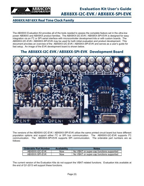
AB08XX/AB18XX Real Time Clock Family<br />
Evaluation Kit User’s <strong>Guide</strong><br />
<strong>ABX8XX</strong>-<strong>I2C</strong>-<strong>EVK</strong> / <strong>ABX8XX</strong>-<strong>SPI</strong>-<strong>EVK</strong><br />
The <strong>ABX8XX</strong> Evaluation Kit provides all of the tools needed to assess the complete feature set in the ultra-low<br />
power AB08XX and <strong>ABX8XX</strong> product families. The <strong>ABX8XX</strong>-<strong>I2C</strong>-<strong>EVK</strong> / <strong>ABX8XX</strong>-<strong>SPI</strong>-<strong>EVK</strong> is designed for easy<br />
integration via an I 2 C or <strong>SPI</strong> serial interface with microcontroller development kits or with custom boards. The<br />
<strong>ABX8XX</strong>-<strong>I2C</strong>-<strong>EVK</strong> / <strong>ABX8XX</strong>-<strong>SPI</strong>-<strong>EVK</strong> may be used for both initial evaluation and product development. This<br />
document provides an overview of the <strong>ABX8XX</strong>-<strong>I2C</strong>-<strong>EVK</strong> / <strong>ABX8XX</strong>-<strong>SPI</strong>-<strong>EVK</strong> and serves as a user’s guide for<br />
fast setup. An image of the <strong>EVK</strong> development board is shown below.<br />
The <strong>ABX8XX</strong>-<strong>I2C</strong>-<strong>EVK</strong> / <strong>ABX8XX</strong>-<strong>SPI</strong>-<strong>EVK</strong> Development Board<br />
The versions of the <strong>ABX8XX</strong>-<strong>I2C</strong>-<strong>EVK</strong> / <strong>ABX8XX</strong>-<strong>SPI</strong>-<strong>EVK</strong> utilize the same printed circuit board but have different<br />
population options and support either I 2 C or <strong>SPI</strong> bus communication. The <strong>ABX8XX</strong>-<strong>I2C</strong>-<strong>EVK</strong> supports I 2 C<br />
communication. The <strong>ABX8XX</strong>-<strong>SPI</strong>-<strong>EVK</strong> supports <strong>SPI</strong> communication. The orderable part numbers are as<br />
follows:<br />
Orderable Part Number Availability Notes<br />
<strong>ABX8XX</strong>-<strong>I2C</strong>-<strong>EVK</strong> Now No VBAT or super-cap functions supported<br />
<strong>ABX8XX</strong>-<strong>SPI</strong>-<strong>EVK</strong> Now No VBAT or super-cap functions supported<br />
The current version of the Evaluation Kits do not support the VBAT-related functions. Evaluation kits available at<br />
the end of Q1-2013 will support these functions.<br />
Page (0)
AB08XX/AB18XX Real Time Clock Family<br />
Evaluation Kit User’s <strong>Guide</strong><br />
<strong>ABX8XX</strong>-<strong>I2C</strong>-<strong>EVK</strong> / <strong>ABX8XX</strong>-<strong>SPI</strong>-<strong>EVK</strong><br />
Table of Contents<br />
The <strong>ABX8XX</strong>-<strong>I2C</strong>-<strong>EVK</strong> / <strong>ABX8XX</strong>-<strong>SPI</strong>-<strong>EVK</strong> Development Board ........................................................................... 0<br />
1. Kit Contents ........................................................................................................................................................ 2<br />
2. <strong>ABX8XX</strong> <strong>EVK</strong> Overview ..................................................................................................................................... 2<br />
3. Component Locations......................................................................................................................................... 4<br />
4. Connector Pin-Outs and Probe Points ............................................................................................................... 7<br />
5. VCC and VBAT Current Measurements with SW1 and SW2 ............................................................................ 9<br />
6. VBAT Backup Power ........................................................................................................................................ 10<br />
7. External 32 kHz Clock ...................................................................................................................................... 10<br />
8. Debug LED ....................................................................................................................................................... 11<br />
9. Installation <strong>Guide</strong> .............................................................................................................................................. 11<br />
9.1 Hardware Setup ................................................................................................................................... 11<br />
9.2 Software Setup .................................................................................................................................... 11<br />
9.3 Measuring Current Draw in the <strong>ABX8XX</strong>-<strong>EVK</strong> .................................................................................... 11<br />
9.4 Measuring Frequency Accuracy in the <strong>ABX8XX</strong>-<strong>EVK</strong> ........................................................................ 13<br />
10. Schematics and Component List ...................................................................................................................... 14<br />
11. Component Installation Differences ................................................................................................................. 21<br />
List of Figures<br />
Figure 1 – <strong>ABX8XX</strong>-<strong>EVK</strong> Block Diagram.................................................................................................................... 3<br />
Figure 2 – <strong>EVK</strong> Board Top Side Components ............................................................................................................ 4<br />
Figure 3 – Top Component Locations ........................................................................................................................ 5<br />
Figure 4 – Bottom Component Locations ................................................................................................................... 6<br />
Figure 5 – 24 Pin Header Connector Pin-out ............................................................................................................. 7<br />
Figure 6 – 5 x 5 Test Point Array Pin-out ................................................................................................................... 9<br />
Figure 7 – VCC and VBAT Current Measurement ................................................................................................... 10<br />
Figure 8 – <strong>ABX8XX</strong>-<strong>I2C</strong>-<strong>EVK</strong> Schematic Page 1 ..................................................................................................... 15<br />
Figure 9 – <strong>ABX8XX</strong>-<strong>I2C</strong>-<strong>EVK</strong> Schematic Page 2 ..................................................................................................... 16<br />
Figure 10 – <strong>ABX8XX</strong>-<strong>SPI</strong>-<strong>EVK</strong> Schematic Page 1 ................................................................................................... 17<br />
Figure 11 – <strong>ABX8XX</strong>-<strong>SPI</strong>-<strong>EVK</strong> Schematic Page 2 ................................................................................................... 18<br />
List of Tables<br />
Table 1 – Top Side Board Component Descriptions .................................................................................................. 4<br />
Table 2 – 24 Pin (2x12) Connector Pin Names and Descriptions .............................................................................. 7<br />
Table 3 – <strong>ABX8XX</strong>-<strong>I2C</strong>-<strong>EVK</strong> Component List .......................................................................................................... 19<br />
Table 4 – <strong>ABX8XX</strong>-<strong>SPI</strong>-<strong>EVK</strong> Component List .......................................................................................................... 20<br />
Table 5 – Component Installation Differences ......................................................................................................... 21<br />
Page (1)
AB08XX/AB18XX Real Time Clock Family<br />
Evaluation Kit User’s <strong>Guide</strong><br />
<strong>ABX8XX</strong>-<strong>I2C</strong>-<strong>EVK</strong> / <strong>ABX8XX</strong>-<strong>SPI</strong>-<strong>EVK</strong><br />
1. Kit Contents<br />
The items included in the <strong>ABX8XX</strong> <strong>EVK</strong> kit are listed below.<br />
• Welcome letter<br />
• One <strong>ABX8XX</strong> <strong>SPI</strong> or <strong>I2C</strong> <strong>EVK</strong> development board.<br />
- <strong>ABX8XX</strong>-<strong>I2C</strong>-<strong>EVK</strong> with I 2 C interface<br />
- <strong>ABX8XX</strong>-<strong>SPI</strong>-<strong>EVK</strong> with <strong>SPI</strong> interface<br />
• <strong>Abracon</strong> USB flash-drive containing the following documentation.<br />
- <strong>ABX8XX</strong> Evaluation Kit User’s <strong>Guide</strong> (this document)<br />
- AB08XX Real Time Clock Family Datasheet<br />
- AB18XX Real Time Clock Family With Power Management Datasheet<br />
- Compiled and tested C code driver functions for the <strong>ABX8XX</strong><br />
- PCB Component Assembly Drawing - Searchable PDF file<br />
- PCB Layout Gerber Files<br />
- PCB Schematics - Searchable PDF file<br />
- <strong>ABX8XX</strong> Power Management Application Note<br />
2. <strong>ABX8XX</strong> <strong>EVK</strong> Overview<br />
The <strong>ABX8XX</strong>-<strong>EVK</strong> should be used with a host microcontroller (e.g., a microcontroller development kit or an<br />
existing production system) to control memory reads and writes over the I 2 C or <strong>SPI</strong> serial interface. All operations<br />
can be initiated over the serial interface including setting time, reading time, setting alarms and timers, clearing<br />
alarms and timers, and other functions described in the datasheet documents “AB08XX Real Time Clock Family”<br />
and “AB18XX Real Time Clock Family with Power Management.” In addition to serial interface access, the <strong>EVK</strong><br />
provides access to all input and output signals on the <strong>ABX8XX</strong>. These signals can be set or read by the host<br />
microcontroller unit (MCU) or any other component in the system. The <strong>ABX8XX</strong> RTC family members support<br />
either the I 2 C or <strong>SPI</strong> serial interface as well as different I/O and power management features. Additional<br />
information about product numbering can be found in the document titled, “<strong>ABX8XX</strong> Part Selection <strong>Guide</strong>.”<br />
The <strong>EVK</strong> also provides test points for making analog measurements. A pico-ammeter can be inserted in series<br />
with the VCC and VBAT supply voltages or between the PCB current measurement test points to measure the<br />
ultra-low current consumption in each of the oscillation modes. Additionally, a high accuracy frequency counter<br />
can be used to measure frequency stability over extended periods under different calibration settings.<br />
Page (2)
AB08XX/AB18XX Real Time Clock Family<br />
Evaluation Kit User’s <strong>Guide</strong><br />
<strong>ABX8XX</strong>-<strong>I2C</strong>-<strong>EVK</strong> / <strong>ABX8XX</strong>-<strong>SPI</strong>-<strong>EVK</strong><br />
Figure 1 shows a block diagram of a typical <strong>EVK</strong> use case.<br />
<strong>EVK</strong> BOARD<br />
VCC<br />
SW1<br />
VBAT<br />
SW2<br />
Super<br />
Capacitor<br />
VCC<br />
<strong>I2C</strong>/<strong>SPI</strong><br />
I/O pin<br />
pull-up<br />
resistors<br />
<strong>I2C</strong>/<strong>SPI</strong> BUS<br />
VCC<br />
<strong>I2C</strong>/<strong>SPI</strong><br />
Ammeter<br />
connection<br />
VBAT<br />
MCU / Host<br />
Controller<br />
VSS<br />
GPIO<br />
GPIO<br />
GPIO<br />
GPIO<br />
GPIO<br />
GPIO<br />
GPIO/RESET<br />
GPIO<br />
nCE/nTIRQ<br />
FOUT/nIRQ<br />
EXTI<br />
AB18XX<br />
AM18XX<br />
CLKOUT/nIRQ3<br />
nEXTR<br />
WDI<br />
nRST<br />
PSW/nIRQ2<br />
VSS<br />
XI<br />
XO<br />
Figure 1 – <strong>ABX8XX</strong>-<strong>EVK</strong> Block Diagram<br />
Access to all <strong>ABX8XX</strong> pins is provided by a 24-pin expansion header connector with 2mm x 2mm pin spacing.<br />
The <strong>EVK</strong> board also comes with 2-pin VCC and VBAT current measurement pins as shown in Figure 2.<br />
Page (3)
AB08XX/AB18XX Real Time Clock Family<br />
Evaluation Kit User’s <strong>Guide</strong><br />
<strong>ABX8XX</strong>-<strong>I2C</strong>-<strong>EVK</strong> / <strong>ABX8XX</strong>-<strong>SPI</strong>-<strong>EVK</strong><br />
3. Component Locations<br />
This section describes key <strong>EVK</strong> board components and their locations on the top and bottom sides of the board.<br />
The top side <strong>EVK</strong> components are labeled in Figure 2 and are described in Table 1.<br />
Figure 2 – <strong>EVK</strong> Board Top Side Components<br />
Board Component<br />
24-pin header connector<br />
Super capacitor<br />
VCC current measurement pins<br />
VBAT current measurement pins<br />
Table 1 – Top Side Board Component Descriptions<br />
Description<br />
This is the top side of the 24 pin connector used to make power and<br />
input/output pin signal connections to the <strong>EVK</strong> board. This is a 2x12,<br />
2mm pitch connector (see <strong>EVK</strong> component list for part number). The<br />
connector can be used to connect to individual pin headers, ribbon cable<br />
connectors, or can be used as a module and plug into a female connector<br />
on the host target system.<br />
Can be used as the VBAT (backup) supply power source of the <strong>ABX8XX</strong>.<br />
These pins are in series with the VCC supply pin of the <strong>ABX8XX</strong> and are<br />
used to connect to an external pico-ammeter for measuring the VCC<br />
current into the <strong>ABX8XX</strong> device. The connection polarity is shown in the<br />
diagram.<br />
These pins are in series with the VBAT supply pin of the <strong>ABX8XX</strong> and are<br />
used to connect to an external pico-ammeter for measuring the VBAT<br />
current into the <strong>ABX8XX</strong> device. The connection polarity is shown in the<br />
diagram.<br />
Page (4)
AB08XX/AB18XX Real Time Clock Family<br />
Evaluation Kit User’s <strong>Guide</strong><br />
<strong>ABX8XX</strong>-<strong>I2C</strong>-<strong>EVK</strong> / <strong>ABX8XX</strong>-<strong>SPI</strong>-<strong>EVK</strong><br />
Board Component<br />
LED<br />
SW1<br />
SW2<br />
32.768kHz crystal<br />
AB180X / AB181X<br />
MMCX Footprint<br />
Description<br />
A separate pin on the 24-pin socket connector connects to the LED. This<br />
LED can be controlled by an MCU GPIO pin or can be connected directly<br />
to the VCC or VBAT supply to indicate one of the supplies has power<br />
applied.<br />
This switch is connected in parallel with the VCC current measurement<br />
pins. It is used to short across the pins and connect the external VCC<br />
supply to the <strong>ABX8XX</strong> when not measuring current with the picoammeter.<br />
This switch is connected in parallel with the VBAT current measurement<br />
pins. It is used to short across the pins and connect the external VBAT<br />
supply to the <strong>ABX8XX</strong> when not measuring current with the picoammeter.<br />
The crystal is connected to the XI and XO pins of the <strong>ABX8XX</strong> device<br />
I 2 C (AB180X) or <strong>SPI</strong> (AB181X) real time clock device.<br />
This can be used for providing an external clock input.<br />
The top and bottom component locations and their corresponding reference designators are shown in Figure 3<br />
and Figure 4. A searchable PDF file of the top and bottom board assembly drawings with reference designators<br />
is also included in the USB flash drive documentation to allow for quick location of components in the board<br />
schematics.<br />
Figure 3 – Top Component Locations<br />
Page (5)
AB08XX/AB18XX Real Time Clock Family<br />
Evaluation Kit User’s <strong>Guide</strong><br />
<strong>ABX8XX</strong>-<strong>I2C</strong>-<strong>EVK</strong> / <strong>ABX8XX</strong>-<strong>SPI</strong>-<strong>EVK</strong><br />
Figure 4 – Bottom Component Locations<br />
Page (6)
AB08XX/AB18XX Real Time Clock Family<br />
Evaluation Kit User’s <strong>Guide</strong><br />
<strong>ABX8XX</strong>-<strong>I2C</strong>-<strong>EVK</strong> / <strong>ABX8XX</strong>-<strong>SPI</strong>-<strong>EVK</strong><br />
4. Connector Pin-Outs and Probe Points<br />
Figure 5 shows the location of the names and numbers each of the pins (pin-out) of the 24-pin header connector.<br />
nEXTR<br />
WDI<br />
GND<br />
EXTI<br />
<strong>SPI</strong>_nCE<br />
<strong>SPI</strong>_MISO<br />
GND<br />
<strong>I2C</strong>_SCL<br />
VCC_AM_IMSR<br />
VBAT_AM_IMSR<br />
VTEMP<br />
VPP_CONN<br />
1 2<br />
3 4<br />
5 6<br />
7 8<br />
9 10<br />
11 12<br />
13 14<br />
15 16<br />
17 18<br />
19 20<br />
21 22<br />
23 24<br />
nRST<br />
CLKOUT<br />
FOUT<br />
PSW<br />
<strong>SPI</strong>_MOSI<br />
<strong>SPI</strong>_SCK<br />
VCC_IO<br />
<strong>I2C</strong>_SDA<br />
GND<br />
SUCAP_DIS<br />
LED<br />
VSYS<br />
Figure 5 – 24 Pin Header Connector Pin-out<br />
Table 2 lists the numbers, names, and descriptions for each pin of the 24-pin (2x12) connector. There are also<br />
pull-up resistors on the board from the pin to the VCC_IO supply. Pull-up values are indicated in the table.<br />
Table 2 – 24 Pin (2x12) Connector Pin Names and Descriptions<br />
Page (7)
AB08XX/AB18XX Real Time Clock Family<br />
Evaluation Kit User’s <strong>Guide</strong><br />
<strong>ABX8XX</strong>-<strong>I2C</strong>-<strong>EVK</strong> / <strong>ABX8XX</strong>-<strong>SPI</strong>-<strong>EVK</strong><br />
Pin<br />
Number<br />
Pin Name<br />
Board<br />
Pull-up<br />
Resistor<br />
Description<br />
1 nEXTR 10k<br />
Connection to the external interrupt input pin (nEXTR) of the<br />
<strong>ABX8XX</strong>.<br />
2 nRST 10k Connection to the external reset output pin (nRST) of the <strong>ABX8XX</strong>.<br />
3 WDI 10k<br />
Connection to the watchdog timer reset input pin (WDI) of the<br />
<strong>ABX8XX</strong>.<br />
4 CLKOUT --<br />
Connection to the square wave output pin (CLKOUT) of the<br />
<strong>ABX8XX</strong>.<br />
5 GND -- PCB GND connection. There is a single GND plane net for the PCB.<br />
Connection to the primary interrupt output pin (FOUT/nIRQ) of the<br />
6 FOUT 10k <strong>ABX8XX</strong>. This pin can also be used to drive the <strong>ABX8XX</strong> square<br />
wave output.<br />
7 EXTI 10k Connection to the external interrupt input pin (EXTI) of the <strong>ABX8XX</strong>.<br />
Connection secondary interrupt output pin (PSW/nIRQ2) of the<br />
8 PSW 10k <strong>ABX8XX</strong>. It can also drive the square wave output or function as the<br />
power switch to power gate external devices.<br />
<strong>ABX8XX</strong>-<strong>I2C</strong>-<strong>EVK</strong> board: Connection to the timer output pin<br />
9 <strong>SPI</strong>_nCE / nTIRQ 10k<br />
(nTIRQ) of the <strong>ABX8XX</strong>.<br />
<strong>ABX8XX</strong>-<strong>SPI</strong>-<strong>EVK</strong> board: Connection to the I/O interface <strong>SPI</strong> chip<br />
select input pin (nCE) of the <strong>ABX8XX</strong>.<br />
<strong>ABX8XX</strong>-<strong>I2C</strong>-<strong>EVK</strong> board: Not connected.<br />
10 <strong>SPI</strong>_MOSI --<br />
<strong>ABX8XX</strong>-<strong>SPI</strong>-<strong>EVK</strong> board: <strong>SPI</strong> master out / slave in data signal.<br />
Connects to the I/O interface <strong>SPI</strong> data input pin (SDI) of the<br />
<strong>ABX8XX</strong>.<br />
<strong>ABX8XX</strong>-<strong>I2C</strong>-<strong>EVK</strong> board: Not connected.<br />
11 <strong>SPI</strong>_MISO --<br />
<strong>ABX8XX</strong>-<strong>SPI</strong>-<strong>EVK</strong> board: <strong>SPI</strong> master in / slave out data signal.<br />
Connects to the I/O interface <strong>SPI</strong> data output pin (SD0) of the<br />
<strong>ABX8XX</strong>.<br />
<strong>ABX8XX</strong>-<strong>I2C</strong>-<strong>EVK</strong> board: Not connected.<br />
12 <strong>SPI</strong>_SCK --<br />
<strong>ABX8XX</strong>-<strong>SPI</strong>-<strong>EVK</strong> board: Connects to the I/O interface clock pin<br />
(SCL) of the <strong>ABX8XX</strong>. It provides the clock input for <strong>SPI</strong> interface<br />
mode.<br />
13 GND -- PCB GND connection. There is a single GND plane net for the PCB.<br />
This supply connection pin provides power to the board pull-up<br />
14 VCC_IO --<br />
resistors and temperature sensor IC. The VCC_AM_IMSR and<br />
VCC_IO connector pins should be connected to the same voltage<br />
level.<br />
<strong>ABX8XX</strong>-<strong>I2C</strong>-<strong>EVK</strong> board: Connects to the I/O interface clock pin<br />
15 <strong>I2C</strong>_SCL 2.2k<br />
(SCL) of the <strong>ABX8XX</strong>. It provides the clock input for I 2 C interface<br />
mode.<br />
<strong>ABX8XX</strong>-<strong>SPI</strong>-<strong>EVK</strong> board: Not connected.<br />
<strong>ABX8XX</strong>-<strong>I2C</strong>-<strong>EVK</strong> board: Connects to the I 2 C interface data I/O pin<br />
16 <strong>I2C</strong>_SDA 2.2k (SDA) of the <strong>ABX8XX</strong>.<br />
<strong>ABX8XX</strong>-<strong>SPI</strong>-<strong>EVK</strong> board: Not connected.<br />
This supply connection pin provides power to VCC supply pin of the<br />
17 VCC_AM_IMSR -- <strong>ABX8XX</strong> through SW1. The VCC_AM_IMSR and VCC_IO<br />
connector pins should be connected to the same voltage level.<br />
18 GND -- PCB GND connection. There is a single GND plane net for the PCB.<br />
This supply connection pin provides power to VBAT supply pin of the<br />
19 VBAT_AM_IMSR -- <strong>ABX8XX</strong> through SW2. It can be used to provide the backup power<br />
source to the <strong>ABX8XX</strong>.<br />
Page (8)
AB08XX/AB18XX Real Time Clock Family<br />
Evaluation Kit User’s <strong>Guide</strong><br />
<strong>ABX8XX</strong>-<strong>I2C</strong>-<strong>EVK</strong> / <strong>ABX8XX</strong>-<strong>SPI</strong>-<strong>EVK</strong><br />
Pin<br />
Number<br />
Pin Name<br />
Board<br />
Pull-up<br />
Resistor<br />
20 SUCAP_DIS --<br />
21 VTEMP --<br />
22 LED --<br />
23 VSYS -- Test point<br />
24 VPP_CON -- Test point<br />
Description<br />
Super capacitor disconnect signal. This signal can be used to<br />
connect/disconnect the super capacitor from the <strong>ABX8XX</strong> VBAT pin.<br />
Additional component population changes are required to use this<br />
feature.<br />
This is the analog voltage output from the temperature sensor IC on<br />
the board. The temperature sensor IC is not populated on the board<br />
by default.<br />
This pin connects to the debug LED populated on the board through<br />
a 510 ohm resistor.<br />
A 5 x 5 array of probe points for the <strong>ABX8XX</strong> device is provided on the <strong>EVK</strong> board around the perimeter of the<br />
device package as shown in Figure 6. This enables users to probe or connect wires to the pins of the <strong>ABX8XX</strong><br />
device for test and debug.<br />
Figure 6 – 5 x 5 Test Point Array Pin-out<br />
5. VCC and VBAT Current Measurements with SW1 and SW2<br />
The <strong>ABX8XX</strong> VCC and VBAT supply current can be measured by connecting an ammeter to the VCC and VBAT<br />
current measurement pins. The VCC and VBAT current measurement pins and +/- polarity are shown in Figure 2.<br />
SW1 is connected across the + and – terminals of the VCC current measurement pins and SW2 is connected<br />
across the + and – terminals of the VBAT current measurement pins.<br />
Page (9)
AB08XX/AB18XX Real Time Clock Family<br />
Evaluation Kit User’s <strong>Guide</strong><br />
<strong>ABX8XX</strong>-<strong>I2C</strong>-<strong>EVK</strong> / <strong>ABX8XX</strong>-<strong>SPI</strong>-<strong>EVK</strong><br />
SW1 and SW2 are placed in the “open” position by sliding the switch lever to the left side as shown in Figure 7.<br />
They are placed in the “closed” position by sliding the switch lever to the right side.<br />
When the switch is placed in the “open” position, the VCC/VBAT connection to the <strong>ABX8XX</strong> device becomes an<br />
open circuit. This forces current to flow through the VCC/VBAT current measurements pins and enables current<br />
measurement with an ammeter. When the switch is placed in the “closed” position, a short circuit is placed<br />
across the terminals of the VCC/VBAT current measurement pins. If an ammeter is still connected, its terminals<br />
will also get shorted together. This allows the ammeter to be removed from the VCC/VBAT current measurement<br />
pins without losing power to the <strong>ABX8XX</strong> device. If an ammeter is not connected to the VCC/VBAT current<br />
measurement pins, the switch should be placed in the “closed” position to supply power to the <strong>ABX8XX</strong> device<br />
from the 24-pin connector.<br />
Figure 7 – VCC and VBAT Current Measurement<br />
6. VBAT Backup Power<br />
Backup power to the <strong>ABX8XX</strong> VBAT pin can be provided using the 24-pin connector or the on-board super<br />
capacitor. The super capacitor can be connected to the VBAT pin of the <strong>ABX8XX</strong> by populating 0 ohm resistors<br />
or solder shorts across R10 and R16. This will allow continued time keeping, register/memory state retention, etc.<br />
should the VCC supply be removed. Information about using the <strong>ABX8XX</strong> integrated trickle charger to charge the<br />
super capacitor can be found in the datasheet document “<strong>ABX8XX</strong> Real Time Clock Family with Power<br />
Management.”<br />
7. External 32 kHz Clock<br />
An external 32.768 kHz clock can be supplied to the <strong>ABX8XX</strong> device via the MMCX connector footprint shown in<br />
Figure 2. The middle pin of this connector footprint connects to the XO pin of the <strong>ABX8XX</strong> device. An MMCX<br />
connector (part number provide in the component list of Table 3 and Table 4) or other can be soldered to these<br />
pins to connect to an external frequency generator. The external clock must not exceed either the VCC supply or<br />
1.8V (maximum input voltage), whichever is less.<br />
Page (10)
AB08XX/AB18XX Real Time Clock Family<br />
Evaluation Kit User’s <strong>Guide</strong><br />
<strong>ABX8XX</strong>-<strong>I2C</strong>-<strong>EVK</strong> / <strong>ABX8XX</strong>-<strong>SPI</strong>-<strong>EVK</strong><br />
To connect the MMCX connector to the XO pin of the <strong>ABX8XX</strong> device, remove the crystal from the board and<br />
populate R28 with a 0 ohm resistor or solder short.<br />
8. Debug LED<br />
A debug/indicator LED is provided on the board and has an individual pin connection to the 24 pin connector.<br />
There is a 510 ohm resistor in series with the LED with the cathode of the LED connected to GND. The LED can<br />
be connected directly to the VCC_IO supply to indicate when power is supplied to the board or it can be<br />
connected to an MCU GPIO pin.<br />
9. Installation <strong>Guide</strong><br />
This section provides a guide for setting up the <strong>EVK</strong> to quickly evaluate the AB08XX and <strong>ABX8XX</strong> product<br />
families. It is assumed in the subsequent discussion that a microcontroller development kit is being used as a<br />
Host Controller (HC). It is also assumed that the HC has accessible pins for I 2 C or <strong>SPI</strong> communication and<br />
accessible GPIO pins for interfacing with the other <strong>ABX8XX</strong>-<strong>EVK</strong> pins.<br />
9.1 Hardware Setup<br />
1. Begin with the <strong>ABX8XX</strong>-<strong>EVK</strong> and HC development boards powered down.<br />
2. For the <strong>ABX8XX</strong>-<strong>I2C</strong>-<strong>EVK</strong>, connect the <strong>I2C</strong>_SDA (pin 16) and <strong>I2C</strong>_SCL (pin 15) pins on the <strong>EVK</strong> 24 pin<br />
connector to the SDA and SCL pins on the HC development board. For the <strong>ABX8XX</strong>-<strong>SPI</strong>-<strong>EVK</strong>, connect<br />
the <strong>SPI</strong>_SCK (pin 12), <strong>SPI</strong>_MISO (pin 11), <strong>SPI</strong>_MOSI (pin 10) and <strong>SPI</strong>_nCE/nTIRQ (pin 9) pins on the<br />
<strong>EVK</strong> connector to the corresponding pins on the HC development board.<br />
3. Connect any other digital inputs/outputs of interest on the <strong>ABX8XX</strong>-<strong>EVK</strong> development board connector to<br />
GPIO pins on the HC.<br />
4. Connect the VCC, VBAT (if applicable), and VSS pins on the <strong>EVK</strong> connector to appropriate supply<br />
voltages. The VCC supply voltage should be connected to both VCC_AM_IMSR (pin 17) and VCC_IO<br />
(pin 14) (see Figure 5). The VBAT supply voltage should be connected to VCC_AM_IMSR (pin 19). The<br />
HC VCC and <strong>ABX8XX</strong> VCC supplies should be the same voltage.<br />
5. Power up the <strong>ABX8XX</strong>-<strong>EVK</strong> and HC development boards.<br />
9.2 Software Setup<br />
The <strong>ABX8XX</strong>-<strong>EVK</strong> does not require any host PC software installation but does require minimal driver<br />
development for the HC. All drivers are simple sequences of I 2 C or <strong>SPI</strong> register writes. Detailed information on<br />
each register in the <strong>ABX8XX</strong> products can be found in the datasheet documents titled, “AB08XX Real Time Clock<br />
Family” and “<strong>ABX8XX</strong> Real Time Clock Family with Power Management.”<br />
9.3 Measuring Current Draw in the <strong>ABX8XX</strong>-<strong>EVK</strong><br />
To measure current draw on the <strong>ABX8XX</strong>-<strong>EVK</strong>, an ammeter must be inserted in series with the <strong>ABX8XX</strong> part,<br />
and the part must then be put into a desired oscillation state. Listed below are the steps required to measure<br />
current through the <strong>ABX8XX</strong> VCC pin in the most energy-efficient setting in crystal (XT) oscillation and RC<br />
oscillation modes.<br />
1. Complete Steps 1-4 in Section 9.1.<br />
2. Connect an ammeter in series with the VCC pin on the <strong>ABX8XX</strong> part. This is done most easily by first<br />
connecting an ammeter between the VCC current measurement pins (see Figure 7). Power on the<br />
ammeter and set it to a range setting capable of measuring mA or tens of mA. To measure positive<br />
current, the ammeter polarity should be connected following the VCC Current Measurement polarity<br />
Page (11)
AB08XX/AB18XX Real Time Clock Family<br />
Evaluation Kit User’s <strong>Guide</strong><br />
<strong>ABX8XX</strong>-<strong>I2C</strong>-<strong>EVK</strong> / <strong>ABX8XX</strong>-<strong>SPI</strong>-<strong>EVK</strong><br />
markers (+/-) shown in Figure 2. Once the ammeter is connected, change the position of SW1 to the<br />
open position (see Figure 7).<br />
3. Power up the <strong>ABX8XX</strong>-<strong>EVK</strong> and HC development boards.<br />
4. Issue a series of commands to place the <strong>ABX8XX</strong> part in a typical low current oscillation state. The<br />
examples here use the I/O access functions readreg and writereg described in the pseudo code<br />
a. Set the OUT bit (register 0x10 bit 4) to 1 and the OUT1S field (register 0x11 bits [1:0]) to 0 to<br />
insure the OUT1 pin is high and not drawing current through the pullup resistor. Set the OUTB bit<br />
(register 0x10 bit 5) to 1 and the OUT2S field (register 0x11 bits [4:2]) to 0 to insure the OUT2 pin<br />
is high and not drawing current through the pullup resistor. Set the RS1E bit (register 0x11 bit 5)<br />
to 0 to disable the external reset input. This should force the nRST pin to be high and not draw<br />
current through the pullup resistor.<br />
temp = readreg(0x10) // Read the Control1 Register<br />
writereg(0x10, temp | 0x30) // Set the OUT and OUTB bits<br />
temp = readreg(0x11) // Read the Control2 Register<br />
writereg(0x11, temp & 0xC0) // Set the OUT1S, OUT2S and RS1E fields to 0<br />
b. Set the IM field (register 0x12 bits [6:5]) to 0x3. This will minimize the current drawn by the alarm<br />
interrupt pulse generator.<br />
temp = readreg(0x12)<br />
writereg(0x10, temp | 0x60)<br />
// Read the Interrupt Mask Register<br />
// Set the IM field to 0x3<br />
c. Set the TE bit low and the TFS field to 0x3 by writing the value 0x03 to register 0x18. This will<br />
minimize internal current drawn by the Countdown Timer and insure the OUT3 pin is high and not<br />
drawing current through the pullup resistor.<br />
writereg(0x13, 0x03)<br />
// Set the TE bit to 0 and the TFS field to 0x3<br />
d. Set the SQWE bit (register 0x13 bit 7) to 0 to disable the output square wave generator and<br />
insure that the OUT4 pin is not toggling.<br />
temp = readreg(0x13) // Read the SQW Register<br />
writereg(0x13, temp & 0x7F) // Set the SQWE bit to 0<br />
e. To observe the current with the Crystal oscillator running, set the OSEL bit (register 0x1C bit 7) to<br />
0. Note that register 0x1F MUST be written with the value 0xA1 prior to any attempt to modify<br />
register 0x1C.<br />
temp = readreg(0x1C) // Read the Oscillator Control Register<br />
writereg(0x1F, 0xA1)<br />
// Load the Configuration Key Register with 0xA1<br />
writereg(0x1C, temp & 0x7F) // Set the OSEL bit to 0<br />
f. To observe the current with the RC oscillator running, set the OSEL bit (register 0x1C bit 7) to 1.<br />
Note that register 0x1F MUST be written with the value 0xA1 prior to any attempt to modify<br />
register 0x1C.<br />
temp = readreg(0x1C) // Read the Oscillator Control Register<br />
writereg(0x1F, 0xA1)<br />
// Load the Configuration Key Register with 0xA1<br />
writereg(0x1C, temp | 0x80) // Set the OSEL bit to 1<br />
Page (12)
AB08XX/AB18XX Real Time Clock Family<br />
Evaluation Kit User’s <strong>Guide</strong><br />
<strong>ABX8XX</strong>-<strong>I2C</strong>-<strong>EVK</strong> / <strong>ABX8XX</strong>-<strong>SPI</strong>-<strong>EVK</strong><br />
g. The calendar counter registers (registers 0x0 through 0x7) may be read to verify that the internal<br />
timing system is operational.<br />
5. Change the ammeter range to a setting capable of measuring nA and observe the current draw.<br />
Averaging and filtering functions can help eliminate minor fluctuations in current caused by environmental<br />
radiation.<br />
Note that nA current measurements can be influenced by both environmental conditions and equipment selection.<br />
Contact <strong>Abracon</strong> support at tech-support@abracon.com with any questions about measurement conditions.<br />
9.4 Measuring Frequency Accuracy in the <strong>ABX8XX</strong>-<strong>EVK</strong><br />
To measure frequency accuracy on the <strong>ABX8XX</strong>-<strong>EVK</strong>, a high-precision universal counter should be used to<br />
monitor the frequency output on the CLKOUT pin. Follow the steps below to achieve a high accuracy reading in<br />
crystal (XT) oscillation mode, RC oscillation mode, or autocalibration mode.<br />
1. Complete Steps 1-4 in Section 9.1.<br />
2. Connect a universal counter to Pin 4 of the 24-pin expansion connector in Figure 5. Choose a long<br />
integration time on the universal counter (e.g., 10 seconds) to ensure that a sufficient number of clock<br />
periods are captured.<br />
3. Power up the <strong>ABX8XX</strong>-<strong>EVK</strong> and HC development boards.<br />
4. Place the <strong>ABX8XX</strong> part in a typical oscillation state by setting the SQWE bit (register 0x13 bit 7) to 1, and<br />
the SQFS field (register 0x13 bits [4:0]) to select a low frequency used to measure the internal oscillation<br />
modes. A frequency of 1 Hz (SQFS = 0xF) allows easy interpretation of the frequency error.<br />
writereg(0x13, 0x8F)<br />
// Set the SQWE bit to 1 and the SQFS field to 0xF<br />
5. Note that if the <strong>ABX8XX</strong> is driving an external clock signal, the current drawn will be significantly higher<br />
than the current observed in low power mode.<br />
6. Observe the frequency reported by the universal counter. For short integration times, the frequency may<br />
appear to fluctuate for the RC oscillator, in particular. This is a result of calibration and does not affect<br />
long term accuracy. Record frequency measurements over extended periods of hours or days to achieve<br />
the most accurate data.<br />
a. To observe the Crystal oscillator, set the OSEL bit (register 0x1C bit 7) to 0. Note that register<br />
0x1F MUST be written with the value 0xA1 prior to any attempt to modify register 0x1C.<br />
temp = readreg(0x1C) // Read the Oscillator Control Register<br />
writereg(0x1F, 0xA1)<br />
// Load the Configuration Key Register with 0xA1<br />
writereg(0x1C, temp & 0x7F) // Set the OSEL bit to 0<br />
b. To observe the RC oscillator, set the OSEL bit (register 0x1C bit 7) to 1. Note that register 0x1F<br />
MUST be written with the value 0xA1 prior to any attempt to modify register 0x1C.<br />
temp = readreg(0x1C) // Read the Oscillator Control Register<br />
writereg(0x1F, 0xA1)<br />
// Load the Configuration Key Register with 0xA1<br />
writereg(0x1C, temp | 0x80) // Set the OSEL bit to 1<br />
c. To observe the RC oscillator while autocalibration is active, set the OSEL bit (register 0x1C bit 7)<br />
to 1 and the ACAL field (register 1C bits [6:5]) to 0x3. Note that register 0x1F MUST be written<br />
with the value 0xA1 prior to any attempt to modify register 0x1C. This will enable autocalibration<br />
of the RC oscillator to occur every 512 seconds (roughly every 8.5 minutes). The first<br />
autocalibration cycle will begin as soon as ACAL is set to 0x3, and will be completed with a new<br />
RC calibration value in the CALRC registers (registers 0x15 and 0x16) within 60 seconds.<br />
Page (13)
AB08XX/AB18XX Real Time Clock Family<br />
Evaluation Kit User’s <strong>Guide</strong><br />
<strong>ABX8XX</strong>-<strong>I2C</strong>-<strong>EVK</strong> / <strong>ABX8XX</strong>-<strong>SPI</strong>-<strong>EVK</strong><br />
temp = readreg(0x1C)<br />
temp = temp & 0x9F<br />
writereg(0x1C, temp | 0x60)<br />
// Read the Oscillator Control Register<br />
// Mask the ACAL field<br />
// Set the OSEL bit to 1 and the ACAL field to 0x2<br />
Note that frequency accuracy measurements are heavily influenced by test equipment. Contact <strong>Abracon</strong> support<br />
at tech-support@abracon.com with any questions about proper test setup.<br />
10. Schematics and Component List<br />
Figure 8 and Figure 9 below show the two pages of the <strong>ABX8XX</strong>-<strong>I2C</strong>-<strong>EVK</strong> board schematics. Figure 10 and<br />
Figure 11 show the two pages of the <strong>ABX8XX</strong>-<strong>SPI</strong>-<strong>EVK</strong> board schematics. Table 3 shows the <strong>ABX8XX</strong>-<strong>I2C</strong>-<strong>EVK</strong><br />
board component list and Table 4 shows the <strong>ABX8XX</strong>-<strong>SPI</strong>-<strong>EVK</strong> board component list. Board components labeled<br />
as DNP (do not populate) in the schematics are not installed on the board.<br />
Page (14)
AB08XX/AB18XX Real Time Clock Family<br />
Evaluation Kit User’s <strong>Guide</strong><br />
<strong>ABX8XX</strong>-<strong>I2C</strong>-<strong>EVK</strong> / <strong>ABX8XX</strong>-<strong>SPI</strong>-<strong>EVK</strong><br />
AM18XX16 PIN 3x3MM QFN<br />
AB18XX PIN 3x3mm QFN<br />
XO<br />
Y1<br />
32.768 kHz<br />
DNP<br />
XI<br />
1 2<br />
GND<br />
Y2<br />
32.768 kHz<br />
C2<br />
1.0pF<br />
DNP<br />
nRST<br />
WDI<br />
nEXTR<br />
PSW<br />
1 2<br />
VCC_IO<br />
VCC_IO<br />
Y 3<br />
32.768 kHz<br />
DNP<br />
R8<br />
10.0k<br />
R11<br />
10.0k<br />
1 2<br />
U3<br />
AM18x5<br />
C1<br />
1.0pF<br />
DNP<br />
R3<br />
0 ohm<br />
DNP<br />
1<br />
2 nRST<br />
3 WDI<br />
4 nEXTR<br />
PSW/nIRQ2<br />
XI 16<br />
XO 15<br />
14<br />
VSS/VPP<br />
13<br />
VCC 13<br />
VBAT<br />
SDA/SDO<br />
SCL<br />
CLKOUT/nIRQ3<br />
GND<br />
VPP<br />
VCC_AM<br />
12<br />
nTIRQ/nCE<br />
FOUT/nIRQ 11<br />
10<br />
EXTI 9<br />
VSS/SDI<br />
R4<br />
0 ohm<br />
VCC_IO<br />
R5<br />
10.0k<br />
VPP_CON<br />
R12<br />
0 ohm<br />
R6<br />
10.0k<br />
nCE<br />
FOUT<br />
EXTI<br />
SDI<br />
VSYS<br />
AM18XX Test Points<br />
AB18XX Test Points<br />
R7<br />
0 ohm<br />
DNP<br />
nRST<br />
WDI<br />
nEXTR<br />
PSW<br />
XO<br />
XI<br />
U2<br />
AM18x5_20pin<br />
DNP<br />
VBAT_AM<br />
VPP<br />
XI<br />
20<br />
XO 19<br />
1<br />
2 nRST<br />
3 WDI<br />
4 VSY S1<br />
5 nRST1/nEXTR<br />
OUT2/PSW/nIRQ2<br />
VCC_AM<br />
VPP 18<br />
VCC 17<br />
nTIRQ/nCE 16<br />
15<br />
FOUT/nIRQ/OUT1 14<br />
EXTI 13<br />
VSS/SDI 12<br />
VSYS2 11<br />
CLKOUT/nIRQ3/OUT4<br />
VBAT<br />
VSS<br />
ISEL<br />
SDO/SDA<br />
SCL<br />
10<br />
6<br />
7<br />
8<br />
9<br />
nCE<br />
VSS_PAD 21<br />
VCC_AM<br />
GND<br />
FOUT<br />
EXTI<br />
SDI<br />
CLKOUT<br />
VCC_IO<br />
R33<br />
10.0k<br />
R34<br />
10.0k<br />
R35<br />
10.0k<br />
WDI<br />
nEXTR<br />
EXTI<br />
VBAT_AM<br />
5<br />
6<br />
7<br />
8<br />
VCC_IO<br />
R20<br />
2.2k<br />
R21<br />
2.2k<br />
VSS_PAD 17 CLKOUT<br />
GND<br />
R22<br />
10.0k<br />
DNP<br />
SCL<br />
SDA<br />
GND<br />
SCL<br />
SDA<br />
GND<br />
R17<br />
47k<br />
DNP<br />
R23<br />
47k<br />
DNP<br />
<strong>SPI</strong>/<strong>I2C</strong><br />
INTERFACE<br />
SELECT<br />
R19<br />
0 ohm<br />
DNP<br />
ISEL<br />
SUPERCAP DISCONNECT CIRCUIT<br />
This circuit allows the super capacitor to be disconnected from<br />
the VBAT pin using the SUCAP_DIS signal. A logic high voltage<br />
(at or above both the supercap and VBAT_AM_IMSR voltage<br />
levels) will disconnect the super cap from the VBAT_AM_IMSR<br />
net. A logic low voltage (0V) will connect the super cap to the<br />
VBAT_AM_IMSR net. Populate R10 and R16 to bypass.<br />
VBAT_AM_IMSR<br />
AB18XX AMX80X 88 PIN Pin SOIC<br />
VBAT_AM<br />
PSW<br />
R1<br />
0 ohm<br />
DNP<br />
R2<br />
0 ohm<br />
DNP<br />
XI<br />
XO<br />
GND<br />
U1<br />
AMx80x_SOIC<br />
DNP<br />
1<br />
2 XI<br />
3 X0<br />
4 PSW/nIRQ2/VBAT<br />
VSS<br />
VCC 8<br />
FOUT/nIRQ 7<br />
SCL 6<br />
SDA 5<br />
VCC_AM<br />
SUCAP_DIS<br />
R13<br />
51 ohm<br />
DNP<br />
D1<br />
ESD5V3S1U-02LRH<br />
DNP<br />
EXTERNAL CLOCK INPUT<br />
GND<br />
R18<br />
10.0k<br />
DNP<br />
+ C4<br />
30mF<br />
SUPERCAP<br />
GND<br />
2<br />
5<br />
LED<br />
6<br />
3<br />
R10<br />
0 ohm<br />
1<br />
4<br />
Q1<br />
Si1023X<br />
DNP<br />
R16<br />
0 ohm<br />
DNP<br />
INTERFACE SELECTION<br />
nCE<br />
SDI<br />
SCL<br />
SDA<br />
R9<br />
0 ohm<br />
DNP<br />
R14<br />
0 ohm<br />
DNP<br />
R15<br />
0 ohm<br />
R24<br />
0 ohm<br />
DNP<br />
R25<br />
0 ohm<br />
<strong>SPI</strong>_nCE<br />
<strong>SPI</strong>_MOSI<br />
<strong>SPI</strong>_SCK<br />
<strong>I2C</strong>_SCL<br />
<strong>SPI</strong>_MISO<br />
<strong>I2C</strong>_SDA<br />
Option to connect VCC_IO<br />
to VCC_AM_IMSR<br />
R30<br />
VCC_IO 0 ohm VCC_AM_IMSR<br />
DNP<br />
TEMPERATURE MEASUREMENT<br />
VCC_IO<br />
C11<br />
0.1uF<br />
DNP<br />
GND<br />
U4<br />
TMP20AIDRL<br />
DNP<br />
4<br />
3<br />
5 V+ VOUT 2<br />
6 NC2GND 1<br />
GNDNC1<br />
GND<br />
VTEMP<br />
XO<br />
R28<br />
0 ohm<br />
DNP<br />
1<br />
J29<br />
MMCX-J-P-X-RA-TH1<br />
DNP<br />
2<br />
R27<br />
510 ohm<br />
D2<br />
LED_GREEN<br />
1<br />
2<br />
3<br />
4<br />
5<br />
FOUT<br />
SCL<br />
SDA<br />
+ C6<br />
15mF<br />
SUPERCAP<br />
DNP<br />
GND<br />
GND<br />
Figure 8 – <strong>ABX8XX</strong>-<strong>I2C</strong>-<strong>EVK</strong> Schematic Page 1<br />
Page (15)
AB08XX/AB18XX Real Time Clock Family<br />
Evaluation Kit User’s <strong>Guide</strong><br />
<strong>ABX8XX</strong>-<strong>I2C</strong>-<strong>EVK</strong> / <strong>ABX8XX</strong>-<strong>SPI</strong>-<strong>EVK</strong><br />
VCC_AM_IMSR<br />
VCC_AM_IMSR<br />
VCC_IO<br />
VCC_IO<br />
MAIN BOARD TO DAUGHTERCARD CONNECTORS<br />
VPP_CON<br />
CLKOUT<br />
nRST<br />
WDI<br />
nEXTR<br />
PSW<br />
<strong>I2C</strong>_SCL<br />
<strong>SPI</strong>_SCK<br />
VTEMP<br />
CLKOUT<br />
nRST<br />
WDI<br />
nEXTR<br />
PSW<br />
<strong>I2C</strong>_SCL<br />
<strong>SPI</strong>_SCK<br />
40 PIN CONNECTOR<br />
GND<br />
20 PIN CONNECTOR<br />
For smaller daughter cards<br />
J31<br />
HDR_2x10<br />
DNP<br />
2 1<br />
4 3<br />
6 5<br />
8 7<br />
10 9<br />
12<br />
14<br />
16<br />
18<br />
20<br />
2<br />
4<br />
6<br />
8<br />
10<br />
12<br />
14<br />
16<br />
18<br />
20<br />
22<br />
24<br />
26<br />
28<br />
30<br />
32<br />
34<br />
36<br />
38<br />
40<br />
11<br />
13<br />
15<br />
17<br />
19<br />
1<br />
3<br />
5<br />
7<br />
9<br />
11<br />
13<br />
15<br />
17<br />
19<br />
21<br />
23<br />
25<br />
27<br />
29<br />
31<br />
33<br />
35<br />
37<br />
39<br />
J30<br />
HDR_2x20<br />
DNP<br />
GND<br />
ISEL<br />
FOUT<br />
<strong>SPI</strong>_nCE<br />
EXTI<br />
SUCAP_DIS<br />
LED_VTEMP<br />
<strong>SPI</strong>_MOSI<br />
<strong>SPI</strong>_MISO<br />
VBAT_AM_IMSR<br />
<strong>I2C</strong>_SDA<br />
VSYS<br />
FOUT<br />
<strong>SPI</strong>_nCE<br />
EXTI<br />
SUCAP_DIS<br />
LED_VTEMP<br />
<strong>SPI</strong>_MOSI<br />
<strong>SPI</strong>_MISO<br />
VBAT_AM_IMSR<br />
<strong>I2C</strong>_SDA<br />
nEXTR<br />
WDI<br />
EXTI<br />
<strong>SPI</strong>_nCE<br />
<strong>SPI</strong>_MISO<br />
<strong>I2C</strong>_SCL<br />
VCC_AM_IMSR<br />
VBAT_AM_IMSR<br />
VTEMP<br />
VPP_CON<br />
EXTERNAL CONNECTION/PROBE INTERFACE<br />
GND<br />
GND<br />
J1<br />
SKT_1_PIN<br />
1<br />
1 1<br />
1<br />
1<br />
1<br />
1<br />
1<br />
1<br />
1<br />
1<br />
1<br />
1<br />
J3<br />
SKT_1_PIN<br />
1<br />
J5<br />
SKT_1_PIN<br />
1<br />
J7<br />
SKT_1_PIN<br />
1<br />
J9<br />
SKT_1_PIN<br />
1<br />
J11<br />
SKT_1_PIN<br />
1<br />
J13<br />
SKT_1_PIN<br />
1<br />
J15<br />
SKT_1_PIN<br />
1<br />
J17<br />
SKT_1_PIN<br />
1<br />
J19<br />
SKT_1_PIN<br />
1<br />
J21<br />
SKT_1_PIN<br />
1<br />
J23<br />
SKT_1_PIN<br />
1<br />
1 23<br />
2<br />
24<br />
J2<br />
SKT_1_PIN<br />
1<br />
1<br />
J4<br />
SKT_1_PIN<br />
1<br />
1<br />
J6<br />
SKT_1_PIN<br />
1<br />
1<br />
J8<br />
SKT_1_PIN<br />
1<br />
1<br />
J10<br />
SKT_1_PIN<br />
1<br />
1<br />
J12<br />
SKT_1_PIN<br />
1<br />
1<br />
J14<br />
SKT_1_PIN<br />
1<br />
1<br />
J16<br />
SKT_1_PIN<br />
1<br />
1<br />
J18<br />
SKT_1_PIN<br />
1<br />
1<br />
J20<br />
SKT_1_PIN<br />
1<br />
1<br />
J22<br />
SKT_1_PIN<br />
1<br />
1<br />
J24<br />
SKT_1_PIN<br />
1<br />
1<br />
GND<br />
nRST<br />
CLKOUT<br />
FOUT<br />
PSW<br />
<strong>SPI</strong>_MOSI<br />
<strong>SPI</strong>_SCK<br />
VCC_IO<br />
<strong>I2C</strong>_SDA<br />
SUCAP_DIS<br />
LED<br />
VSYS<br />
GND<br />
GND<br />
MOUNTING HARDWARE STANDOFFS<br />
LED_VTEMP<br />
R31<br />
0 ohm<br />
DNP<br />
R32<br />
0 ohm<br />
VTEMP<br />
LED<br />
20 pin connector<br />
option to select<br />
either LED or<br />
TEMP<br />
Mount to main board with 1/8"L 2-56<br />
panhead machine screw<br />
SS1<br />
1/8" STANDOFF<br />
DNP<br />
SS3<br />
1/8" STANDOFF<br />
DNP<br />
AB18XX Vcc Current Measurement<br />
AMx8xx VCC CURRENT MEASUREMENT<br />
VCC_AM_IMSR<br />
J25<br />
SKT_1_PIN<br />
1<br />
1<br />
R26<br />
0 ohm<br />
DNP<br />
J26<br />
SKT_1_PIN<br />
1<br />
1<br />
VCC_AM<br />
AMx8xx AB18XX VBAT VBAT CURRENT Current MEASUREMENT<br />
Measurement<br />
J27<br />
SKT_1_PIN<br />
VBAT_AM_IMSR<br />
1<br />
1<br />
R29<br />
0 ohm<br />
DNP<br />
J28<br />
SKT_1_PIN<br />
1<br />
1<br />
VBAT_AM<br />
GND<br />
GND<br />
C7<br />
10nF<br />
1<br />
2<br />
3<br />
C8<br />
10nF<br />
C9<br />
10nF<br />
1<br />
2<br />
3<br />
C10<br />
10nF<br />
7<br />
6<br />
5<br />
4<br />
7<br />
6<br />
5<br />
4<br />
GND<br />
A<br />
B<br />
SW1<br />
EG1260BSQ<br />
GND<br />
GND<br />
A<br />
B<br />
SW2<br />
EG1260BSQ<br />
GND<br />
Figure 9 – <strong>ABX8XX</strong>-<strong>I2C</strong>-<strong>EVK</strong> Schematic Page 2<br />
Page (16)
AB08XX/AB18XX Real Time Clock Family<br />
Evaluation Kit User’s <strong>Guide</strong><br />
<strong>ABX8XX</strong>-<strong>I2C</strong>-<strong>EVK</strong> / <strong>ABX8XX</strong>-<strong>SPI</strong>-<strong>EVK</strong><br />
AM18XX 16 PIN 3x3MM QFN<br />
AB18XX PIN 3x3mm QFN<br />
XO<br />
Y1<br />
32.768 kHz<br />
DNP<br />
XI<br />
1 2<br />
GND<br />
Y2<br />
32.768 kHz<br />
C2<br />
1.0pF<br />
DNP<br />
nRST<br />
WDI<br />
nEXTR<br />
PSW<br />
1 2<br />
VCC_IO<br />
VCC_IO<br />
Y 3<br />
32.768 kHz<br />
DNP<br />
R8<br />
10.0k<br />
R11<br />
10.0k<br />
1 2<br />
U3<br />
AM18x5<br />
C1<br />
1.0pF<br />
DNP<br />
R3<br />
0 ohm<br />
DNP<br />
1<br />
2 nRST<br />
3 WDI<br />
4 nEXTR<br />
PSW/nIRQ2<br />
XI 16<br />
XO 15<br />
14<br />
VSS/VPP<br />
13<br />
VCC 13<br />
VBAT<br />
SDA/SDO<br />
SCL<br />
CLKOUT/nIRQ3<br />
GND<br />
VPP<br />
VCC_AM<br />
nTIRQ/nCE 12<br />
FOUT/nIRQ 11<br />
10<br />
EXTI 9<br />
VSS/SDI<br />
R4<br />
0 ohm<br />
VCC_IO<br />
R5<br />
10.0k<br />
VPP_CON<br />
R12<br />
0 ohm<br />
DNP<br />
R6<br />
10.0k<br />
nCE<br />
FOUT<br />
EXTI<br />
SDI<br />
VSYS<br />
AM18XX Test Points<br />
AB18XX Test Points<br />
R7<br />
0 ohm<br />
DNP<br />
nRST<br />
WDI<br />
nEXTR<br />
PSW<br />
XO<br />
XI<br />
U2<br />
AM18x5_20pin<br />
DNP<br />
VBAT_AM<br />
VPP<br />
XI<br />
20<br />
XO 19<br />
1<br />
2 nRST<br />
3 WDI<br />
4 VSY S1<br />
5 nRST1/nEXTR<br />
OUT2/PSW/nIRQ2<br />
VCC_AM<br />
VPP 18<br />
VCC 17<br />
nTIRQ/nCE 16<br />
15<br />
FOUT/nIRQ/OUT1 14<br />
EXTI 13<br />
VSS/SDI 12<br />
VSYS2 11<br />
CLKOUT/nIRQ3/OUT4<br />
VBAT<br />
VSS<br />
ISEL<br />
SDO/SDA<br />
SCL<br />
10<br />
6<br />
7<br />
8<br />
9<br />
nCE<br />
VSS_PAD 21<br />
VCC_AM<br />
GND<br />
FOUT<br />
EXTI<br />
SDI<br />
CLKOUT<br />
VCC_IO<br />
R33<br />
10.0k<br />
R34<br />
10.0k<br />
R35<br />
10.0k<br />
WDI<br />
nEXTR<br />
EXTI<br />
VBAT_AM<br />
5<br />
6<br />
7<br />
8<br />
VCC_IO<br />
R20<br />
2.2k<br />
DNP<br />
R21<br />
2.2k<br />
DNP<br />
VSS_PAD 17 CLKOUT<br />
GND<br />
R22<br />
10.0k<br />
DNP<br />
SCL<br />
SDA<br />
GND<br />
SCL<br />
SDA<br />
GND<br />
R17<br />
47k<br />
DNP<br />
R23<br />
47k<br />
DNP<br />
<strong>SPI</strong>/<strong>I2C</strong><br />
INTERFACE<br />
SELECT<br />
R19<br />
0 ohm<br />
DNP<br />
ISEL<br />
SUPERCAP DISCONNECT CIRCUIT<br />
This circuit allows the super capacitor to be disconnected from<br />
the VBAT pin using the SUCAP_DIS signal. A logic high voltage<br />
(at or above both the supercap and VBAT_AM_IMSR voltage<br />
levels) will disconnect the super cap from the VBAT_AM_IMSR<br />
net. A logic low voltage (0V) will connect the super cap to the<br />
VBAT_AM_IMSR net. Populate R10 and R16 to bypass.<br />
VBAT_AM_IMSR<br />
AB18XX AMX80X 88 PIN Pin SOIC<br />
VBAT_AM<br />
PSW<br />
R1<br />
0 ohm<br />
DNP<br />
R2<br />
0 ohm<br />
DNP<br />
XI<br />
XO<br />
GND<br />
U1<br />
AMx80x_SOIC<br />
DNP<br />
1<br />
2 XI<br />
VCC 8<br />
7<br />
3 X0<br />
FOUT/nIRQ 6<br />
4 PSW/nIRQ2/VBAT SCL<br />
VSS<br />
SDA 5<br />
SUCAP_DIS<br />
R13<br />
51 ohm<br />
DNP<br />
D1<br />
ESD5V3S1U-02LRH<br />
DNP<br />
EXTERNAL CLOCK INPUT<br />
GND<br />
R18<br />
10.0k<br />
DNP<br />
+ C4<br />
30mF<br />
SUPERCAP<br />
GND<br />
2<br />
5<br />
LED<br />
6<br />
3<br />
R10<br />
0 ohm<br />
1<br />
4<br />
Q1<br />
Si1023X<br />
DNP<br />
R16<br />
0 ohm<br />
DNP<br />
INTERFACE SELECTION<br />
Default = <strong>I2C</strong><br />
nCE<br />
SDI<br />
SCL<br />
SDA<br />
R9<br />
0 ohm<br />
R14<br />
0 ohm<br />
R15<br />
0 ohm<br />
DNP<br />
R24<br />
0 ohm<br />
R25<br />
0 ohm<br />
DNP<br />
<strong>SPI</strong>_nCE<br />
<strong>SPI</strong>_MOSI<br />
<strong>SPI</strong>_SCK<br />
<strong>I2C</strong>_SCL<br />
<strong>SPI</strong>_MISO<br />
<strong>I2C</strong>_SDA<br />
Option to connect VCC_IO<br />
to VCC_AM_IMSR<br />
R30<br />
VCC_IO 0 ohm VCC_AM_IMSR<br />
DNP<br />
TEMPERATURE MEASUREMENT<br />
VCC_IO<br />
C11<br />
0.1uF<br />
DNP<br />
GND<br />
U4<br />
TMP20AIDRL<br />
DNP<br />
4<br />
3<br />
5 V+ VOUT 2<br />
6 NC2GND 1<br />
GNDNC1<br />
GND<br />
VTEMP<br />
XO<br />
R28<br />
0 ohm<br />
DNP<br />
1<br />
J29<br />
MMCX-J-P-X-RA-TH1<br />
DNP<br />
2<br />
R27<br />
510 ohm<br />
D2<br />
LED_GREEN<br />
1<br />
2<br />
3<br />
4<br />
5<br />
VCC_AM<br />
FOUT<br />
SCL<br />
SDA<br />
+ C6<br />
15mF<br />
SUPERCAP<br />
DNP<br />
GND<br />
GND<br />
Figure 10 – <strong>ABX8XX</strong>-<strong>SPI</strong>-<strong>EVK</strong> Schematic Page 1<br />
Page (17)
AB08XX/AB18XX Real Time Clock Family<br />
Evaluation Kit User’s <strong>Guide</strong><br />
<strong>ABX8XX</strong>-<strong>I2C</strong>-<strong>EVK</strong> / <strong>ABX8XX</strong>-<strong>SPI</strong>-<strong>EVK</strong><br />
VCC_AM_IMSR<br />
VCC_AM_IMSR<br />
VCC_IO<br />
VCC_IO<br />
MAIN BOARD TO DAUGHTERCARD CONNECTORS<br />
VPP_CON<br />
CLKOUT<br />
nRST<br />
WDI<br />
nEXTR<br />
PSW<br />
<strong>I2C</strong>_SCL<br />
<strong>SPI</strong>_SCK<br />
VTEMP<br />
CLKOUT<br />
nRST<br />
WDI<br />
nEXTR<br />
PSW<br />
<strong>I2C</strong>_SCL<br />
<strong>SPI</strong>_SCK<br />
40 PIN CONNECTOR<br />
GND<br />
20 PIN CONNECTOR<br />
For smaller daughter cards<br />
J31<br />
HDR_2x10<br />
DNP<br />
2 1<br />
4 3<br />
6 5<br />
8 7<br />
10 9<br />
12<br />
14<br />
16<br />
18<br />
20<br />
2<br />
4<br />
6<br />
8<br />
10<br />
12<br />
14<br />
16<br />
18<br />
20<br />
22<br />
24<br />
26<br />
28<br />
30<br />
32<br />
34<br />
36<br />
38<br />
40<br />
11<br />
13<br />
15<br />
17<br />
19<br />
1<br />
3<br />
5<br />
7<br />
9<br />
11<br />
13<br />
15<br />
17<br />
19<br />
21<br />
23<br />
25<br />
27<br />
29<br />
31<br />
33<br />
35<br />
37<br />
39<br />
J30<br />
HDR_2x20<br />
DNP<br />
GND<br />
ISEL<br />
FOUT<br />
<strong>SPI</strong>_nCE<br />
EXTI<br />
SUCAP_DIS<br />
LED_VTEMP<br />
<strong>SPI</strong>_MOSI<br />
<strong>SPI</strong>_MISO<br />
VBAT_AM_IMSR<br />
<strong>I2C</strong>_SDA<br />
VSYS<br />
FOUT<br />
<strong>SPI</strong>_nCE<br />
EXTI<br />
SUCAP_DIS<br />
LED_VTEMP<br />
<strong>SPI</strong>_MOSI<br />
<strong>SPI</strong>_MISO<br />
VBAT_AM_IMSR<br />
<strong>I2C</strong>_SDA<br />
nEXTR<br />
WDI<br />
EXTI<br />
<strong>SPI</strong>_nCE<br />
<strong>SPI</strong>_MISO<br />
<strong>I2C</strong>_SCL<br />
VCC_AM_IMSR<br />
VBAT_AM_IMSR<br />
VTEMP<br />
VPP_CON<br />
EXTERNAL CONNECTION/PROBE INTERFACE<br />
GND<br />
GND<br />
J1<br />
SKT_1_PIN<br />
1<br />
1 1<br />
1<br />
1<br />
1<br />
1<br />
1<br />
1<br />
1<br />
1<br />
1<br />
1<br />
J3<br />
SKT_1_PIN<br />
1<br />
J5<br />
SKT_1_PIN<br />
1<br />
J7<br />
SKT_1_PIN<br />
1<br />
J9<br />
SKT_1_PIN<br />
1<br />
J11<br />
SKT_1_PIN<br />
1<br />
J13<br />
SKT_1_PIN<br />
1<br />
J15<br />
SKT_1_PIN<br />
1<br />
J17<br />
SKT_1_PIN<br />
1<br />
J19<br />
SKT_1_PIN<br />
1<br />
J21<br />
SKT_1_PIN<br />
1<br />
J23<br />
SKT_1_PIN<br />
1<br />
1 23<br />
2<br />
24<br />
J2<br />
SKT_1_PIN<br />
1<br />
1<br />
J4<br />
SKT_1_PIN<br />
1<br />
1<br />
J6<br />
SKT_1_PIN<br />
1<br />
1<br />
J8<br />
SKT_1_PIN<br />
1<br />
1<br />
J10<br />
SKT_1_PIN<br />
1<br />
1<br />
J12<br />
SKT_1_PIN<br />
1<br />
1<br />
J14<br />
SKT_1_PIN<br />
1<br />
1<br />
J16<br />
SKT_1_PIN<br />
1<br />
1<br />
J18<br />
SKT_1_PIN<br />
1<br />
1<br />
J20<br />
SKT_1_PIN<br />
1<br />
1<br />
J22<br />
SKT_1_PIN<br />
1<br />
1<br />
J24<br />
SKT_1_PIN<br />
1<br />
1<br />
GND<br />
nRST<br />
CLKOUT<br />
FOUT<br />
PSW<br />
<strong>SPI</strong>_MOSI<br />
<strong>SPI</strong>_SCK<br />
VCC_IO<br />
<strong>I2C</strong>_SDA<br />
SUCAP_DIS<br />
LED<br />
VSYS<br />
GND<br />
GND<br />
MOUNTING HARDWARE STANDOFFS<br />
LED_VTEMP<br />
R31<br />
0 ohm<br />
DNP<br />
R32<br />
0 ohm<br />
VTEMP<br />
LED<br />
20 pin connector<br />
option to select<br />
either LED or<br />
TEMP<br />
Mount to main board with 1/8"L 2-56<br />
panhead machine screw<br />
SS1<br />
1/8" STANDOFF<br />
DNP<br />
SS3<br />
1/8" STANDOFF<br />
DNP<br />
AB18XX Vcc Current Measurement<br />
AMx8xx VCC CURRENT MEASUREMENT<br />
VCC_AM_IMSR<br />
J25<br />
SKT_1_PIN<br />
1<br />
1<br />
R26<br />
0 ohm<br />
DNP<br />
J26<br />
SKT_1_PIN<br />
1<br />
1<br />
VCC_AM<br />
AMx8xx AB18XX VBAT VBAT CURRENT Current MEASUREMENT<br />
Measurement<br />
J27<br />
SKT_1_PIN<br />
VBAT_AM_IMSR<br />
1<br />
1<br />
R29<br />
0 ohm<br />
DNP<br />
J28<br />
SKT_1_PIN<br />
1<br />
1<br />
VBAT_AM<br />
GND<br />
GND<br />
C7<br />
10nF<br />
1<br />
2<br />
3<br />
C8<br />
10nF<br />
C9<br />
10nF<br />
1<br />
2<br />
3<br />
C10<br />
10nF<br />
7<br />
6<br />
5<br />
4<br />
7<br />
6<br />
5<br />
4<br />
GND<br />
A<br />
B<br />
SW1<br />
EG1260BSQ<br />
GND<br />
GND<br />
A<br />
B<br />
SW2<br />
EG1260BSQ<br />
GND<br />
Figure 11 – <strong>ABX8XX</strong>-<strong>SPI</strong>-<strong>EVK</strong> Schematic Page 2<br />
Page (18)
AB08XX/AB18XX Real Time Clock Family<br />
Evaluation Kit User’s <strong>Guide</strong><br />
<strong>ABX8XX</strong>-<strong>I2C</strong>-<strong>EVK</strong> / <strong>ABX8XX</strong>-<strong>SPI</strong>-<strong>EVK</strong><br />
Table 3 – <strong>ABX8XX</strong>-<strong>I2C</strong>-<strong>EVK</strong> Component List<br />
ITEM QTY REFERENCE PART MFG_NAME MFG_PN DESCRIPTION<br />
1 1 C4 30mF TAIYO YUDEN PAS311HR-VG1 30mF super capacitor<br />
2 4 C7,C8,C9,C10 10nF TAIYO YUDEN TMK105B7103KV-F ceramic capacitor<br />
3 1 D2 LED_GREEN OSRAM LG L29K-G2J1-24-Z green LED<br />
4 2 J25,J26,J27,J28 SKT_1_PIN SAMTEC MTMM-102-02-L-S-195 Two pin header<br />
5 4 R5,R6,R8,R11, R33, R34, R35 10.0k Panasonic ERJ-2GE0R00C 0402 size 10k ohm<br />
6 3 R4, R10, R12,R15,R25, R32 0 ohm PANASONIC ERJ-1GE0R00C resistor/jumper<br />
7 2 R20,R21 2.2k Panasonic ERJ-2RKF2201X 0402 size 2.7k ohm<br />
8 1 R27 510 ohm PANASONIC ERJ-2RKF5100X 0402 size 512 ohm<br />
9 2 SW2,SW1 EG1260AS E SWITCH EG1260AS slide switch<br />
10 1 Y2 32.768 kHz ABRACON CORP ABS07-32.768KHZ-7-T<br />
3.2 x 1.5mm, 7pF,<br />
32.768kHz crystal<br />
11 1 J1,J2,J3,J4,J5,J6,J7,J8, SKT_1_PIN SAMTEC<br />
MTMM-112—05-L-D-<br />
200<br />
2mm pin headers , 2<br />
x 12<br />
J9,J10,J11,J12,J13,J14,<br />
J15,J16,J17,J18,J19,J20,<br />
J21,J22,J23,J24<br />
12 1 U3 AB180X ABRACON AB180X AB180X 16 pin QFN<br />
COMPONENTS NOT INSTALLED<br />
1 2 C2,C1 1.0pF MURATA GRM1555C1H1R2CZ01D 1.0pF ceramic<br />
2 1 C6 15mF PANASONIC EEC-ER0E153 30mF super capacitor<br />
3 1 C11 0.1uF MURATA GRM155F50J104ZA01D 0.1uF ceramic cap<br />
INFINEON<br />
ESD5V3S1U-02LRH<br />
4 1 D1 ESD5V3S1U-02LRH TECHNOLOGIES<br />
E6327<br />
5.3V TVS diode<br />
5 1 J29 MMCX-J-P-X-RA-TH1 SAMTEC MMCX-J-P-X-RA-TH1 right angle MMCX<br />
6 1 J30 HDR_2x20 SAMTEC LTH-020-01-G-D-A<br />
Samtec 2x20 low<br />
profile connector<br />
7 1 J31 HDR_2x10 SAMTEC LTH-010-01-G-D-A<br />
Samtec 2x10 low<br />
profile connector<br />
8 1 Q1 Si1023X VISHAY SILICONIX SI1023X-T1-GE3 low leakage PFET<br />
9 17 R1,R2,R3,,R7,R9, 0 ohm PANASONIC ERJ-1GE0R00C<br />
R14,R16,R19,R24,R26,R28,<br />
R29,R30,R31<br />
10 1 R13 51 ohm VISHAY CRCW040251R0FKED resistor/jumper<br />
11 2 R17,R23 47k YAGEO RC0402FR-0747KL 0402 size 47k ohm<br />
12 2 R18, R22 10.0k YAGEO RC0402FR-0710KL 0402 size 10k ohm<br />
RAF ELECTRONIC<br />
round threaded<br />
13 2 SS1,SS3 1/8" STANDOFF HARDWARE<br />
1600A-256-B<br />
standoff<br />
14 1 U1 ABx80x_SOIC ABRACON ABx801/2/3/4 ABx80x SOIC device<br />
15 1 U2 TEST POINTS N/A N/A<br />
16 1 U4 TMP20AIDRL TEXAS INSTRUMENTS TMP20AIDRLT temperature sensor<br />
17 1 Y1 32.768 kHz ABRACON CORP ABS07-32.768KHZ-7-T<br />
3.2 x 1.5mm, 7pF,<br />
32.768kHz crystal<br />
18 1 Y3 32.768 kHz ABRACON CORP ABS06-32.768KHZ-9-T<br />
2.0 x 1.2mm, 9pF,<br />
32.768kHz crystal<br />
Page (19)
AB08XX/AB18XX Real Time Clock Family<br />
Evaluation Kit User’s <strong>Guide</strong><br />
<strong>ABX8XX</strong>-<strong>I2C</strong>-<strong>EVK</strong> / <strong>ABX8XX</strong>-<strong>SPI</strong>-<strong>EVK</strong><br />
Table 4 – <strong>ABX8XX</strong>-<strong>SPI</strong>-<strong>EVK</strong> Component List<br />
ITEM QTY REFERENCE PART MFG_NAME MFG_PN DESCRIPTION<br />
1 1 C4 30mF TAIYO YUDEN PAS311HR-VG1 30mF super capacitor<br />
2 4 C7,C8,C9,C10 10nF TAIYO YUDEN TMK105B7103KV-F ceramic capacitor<br />
3 1 D2 LED_GREEN OSRAM LG L29K-G2J1-24-Z green LED<br />
4 2 J25,J26,J27,J28 SKT_1_PIN SAMTEC MTMM-112-05_L_D-200 Two pin headers<br />
5 4 R5,R6,R8,R11, R33, R34, R35 10.0k PANASONIC ERJ-2GE0R00C 0402 size 10k ohm<br />
6 3 R4, R9, R10, R14,R24, R32 0 ohm PANASONIC ERJ-1GE0R00C resistor/jumper<br />
7 1 R27 510 ohm PANASONIC ERJ-2RKF5100X 0402 size 512 ohm<br />
8 2 SW2,SW1 EG1260AS E SWITCH EG1260AS slide switch<br />
9 1 Y2 32.768 kHz ABRACON CORP ABS07-32.768KHZ-7-T<br />
3.2 x 1.5mm, 7pF,<br />
32.768kHz crystal<br />
10 1 J1,J2,J3,J4,J5,J6,J7,J8, SKT_1_PIN SAMTEC MTMM-112-05-L-D-200<br />
2mm Pin Headers , 2<br />
x 12<br />
J9,J10,J11,J12,J13,J14,<br />
J15,J16,J17,J18,J19,J20,<br />
J21,J22,J23,J24<br />
11 1 U3 AB181X ABRACON AB181X AB181X 16 pin QFN<br />
COMPONENTS NOT INSTALLED<br />
1 2 C2,C1 1.0pF MURATA GRM1555C1H1R2CZ01D 1.0pF ceramic<br />
2 1 C6 15mF PANASONIC EEC-ER0E153 30mF super capacitor<br />
3 1 C11 0.1uF MURATA GRM155F50J104ZA01D 0.1uF ceramic cap<br />
INFINEON<br />
ESD5V3S1U-02LRH<br />
4 1 D1 ESD5V3S1U-02LRH TECHNOLOGIES<br />
E6327<br />
5.3V TVS diode<br />
5 1 J29 MMCX-J-P-X-RA-TH1 SAMTEC MMCX-J-P-X-RA-TH1 right angle MMCX<br />
6 1 J30 HDR_2x20 SAMTEC LTH-020-01-G-D-A<br />
Samtec 2x20 low<br />
profile connector<br />
7 1 J31 HDR_2x10 SAMTEC LTH-010-01-G-D-A<br />
Samtec 2x10 low<br />
profile connector<br />
8 1 Q1 Si1023X VISHAY SILICONIX SI1023X-T1-GE3 low leakage PFET<br />
9 17 R1,R2,R3,R7, R12, 0 ohm PANASONIC ERJ-1GE0R00C<br />
R15, R16,R19,R25,R26,R28,<br />
R29,R30,R31<br />
10 1 R13 51 ohm VISHAY CRCW040251R0FKED resistor/jumper<br />
11 2 R17,R23 47k YAGEO RC0402FR-0747KL 0402 size 47k ohm<br />
12 2 R18, R22 10.0k YAGEO RC0402FR-0710KL 0402 size 10k ohm<br />
RAF ELECTRONIC<br />
round threaded<br />
13 2 SS1,SS3 1/8" STANDOFF HARDWARE<br />
1600A-256-B<br />
standoff<br />
14 1 U1 ABx80x_SOIC ABRACON ABx801/2/3/4 ABx80x SOIC device<br />
15 1 U2 TEST POINTS N/A N/A<br />
16 1 U4 TMP20AIDRL TEXAS INSTRUMENTS TMP20AIDRLT temperature sensor<br />
3.2 x 1.5mm, 7pF,<br />
17 1 Y1 32.768 kHz ABRACON CORP ABS07-32.768KHZ-7-T 32.768kHz crystal<br />
18 2 R20,R21 2.2k PANASONIC ERJ-2RKF2201X 0402 size 2.7k ohm<br />
2.0 x 1.2mm, 9pF,<br />
19 1 Y3 32.768 kHz ABRACON CORP ABS06-32.768KHZ-9-T 32.768kHz crystal<br />
Page (20)
AB08XX/AB18XX Real Time Clock Family<br />
Evaluation Kit User’s <strong>Guide</strong><br />
<strong>ABX8XX</strong>-<strong>I2C</strong>-<strong>EVK</strong> / <strong>ABX8XX</strong>-<strong>SPI</strong>-<strong>EVK</strong><br />
11. Component Installation Differences<br />
Table 5 lists the component installation differences between the <strong>ABX8XX</strong>-<strong>I2C</strong>-<strong>EVK</strong> and <strong>ABX8XX</strong>-<strong>SPI</strong>-<strong>EVK</strong><br />
boards.<br />
Table 5 – Component Installation Differences<br />
Component <strong>ABX8XX</strong>-<strong>I2C</strong>-<strong>EVK</strong> Board <strong>ABX8XX</strong>-<strong>SPI</strong>-<strong>EVK</strong> Board<br />
R12, R15, R20, R21, R25 Installed Not Installed<br />
R9, R14, R24 Not Installed Installed<br />
Page (21)
AB08XX/AB18XX Real Time Clock Family<br />
Evaluation Kit User’s <strong>Guide</strong><br />
<strong>ABX8XX</strong>-<strong>I2C</strong>-<strong>EVK</strong> / <strong>ABX8XX</strong>-<strong>SPI</strong>-<strong>EVK</strong><br />
Legal Information and Disclaimers<br />
ABRACON INTENDS FOR THE CONTENT CONTAINED IN THE DOCUMENT TO BE ACCURATE AND RELIABLE. THIS<br />
CONTENT MAY, HOWEVER, CONTAIN TECHNICAL INACCURACIES, TYPOGRAPHICAL ERRORS OR OTHER<br />
MISTAKES. ABRACON MAY MAKE CORRECTIONS OR OTHER CHANGES TO THIS CONTENT AT ANY TIME.<br />
ABRACON AND ITS SUPPLIERS RESERVE THE RIGHT TO MAKE CORRECTIONS, MODIFICATIONS, ENHANCEMENTS,<br />
IMPROVEMENTS AND OTHER CHANGES TO ITS PRODUCTS, PROGRAMS AND SERVICES AT ANY TIME OR TO<br />
DISCONTINUE ANY PRODUCTS, PROGRAMS, OR SERVICES WITHOUT NOTICE.<br />
THE CONTENT IN THIS DOCUMENT IS PROVIDED "AS IS". ABRACON AND ITS RESPECTIVE SUPPLIERS MAKE NO<br />
REPRESENTATIONS ABOUT THE SUITABILITY OF THIS CONTENT FOR ANY PURPOSE AND DISCLAIM ALL<br />
WARRANTIES AND CONDITIONS WITH REGARD TO THIS CONTENT, INCLUDING BUT NOT LIMITED TO, ALL IMPLIED<br />
WARRANTIES AND CONDITIONS OF MERCHANTABILITY, FITNESS FOR A PARTICULAR PURPOSE, TITLE AND NON-<br />
INFRINGEMENT OF ANY THIRD PARTY INTELLECTUAL PROPERTY RIGHT.<br />
ABRACON DOES NOT WARRANT OR REPRESENT THAT ANY LICENSE, EITHER EXPRESS OR IMPLIED, IS GRANTED<br />
UNDER ANY PATENT RIGHT, COPYRIGHT, MASK WORK RIGHT, OR OTHER INTELLECTUAL PROPERTY RIGHT OF<br />
ABRACON COVERING OR RELATING TO THIS CONTENT OR ANY COMBINATION, MACHINE, OR PROCESS TO<br />
WHICH THIS CONTENT RELATE OR WITH WHICH THIS CONTENT MAY BE USED.<br />
USE OF THE INFORMATION IN THIS DOCUMENT MAY REQUIRE A LICENSE FROM A THIRD PARTY UNDER THE<br />
PATENTS OR OTHER INTELLECTUAL PROPERTY OF THAT THIRD PARTY, OR A LICENSE FROM ABRACON UNDER<br />
THE PATENTS OR OTHER INTELLECTUAL PROPERTY OF ABRACON.<br />
INFORMATION IN THIS DOCUMENT IS PROVIDED SOLELY TO ENABLE SYSTEM AND SOFTWARE IMPLEMENTERS<br />
TO USE ABRACON PRODUCTS. THERE ARE NO EXPRESS OR IMPLIED COPYRIGHT LICENSES GRANTED<br />
HEREUNDER TO DESIGN OR FABRICATE ANY INTEGRATED CIRCUITS OR INTEGRATED CIRCUITS BASED ON THE<br />
INFORMATION IN THIS DOCUMENT. ABRACON RESERVES THE RIGHT TO MAKE CHANGES WITHOUT FURTHER<br />
NOTICE TO ANY PRODUCTS HEREIN. ABRACON MAKES NO WARRANTY, REPRESENTATION OR GUARANTEE<br />
REGARDING THE SUITABILITY OF ITS PRODUCTS FOR ANY PARTICULAR PURPOSE, NOR DOES ABRACON<br />
ASSUME ANY LIABILITY ARISING OUT OF THE APPLICATION OR USE OF ANY PRODUCT OR CIRCUIT, AND<br />
SPECIFICALLY DISCLAIMS ANY AND ALL LIABILITY, INCLUDING WITHOUT LIMITATION CONSEQUENTIAL OR<br />
INCIDENTAL DAMAGES. “TYPICAL” PARAMETERS WHICH MAY BE PROVIDED IN ABRACON DATA SHEETS AND/OR<br />
SPECIFICATIONS CAN AND DO VARY IN DIFFERENT APPLICATIONS AND ACTUAL PERFORMANCE MAY VARY OVER<br />
TIME. ALL OPERATING PARAMETERS, INCLUDING “TYPICALS” MUST BE VALIDATED FOR EACH CUSTOMER<br />
APPLICATION BY CUSTOMER’S TECHNICAL EXPERTS. ABRACON DOES NOT CONVEY ANY LICENSE UNDER<br />
NEITHER ITS PATENT RIGHTS NOR THE RIGHTS OF OTHERS. ABRACON PRODUCTS ARE NOT DESIGNED,<br />
INTENDED, OR AUTHORIZED FOR USE AS COMPONENTS IN SYSTEMS INTENDED FOR SURGICAL IMPLANT INTO<br />
THE BODY, OR OTHER APPLICATIONS INTENDED TO SUPPORT OR SUSTAIN LIFE, OR FOR ANY OTHER<br />
APPLICATION IN WHICH THE FAILURE OF THE ABRACON PRODUCT COULD CREATE A SITUATION WHERE<br />
PERSONAL INJURY OR DEATH MAY OCCUR. SHOULD BUYER PURCHASE OR USE ABRACON PRODUCTS FOR ANY<br />
SUCH UNINTENDED OR UNAUTHORIZED APPLICATION, BUYER SHALL INDEMNIFY AND HOLD ABRACON AND ITS<br />
OFFICERS, EMPLOYEES, SUBSIDIARIES, AFFILIATES, AND DISTRIBUTORS HARMLESS AGAINST ALL CLAIMS,<br />
COSTS, DAMAGES, AND EXPENSES, AND REASONABLE ATTORNEY FEES ARISING OUT OF, DIRECTLY OR<br />
INDIRECTLY, ANY CLAIM OF PERSONAL INJURY OR DEATH ASSOCIATED WITH SUCH UNINTENDED OR<br />
UNAUTHORIZED USE, EVEN IF SUCH CLAIM ALLEGES THAT ABRACON WAS NEGLIGENT REGARDING THE DESIGN<br />
OR MANUFACTURE OF THE PART.<br />
Page (22)