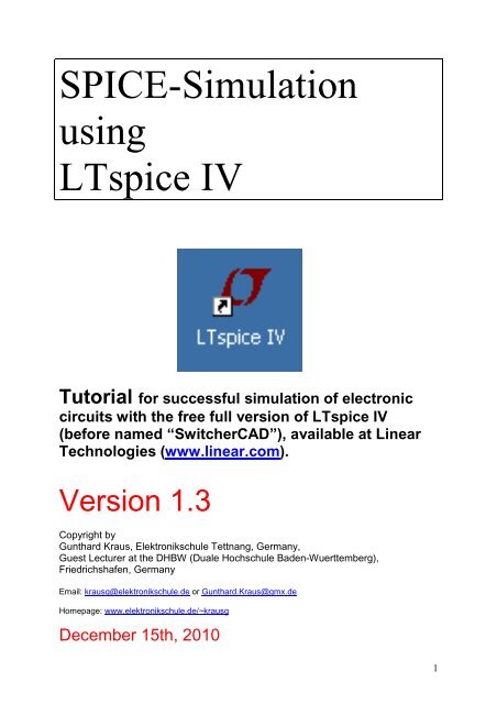
SPICE-Simulation using LTspice IV - von Gunthard Kraus
SPICE-Simulation using LTspice IV - von Gunthard Kraus
SPICE-Simulation using LTspice IV - von Gunthard Kraus

Create successful ePaper yourself
Turn your PDF publications into a flip-book with our unique Google optimized e-Paper software.
<strong>SPICE</strong>-<strong>Simulation</strong><br />
<strong>using</strong><br />
<strong>LTspice</strong> <strong>IV</strong><br />
Tutorial for successful simulation of electronic<br />
circuits with the free full version of <strong>LTspice</strong> <strong>IV</strong><br />
(before named “SwitcherCAD”), available at Linear<br />
Technologies (www.linear.com).<br />
Version 1.3<br />
Copyright by<br />
<strong>Gunthard</strong> <strong>Kraus</strong>, Elektronikschule Tettnang, Germany,<br />
Guest Lecturer at the DHBW (Duale Hochschule Baden-Wuerttemberg),<br />
Friedrichshafen, Germany<br />
Email: krausg@elektronikschule.de or <strong>Gunthard</strong>.<strong>Kraus</strong>@gmx.de<br />
Homepage: www.elektronikschule.de/~krausg<br />
December 15th, 2010<br />
1
Contents Page<br />
1. Introduction 5<br />
2. Installation 5<br />
3. Exercises with the included Example „Astable Multivibrator“ 5<br />
3.1. Using Schematic and <strong>Simulation</strong> 5<br />
3.2. Presentation of <strong>Simulation</strong> Results 7<br />
3.3. Deleting Curves 8<br />
3.4. Changing Curve Colours 9<br />
3.5. Changing the <strong>Simulation</strong> Time 10<br />
3.6. Changing Current- or Voltage Ranges 12<br />
3.7. Using Cursors 14<br />
3.7.1. Working with one Cursor 14<br />
3.7.2. Working with two Cursors 14<br />
3.7. Differential Measurements 15<br />
3.8. Current Measurements 16<br />
3.9. Changing Part Values 17<br />
4. Project 1: RC Lowpass Filter 18<br />
4.1. Drawing the Circuit Diagram with the Editor 18<br />
4.2. Changing Part Values 19<br />
4.3. Time Domain <strong>Simulation</strong>: non-repetitive Signals at the Input 20<br />
4.3.1. Step Response 20<br />
4.3.2. Switching ON and OFF 22<br />
4.3.3. Impulse Response 23<br />
4.4. Time Domain <strong>Simulation</strong>: <strong>using</strong> Periodic Signals at the Input 26<br />
4.4.1. Sine Wave (f = 1591 Hz) 26<br />
4.4.2. Square Wave (f = 1591 Hz) 27<br />
4.4.3. Triangle Wave (f = 1591 Hz) 28<br />
4.5. Frequency Domain simulation: AC Sweep 29<br />
5. FFT (= Fast Fourier Transform) 31<br />
6. Project 2: Rectifiers 34<br />
6.1. Simple Rectifier without Transformer 34<br />
6.2. Important: creating <strong>SPICE</strong> Model and Symbol for a Transformer 35<br />
6.2.1. The easiest Solution: a simple ideal Transformer 35<br />
6.2.2. Creation of the <strong>SPICE</strong> Model for a real Two Windings Transformer 35<br />
6.2.3. Creation of the Symbol for a Two Windings Transformer 35<br />
6.3. One Pulse Rectifier with Transformer 38<br />
6.4. Rectifier with Diode „1N4007“ 40<br />
6.5. Two Pulse Rectifier with Transformer 42<br />
7. Project 3: Three Phase AC-system 44<br />
7.1. Schematic and <strong>Simulation</strong> 44<br />
7.2. Rectifier Bridge for Three Phase AC Systems (= dynamo in a modern car or<br />
motorcycle) 45<br />
2
8. Project 4: U-I-Curves of Parts 47<br />
8.1. Resistor 47<br />
8.2. Diode 48<br />
8.3. NPN Transistor 49<br />
8.4. N Channel junction FET 51<br />
9. Project 5: Transistor Circuits 52<br />
9.1. One Stage Amplifier 52<br />
9.1.1. Time Domain <strong>Simulation</strong> 52<br />
9.1.2. Frequency Domain <strong>Simulation</strong>: AC Sweep 54<br />
9.2. Two Stage Broadband Amplifier with Feedback 55<br />
9.2.1. Task 55<br />
9.2.2. Circuit Diagram for <strong>Simulation</strong> 55<br />
9.2.3. Time Domain <strong>Simulation</strong> 56<br />
9.2.4. DC Bias 57<br />
9.2.5. Frequency Domain Dimulation: AC Sweep 59<br />
9.3. Parametric Sweep 60<br />
10. Project 6: OPA Circuits 62<br />
10.1. Starting with an Inverting Amplifier 62<br />
10.2. Preparing a <strong>SPICE</strong> Model from the Internet 62<br />
10.2.1. Gainblock for 1kHz to 30 MHz with OPA355 64<br />
10.2.2. <strong>Simulation</strong> <strong>using</strong> the selfmade OPA355 Subcircuit Model 64<br />
10.3. Usage of Labels 67<br />
11. Project 7: DC-DC Converters 69<br />
11.1. Model for the Power-MOSFET „IRFZ44N“ 69<br />
11.2. The Step Up Converter 71<br />
11.3. The Flyback Converter 73<br />
11.4. The Step Down Converter 75<br />
12. Project 8: Thyristor Circuits 77<br />
12.1. Thyristor Model 77<br />
12.2. Switching Resistive Loads 78<br />
12.3. Switching Inductive Loads 79<br />
12.4. Circuit with Gate-Transformer 80<br />
13. Project 9: Echos on Transmission Lines 81<br />
13.1. Transmission Lines -- only two Wires? 81<br />
13.2. Echoes 83<br />
13.3. <strong>Simulation</strong> of the Example with <strong>LTspice</strong> 85<br />
13.4. Open or Short Circuit at Cable’s End 88<br />
13.5. Lossy Cables (e. g. RG58 / 50Ω) 90<br />
13.5.1. How can I simulate a RG58 Coaxial Cable? 90<br />
13.5.2. <strong>Simulation</strong> of Cable Loss at 100MHz 91<br />
13.5.3. Feeding the RG58 Cable Entry with a Pulse Voltage 94<br />
13.5.4. A Short Circuit at RG58 Cables’s End 95<br />
14. Project 10: S-Parameters 96<br />
14.1. Echoes once again, but with more System (= S parameters) 96<br />
14.2. Example: 110MHz Tchebyshev Lowpass Filter (LPF) 99<br />
3
15. Project 11: Double Balanced Mixer 103<br />
15.1. Fundamentals and Informations 103<br />
15.2. The Ring Modulator 104<br />
15.3. The necessary Transformers 105<br />
15.4. DBM <strong>Simulation</strong> with ideal Transformers 106<br />
16. Project 12: <strong>Simulation</strong>s with Digital Circuits 108<br />
16.1. What you should know before 108<br />
16.2. Simple start: the inverter (= NOT) 109<br />
16.3. AND- and NAND-Gate 110<br />
16.4. D Flipflop 111<br />
16.5. Three Stage Frequency Divider with D Flipflops 112<br />
17. Project 13: Noise <strong>Simulation</strong> 113<br />
17.1. Fundamentals 113<br />
16.1.1. „Noise“ -- where does it come from? 113<br />
16.1.2. Other Sources of Noise 115<br />
16.1.3. Noise Temperature and Noise Factor for a Twoport System 116<br />
17.2. <strong>Simulation</strong> of the Spectral Noise Densitiy 116<br />
17.3. <strong>Simulation</strong> of the Noise Figure NF (in dB) 119<br />
18. <strong>Simulation</strong> of a Sine Oscillator 123<br />
19. Signals and Harmonics 128<br />
19.1. Fundamentals 128<br />
19.2. <strong>Simulation</strong> of a Single Pulse Spectrum 131<br />
19.3. <strong>Simulation</strong> of a Periodic Pulse Spectrum 133<br />
19.4. An Ideal Sine Wave 134<br />
19.5. The „One Side Clipped“ Sine Wave 135<br />
19.6. The Symmetrically Clipped Sine Wave 136<br />
20. The Secret of the Impulse Response 137<br />
20.1. First example: Dirac Pulse applied to a 160Hz RC Lowpass Filter 138<br />
20.2. Second Example: Dirac Test of a 110MHz Lowpass Filter (see Chapter<br />
14.2) 142<br />
20.2.1. Simulating S21 (= Forward Transmission) 142<br />
20.2.2. <strong>Simulation</strong> of S11 (= input reflection) or S22 (= output reflection) 147<br />
21. Modulation 149<br />
21.1. Principle of Amplitude Modulation (AM) 149<br />
21.2. Amplitude Shift Keying (ASK) 151<br />
21.3 Frequency modulation (FM) 152<br />
21.3.1. Generating an FM signal <strong>using</strong> the SFFM voltage supply 152<br />
21.3.2. Frequency Shift Keying (FSK) 154<br />
4
1. Introduction<br />
Modern electronics needs circuit simulation -- only in this manner you can save time, cost and effort when<br />
designing new or modifying existing circuits. Every new idea can be tested without a real printed circuit board or a<br />
soldering iron. Therefore the “<strong>SPICE</strong>” program was developed before 1980 at the Berkeley University, running on<br />
FORTRAN machines. But the more important version for the „normal“ user is P<strong>SPICE</strong> ( = <strong>SPICE</strong> for the PC).<br />
Around the „<strong>SPICE</strong> Kernel“ lot of people have programmed shells and programs for simple and intuitive usage<br />
and so you can find lot of software offers on the market. Most of the available programs are excellent, but huge<br />
and expensive and so we have to say „Thank You“ to Linear Technologies. They offer a free full <strong>SPICE</strong>-program<br />
named „<strong>LTspice</strong>“ without any restrictions. It was foreseen to simulate switching power supplies <strong>using</strong> the<br />
semiconductors of the enterprise…..but can also be used for nearly other electronic purpose. It can be<br />
downloaded from the web without any problems or fees but the usage is a little tricky -- a mixture of command<br />
lines, menues and mouse clicks. So it needs a lot of effort before the first own simulation. And this was the reason<br />
for an old professor like me to write this tutorial for other people.<br />
Warning for the new user:<br />
There are sometimes several ways to get to the same command (hot keys, menu bar symbols, menu selection,<br />
menus that appear with a right mouse click, etc.). So find out the way which you personally prefer and don’t be<br />
afraid of or confused by the different kinds of run commands.<br />
-------------------------------------------------------------------------------------------------------------------------------------------<br />
2. Installation<br />
No problem: download the zipped software from the homepage (www.linear.com), click on the „.exe“-file and you<br />
will be guided by the program. An icon is created at last on your Windows-screen.<br />
--------------------------------------------------------------------------------------------------------------------------------<br />
3. Exercises with the included Example „Astable Multivibrator“<br />
3.1. Using Circuit and <strong>Simulation</strong><br />
Click on „File“ in the upper left corner and then open „examples“.<br />
In the folder “educational” you find the file “astable.asc”. Open it.<br />
So the screen with the schematic should<br />
now look like.<br />
5
Now look for the button with the „running guy“. This starts the<br />
simulation.<br />
The simulation is<br />
done, but where are<br />
the results? (The<br />
diagram in the<br />
upper half of the<br />
screen is still<br />
empty....)<br />
If you prefer<br />
another manner of<br />
presentation, open<br />
the menu „Window“<br />
and click on „Tile<br />
vertically“.<br />
Better now for you?<br />
Information:<br />
Who likes a result plot with thick lines for the curves must now click on the<br />
“button with the hammer”. There he finds a menu ”Waveforms” and in it “Plot<br />
data with thick lines”.<br />
6
3.2. Presentation of <strong>Simulation</strong> Results<br />
Move the cursor to the point or line in the schematic of which you want to know the voltage. When arriving the<br />
cursor changes its form to a „testclip“. Now a simple mouseclick activates the presentation of the desired curve:<br />
You can continue in this manner, but remember: you have only one diagram. And how is it possible to separate<br />
the different curves of the different points? Where can you get the informations from? For instance so the<br />
presentation of all base- and collector-voltages looks like:<br />
In principle you have a choice of 3 possibilities:<br />
a) Look for the node’s name in the<br />
„Netlist“, because the different curves<br />
are named “V(node”). You find this<br />
important list in the menu “VIEW” and<br />
„<strong>SPICE</strong> Netlist“.<br />
This is the netlist for our example and<br />
easy to read. Every line belongs to a<br />
part in the schematic and begins with<br />
the part’s name, followed by the nodes<br />
between the part is inserted. At last you<br />
find the part’s value.<br />
7
) Much easier is the cursor method. Move the cursor to<br />
the desired point and look for the cursor’s change to a<br />
testclip.<br />
In this moment you get a message in the<br />
lower left corner of the screen with the<br />
node’s name<br />
-----------------------------------------------------------------------------------------------------------------------------------------------------<br />
voltage<br />
If necessary, repeat this procedure to get more diagrams.<br />
But how to delete undesired presented curves: see the following chapter!<br />
------------------------------------------------------------------------------------------------------------------------------<br />
c)<br />
Much easier is to<br />
use separate<br />
diagrams for the<br />
different curves.<br />
Right click right on<br />
the presentation<br />
window and choose<br />
„Add Plot Plane“.<br />
Now you get an<br />
additional diagram.<br />
Left click on it with<br />
the mouse to<br />
activate it.<br />
Afterwards click on<br />
the point in the<br />
schematic (f. i. the<br />
base of the left<br />
transistor) to<br />
present the desired<br />
3.3. Deleting Curves<br />
This is important to know if you present too much curves in only one diagram and you are loosing the overview.<br />
So<br />
a) Left click on the diagram to activate it -- the frame colour should change to a dark blue.<br />
b) Press F5 and the cursor will change to scissors.<br />
c) Move the scissors to the name of the undesired curve -- e. g. “V(n001)” above the diagram and click on<br />
it. The curve will disappear at once.<br />
Important:<br />
To measure another voltage in the schematic, please press at first „Escape“ on the keyboard to leave the delete<br />
function. Then click left on the schematic and watch that its frame changes to dark blue. If this is true, move the<br />
cursor to the desired point in the schematic until the form changes to a test clip…and so on....<br />
---------------------------------------------------------------------------------------------------------------------------------<br />
8
3.4. Changing Curve Colours<br />
A very simple exercise.......<br />
------------------------------------------------------------------------------------------------------------------------------------------<br />
9
3.5. Changing the <strong>Simulation</strong> Time<br />
This simple line ist the simulation command! It means::<br />
Simulate all signal curves from 0 to 25ms.<br />
(The simulation will always start at zero).<br />
If you now move the cursor to the text of this line<br />
and right click, then you’ll get this menu.<br />
Please enter a new value for “Stop Time” if you<br />
want a longer or shorter simulation time, press OK<br />
and finally the simulation button (with “the running<br />
guy” on it) to start P<strong>SPICE</strong>.<br />
Task:<br />
Please choose a stop time of 50ms and simulate the collector voltage V(n002) at the left transistor<br />
This should be the result.<br />
You can see that the simulation of the circuit behaviour after the start is a very important point -- e. g. for the<br />
analysis of switching power supplies (...and the parts, delivered by Linear Technologies...). But if you are only<br />
interested in the „steady state“, then you should use the zoom function.<br />
10
Task:<br />
Make the voltage curve visible between 30 and 35ms.<br />
Solution:<br />
a) Press this „enlarge button” and afterwards drag the region between 30 and 35ms<br />
with the pressed left mouse button.<br />
b) When releasing the<br />
mouse button you<br />
should see this diagram.<br />
c) If you want to go back to the full screen presentation press this<br />
button.<br />
------------------------------------------------------------------------------------------------------------------------------------------<br />
11
3.6. Changing Current or Voltage Ranges<br />
Very often you want to examine little details of a curve. So you have 2 possibilities:<br />
a) Use the discussed zoom function from chapter 3.4.<br />
b) Switch from “Autorange“ to „Manual Limits“.<br />
Example for solution a):<br />
Task:<br />
Show only the short negative „peak“ of the collector voltage by zooming:<br />
----------------------------------------------------<br />
Example for Solution b):<br />
Task:<br />
Set the values fort he vertical axis to the range 0…..+1.5V.<br />
Step 1:<br />
RIGHT click on the calibration of the vertical axis in the diagram<br />
and you get this menu for Manual Setting on BOTH AXIES.<br />
(Attention:<br />
If you left click on the axis scaling, you’ll only see the<br />
„quick solution menu”. Please test this, but we want to<br />
have a look on the „big solution” and continue with the<br />
case of the right mouseclick).<br />
Now switch off “Autoranging” and activate „Manual Limits“ .<br />
12
Step 2:<br />
Enter the new border values for the<br />
vertical axis.<br />
If you want you can also modify the<br />
horizontal time axis. But at this moment:<br />
let it be...<br />
This is the goal when returning to the full screen presentation including the schematic, where you now -- if you<br />
want! -- can modify part values.<br />
----------------------------------------------------------------------------------------------------------------------------------------------------<br />
13
3.7. Using Cursors<br />
3.7.1. Working with one Cursor<br />
Measuring the signal value at special points is easy with a cursor:<br />
If you now move the mouse to the marked point, you suddenly see the number of the cursor (here: „1“) hanging<br />
on your mouse. By “dragging” (= pressing the left mouse button + moving the mouse) it is possible to shift the<br />
cursor along the signal’s curve. The actual curve value is then indicated in the window.<br />
--------------------------------------------------------------------------------------------------------<br />
3.7.2. Working with two Cursors<br />
RIGHT click on the signal’s name and open „Attached Cursor“ in the menu:<br />
Now two cursors are<br />
visible and can be<br />
moved independently.<br />
The actual cursor<br />
values AND the<br />
differences are<br />
displayed in the<br />
window.<br />
14
3.7. Differential Measurements<br />
Every measured and presented voltage ist referred to a REFERENCE POINT (normally: ground). But how can we<br />
get the voltage between two points within the schematic? In this case you need a „differential voltmeter“, but<br />
where can you find that?<br />
Sorry:<br />
<strong>LTspice</strong> does not use a differential voltmeter like other <strong>SPICE</strong> programs!<br />
You must change the REFERENCE POINT for this purpose. That means that you<br />
at first must set a new reference point at one node and then click onto another<br />
node!<br />
So please open the menu „View“ and activate „Set Probe Reference”.<br />
Now we want to see the capacitor C1’s voltage (= base capacitor of the left<br />
transistor).<br />
After OK you now have a “testclip” as cursor. Click<br />
with it on the base of the left transistor.<br />
Then click on the collector of the right transistor (=<br />
other side of capacitor C1). That is all!<br />
Now use -- if you want! --<br />
the zoom function for<br />
interesting details.<br />
To leave this “differential<br />
measurement option” simply<br />
click on ESCAPE.<br />
------------------------------------------------------------------------------------------------------------------------------------------------<br />
15
3.8. Current Measurements<br />
Make the circuit diagram window active (...by a left mouseclick on it....) and move the cursor exactly over the<br />
part of which you want to know the current. The cursor changes to a “current sensor” and with a left mouseclick<br />
on the part you see the current curve.<br />
Example:<br />
Current in resistor R1 (= Collector resistor of the left transistor):<br />
----------------------------------------------------------------------------------------------------------------------------------------<br />
16
3.9. Changing Part Values<br />
Now we want to repeat the simulation with different part values. Let every capacitor be C = 1000pF and the both<br />
base resistors of the transistors R3 = R4 = 22kΩ.<br />
Move at every part the cursor exactly on its value indication and right click with the mouse. So you get the<br />
property menu and you can modify the value. Close with OK.<br />
….and this should be the simulation result:<br />
This is the new circuit to be simulated….<br />
Please use the zoom function or modify the simulation time to see the details or to measure the new oscillation<br />
frequency.<br />
------------------------------------------------------------------------------------------------------------------------------------------<br />
17
4. Project 1: RC Lowpass Filter<br />
4.1. Drawing the Circuit Diagram with the Editor<br />
Open a new file and save it in a new folder (e. g. named „RC-LPF_01“).<br />
Two tips:<br />
Then press the „resistor button“ to get the resistor, turn the<br />
symbol left with<br />
+ <br />
for 90 degrees an place it on your sheet. Leave this<br />
function either by a right mouseclick or by pressing<br />
„ESCAPE“ on the keyboard.<br />
Repeat this procedure for the capacitor and two ground<br />
symbols.<br />
a) To delete a part or a connection in the circuit, press F5. At once you get scissors as cursor.<br />
Move these scissors over the symbol (or the wiring connection) and left click: the part or the connection<br />
disappears at once.<br />
b) To move a part, press F7 and the cursor changes to a hand. Move this hand over the symbol<br />
of the part and left click . Now the part is connected to the cursor and can be moved with the mouse. A<br />
new left mouseclick will fix it in the new position.<br />
Do never forget:<br />
Leaving these special functions is done by pressing the ESCAPE KEY on the keyboard!<br />
We still need a voltage source and you must therefore<br />
open the „component list“ by pressing the special<br />
button.<br />
In the appearing list please look for „voltage“, mark it<br />
with a mouseclick and press OK. The symbol of the<br />
voltage source is then hanging on the cursor and can<br />
be placed within the schematic.<br />
Now we can start with wiring. Press the button with<br />
the pencil, roll the cursor to the start of the<br />
connection, click left and roll him to the other point.<br />
One more left mouseclick and the connection is<br />
perfect!<br />
Important:<br />
For an „edged“ wiring start as before, roll to the<br />
edging point and left click. Then you can do the<br />
rest of wiring in another direction.<br />
18
4.2. Changing Part Values<br />
This is demonstrated by capacitor C1:<br />
Move the cursor on the letter “C” and<br />
right click. Then enter the new value<br />
and close with OK.<br />
Please change the value of the<br />
resistor R1 to 10k in the same<br />
manner.<br />
So the circuit should now look like.<br />
But: before programming the voltage source we<br />
must decide wether we want a<br />
time domain<br />
or a<br />
frequency domain-<br />
simulation!<br />
----------------------------------------------------------------------------------------------------------------------------------------<br />
19
4.3. Time Domain <strong>Simulation</strong>: Non Repetitive Signals at the Input<br />
4.3.1. Step Response<br />
Please use a transient simulation in the time domain and let the input voltage jump in a very short time<br />
from 0 to +1V.<br />
Click on the button „Simulate“, then „Edit<br />
<strong>Simulation</strong> Command“ and „Transient“<br />
Enter a stop time of 2ms and check that this<br />
was accepted by filling the lower empty field<br />
with<br />
.tran 2ms<br />
Then press OK.<br />
.<br />
This command line hangs now on the cursor and must be placed by a<br />
mouse click somewhere in the Editor screen.<br />
To get the correct input voltage, right click on the symbol of the voltage<br />
aource to open the property window. There open the „ADVANCED“ –<br />
menu.<br />
The input voltage curve is generated by a series of linear lines<br />
(= „pieces“) between fixed points. This is done by the<br />
PWL = piecewise linear<br />
option, which now must be activated.<br />
At time1 = 0 the voltage is also 0V.<br />
At 1 ns the voltage value has risen to +1V<br />
and this value must not change.<br />
Please enter these two pairs of values in the list of the menu,<br />
make the information visible on the screen and close with OK.<br />
Place this information on the screen. Move it -- if necessary!<br />
-- by pressing F7, clicking on it and dragging with the mouse.<br />
Leave the F7 function by pressing the ESCAPE key on the<br />
keyboard.<br />
20
Now start the simulation, click on the input resp. output point in the schematic and admire the result:<br />
-----------------------------------------------------------------------------------------------------------------------------------<br />
21
4.3.2. Switching ON and OFF<br />
No problem because you have only to extend the value-pair list of the PWL source:<br />
0 0 (Zero Volt at start point)<br />
1n 1 (+1 Volt after 1 nanosecond)<br />
1m 1 (still +1 Volt during 1 millisecond)<br />
1.000001m 0 (Within 1 nanosecond back to 0V)<br />
Task:<br />
Add now the voltage at the resistor to this diagram!<br />
Solution: add a reference point to the output (= connection between the resistor and capacitor). Touch the<br />
connection between voltage source and resistor with the cursor and click. At once the desired resistor voltage is<br />
presented in the diagram.<br />
22
4.3.3. The Impulse Response<br />
Fourier, Fast Fourier and Laplace Transformations are important tools for modern Communication or Control<br />
Techniques. With these tools you can get all informations about the system’s reaction to any input voltage form --<br />
if you know the Transfer Function.<br />
This transfer function is the ratio of the output sine voltage to an applied input sine voltage, but<br />
presented in a complex “magnitude + phase” – form.<br />
So let us have a look at the impulse response:<br />
If you apply a „Dirac - Impulse“ to the input of an unknown system, then the answer (= Impulse<br />
Response) at the output will contain every information about this system -- because this answer is a<br />
“time domain form” of the transfer function.<br />
And with the transfer function you can -- by “convolution” -- calculate the output signal for every<br />
possible input signal.<br />
The Dirac Impulse is a little crazy: the amplitude is infinite, the pulse length is infinitely short...but the “pulse area”<br />
(= magnitude x pulse length) is “1”.<br />
This is impossible to generate but you can use a definite limited amplitude and a definite short pulse length --<br />
only be shure that you have again a pulse area of “1” and the pulse length is much shorter than the system’s time<br />
constant (....a factor of 100 to 1000 will do the job). And in real linear systems it is allowed to reduce the pulse<br />
magnitude to a value which is not dangerous for the system itself. Afterwards simply find out the necessary<br />
correction coefficient to get again the “ideal” values.<br />
Let us have a look at our lowpass filter.<br />
Task 1): Apply at the input of the LPF (R = 10kΩ, C = 10nF) a Dirac impulse with a peak value of<br />
Vampl = 1 Megavolt. Start with a delay time of 1 ms at an amplitude of 0V. Then the pulse rises to 1<br />
Megavolt within 1 Nanosecond, stays on this value for 1 Microsecond and decreases to 0V within 1<br />
Nanosecond.<br />
So we get a pulse area of<br />
1 Megavolt x 1Microsecond = 1Voltsecond<br />
Simulate the impulse response for a stop time of 2ms<br />
Task 2): Reduce the pulse amplitude to 100 Kilovolt but use a pulse length of 10 Microseconds to get again<br />
a pulse area of 1 Voltsecond. Simulate and compare the result with task 1.<br />
23
Solution for Task 1:<br />
First right click on the symbol of the<br />
voltage source to open the property<br />
menu. Then fill the PWL-list with<br />
the informations about the<br />
additional points and value pairs<br />
(use the button “Additional PWL<br />
Points”):<br />
0 0<br />
1m 0<br />
1,000001m 1000000<br />
1,001001m 1000000<br />
1,001002m 0<br />
When simulating input and output voltage you get this screen where only the Dirac impulse with its amplitude of 1<br />
Megavolt can be seen:<br />
Use the zoom function for other details, because the system’s response has only an amplitude of 10KV. So<br />
change the scaling of the two axis to see the response curve -- and afterward have a look at the solution on the<br />
following page.<br />
24
This is the correct presentation:<br />
------------------------------------------<br />
Solution for Task 2:<br />
Please be aware of the new pulse length (10 microseconds) and amplitude (100KV) and the modified PWL list in<br />
the property menu of the voltage source!<br />
--------------------------------------------------------------------------------<br />
25
4.4. Time Domain <strong>Simulation</strong> <strong>using</strong> Periodic Signals at the Input<br />
4.4.1. Sine Wave (f = 1591 Hz)<br />
We use a sine wave with a peak value of 1V at the corner frequency of this LPF. The corner frequency can be<br />
calculated in this manner:<br />
f Corner<br />
1<br />
1<br />
=<br />
=<br />
= 1591Hz<br />
2 • π •R<br />
• C 2 • π • 0.1ms<br />
Open the property menu of the voltage source by clicking on<br />
the source symbol and choose “SINE”. Then enter the<br />
following properties:<br />
DC Offset = 0<br />
Amplitude = 1 Volt (= peak value)<br />
Frequency = 1591 Hz<br />
Tdelay = 0 (= delay time after<br />
start)<br />
Theta = 0 (= damping factor.<br />
Enter zero for a constant sine wave)<br />
Phi = 0 (= start value of phase)<br />
Ncycles = 0 or empty field (this entry is<br />
important if you want to create a „Burst Signal“)<br />
Now open the „Simulate“ menu and „Edit <strong>Simulation</strong> Command“. Enter a stop time of 10 ms and then start the<br />
simulation. Check the values of 45 degrees of phase shift and an amplitude degration to 70% at the corner<br />
frequency on the screen.<br />
26
4.4.2. Square Wave (f = 1691 Hz)<br />
With a stop time of 4ms you get this result:<br />
Start with the properties of the voltage vource.<br />
For „PULSE“ we need the following entries:<br />
Vinitial = 0 (= minimum voltage value)<br />
Von = 1 Volt (= maximum voltage value)<br />
Tdelay = 0 (= delay after start)<br />
Trise = 1 Nanosecond (= rise time)<br />
Tfall = 1 Nanosecond (= fall time)<br />
Ton = 295,6 Microseconds (= pulse length)<br />
Tperiod = 591,3 Microseconds(= Period Time)<br />
Ncycles = 0 or empty field (= number of cycles<br />
when programming a burst signal)<br />
27
4.4.3. Triangle Wave (f = 1691 Hz)<br />
This is a little bit difficult, because we have to „strangulate“ the Pulse Source:<br />
If we choose a very long rise and fall time but a short pulse length then we get exactly that what we need: a<br />
triangle wave.<br />
This is the result for a stop time of 4ms:<br />
So please enter the following properties:<br />
Vinitial = 0 (= minimum voltage value)<br />
Von = 1 Volt (= maximum voltage value)<br />
Tdelay = 0 (= delay after start)<br />
Trise = 295,6 Microseconds (= rise time)<br />
Tfall = 295,6 Microseconds (= fall time)<br />
Ton = 1 Nanosecond (= pulse length)<br />
Tperiod = 591,3 Microseconds(= period time)<br />
Ncycles = 0 or empty field (= number of cycles<br />
for a burst signal)<br />
28
4.5. Frequency Domain <strong>Simulation</strong>: AC Sweep<br />
Please check now the generated simulation command:<br />
.ac dec 101 1 10k<br />
Step 1:<br />
Switch the voltage<br />
source to „AC<br />
Sweep“ by opening<br />
the property menu<br />
and the two entries:<br />
AC Amplitude = 1<br />
Volt<br />
AC Start Phase = 0<br />
Ignore the<br />
programming for the<br />
time domain of the<br />
last example and<br />
delete the mark in<br />
the field „Make this<br />
information visible on<br />
schematic“.<br />
Step 2:<br />
Open „Simulate“ and<br />
the line „Edit<br />
<strong>Simulation</strong><br />
Command“.<br />
Change to the „AC<br />
Analysis“ menu and<br />
enter:<br />
Decade sweep<br />
101 points per<br />
decade<br />
Start Frequency =<br />
1Hz<br />
Stop Frequency =<br />
10kHz<br />
29
Then start the simulation and test the result. Use the cursor to see the actual frequency, phase and magnitude.<br />
Congratulations, the first own example is now successfully terminated!<br />
30
5. FFT (= Fast Fourier Transformation)<br />
Very often we need information about all frequencies which can be found in a signal. It is a fact that only a pure<br />
sine wave consists of only one frequency. So, every deviation from the ideal sine wave curve produces new<br />
frequencies (harmonics) with frequency values of 2x, 3x, 4x….of the fundamental frequency. This information can<br />
be obtained by <strong>using</strong> the FFT.<br />
But first several things are neeeded to get the FFT working and to get good results.<br />
============================================================================<br />
The start frequency AND the minimum width of a spectral line AND the smallest frequency step are all<br />
determined by the<br />
Mimimum frequency step = start frequency = minimum line width =<br />
= 1 / simulation time<br />
Also for periodic signals the simulation time must be an integer multiple of the period time. If you ignore that you<br />
get “ghost lines“ and / or an additional noise floor.<br />
(An additional note for specialists only: you should reduce the used simulation time by one timestep. Otherwise<br />
you are already starting a new period which will not be complete. But this error is only noticeable for very “coarse<br />
time steps” or for a very small number of periods).<br />
===========================================================================<br />
Necessary properties of the maximum time step:<br />
a) Do not make it too coarse. This avoids „corners“ in the simulated time domain signal.<br />
b) The related „minimum sample frequency = 1 / maximum time step“ must have a minimum<br />
frequency value twice of the maximum frequency line in the simulated signal. Otherwise the „Nyquist -<br />
Shannon – Law“ is violated and you get undesired aliasing effects.<br />
c) The maximum frequency AND the dynamic range of a FFT are increased by the number of used<br />
samples in the FFT. But: these samples must be true and you must not use more samples for the FFT<br />
than you get from the time domain simulation. The number of samples can easily be calculated by<br />
True number of samples = simulation time / maximum time step<br />
===========================================================================<br />
<strong>LTspice</strong> uses data compression for the results file of the time domain simulation. This is undesirable because it<br />
looses informations and also a lot of the mentioned „true samples“.<br />
So switch off the data compression by the following Spice directive:<br />
.options plotwinsize=0<br />
==========================================================================<br />
For a FFT the number of used samples must always be a multiple of „2“.<br />
No problem because <strong>LTspice</strong> will always default to those in the choice menu.<br />
Note::<br />
More „true“ samples give a higher stop frequency AND an extended amplitude range in the simulated<br />
spectrum. But the necessary calculation time AND the resultant data file also increases.<br />
==========================================================================<br />
For specialists only.<br />
Because only the maximum time step is fixed, the sample rate applied by <strong>SPICE</strong> can vary or be increased<br />
automatically when simulating “the difficult parts of a curve”. But this cannot be forseen, equates to an additional<br />
FM and causes additional but unexpected spectral lines and an increased “noise floor” at high frequencies.<br />
This effect can be reduced by choosing the minimum sample rate as high as possible (= maximum time step as<br />
low as possible) and choosing as less samples for the FFT as possible.<br />
31
Example:<br />
Let us use the RC-LPF of the last chapter (R =10kΩ / C = 10nF). The input is fed by a symmetric square wave<br />
voltage (minimum amplitude value = 0V , maximum amplitude value = 1V , frequency = 1kHz).<br />
If we use a simulation time of 20ms with a maximum time step of 100ns we meet the above recommendations as<br />
follows:<br />
a) The simulation time of 20ms is an integer multiple of the signal’s period time (1ms).<br />
b) A maximum time step of 100ns is corresponding to a minimum sample frequency of 1/100ns = 10MHz.<br />
This gives a Shannon corner frequency of 0.5 x sample frequency = 5MHz.<br />
c) The number of true samples is 20ms / 100ns = 200 000. So we enter<br />
in the FFT menu.<br />
„131 072 sampled data points in time“<br />
Now draw the circuit, set the properties of the voltage source, choose simulation time and time step and write the<br />
directive to switch off the data compression.<br />
The time domain simulation result (= input and the output voltage) should be presented in two plot panes.<br />
Also “thick lines” are used for the curves (= button with the hammer / menu “waveforms”).<br />
Now right click on<br />
the input voltage<br />
and choose “View”<br />
and “FFT”<br />
32
This is the successful result:<br />
Select Input Voltage V(n001) by a mouseclick<br />
As discussed we have 200 000 real samples of this curve. So<br />
we enter a<br />
“number of 131 072 data point<br />
samples in time”<br />
and start the FFT.<br />
Start frequency = frequency resolution =<br />
50Hz = 1 / 20ms.<br />
The stop frequency is 3.3MHz and can only<br />
be increased by <strong>using</strong> a higher number of<br />
samples.<br />
Now change the diagram to linear vertical and<br />
horizontal result presentation to confirm theory<br />
which says:<br />
In a symmetric square wave you can only find the fundamental frequency and its odd harmonics.<br />
The amplitudes of the harmonics decrease exactly with their order:<br />
Note:<br />
If anybody is additionally interested in the phase information: click on the scaling of the right vertical<br />
diagram axis and press “Phase” in the menu.<br />
33
6. Project 2: Rectifiers<br />
6.1. Simple Rectifier without Transformer<br />
No problem: draw a circuit consisting of a Voltage Source, a diode and a resistor (1k). Now apply a sine wave (50<br />
Hz / peak value = 325 V) to the input and simulate from 0 to 100ms.<br />
Task:<br />
Add a parallel capacitor of 100 Mikrofarad to the output.<br />
Show also the diode current (by moving the cursor over the diode’s symbol to change the cursor into a<br />
current sensor).<br />
Solution:<br />
34
6.2. Important: creating <strong>SPICE</strong> Model and Symbol for a Transformer<br />
6.2.1. The easiest Solution: a simple ideal Transformer<br />
Sorry, but in the LTSpice part library you can’t find any transformer! So let us start with a simple but good solution<br />
found in the original <strong>SPICE</strong> manual:<br />
Place the necessary windings (with their Inductances) in the schematic and add a <strong>SPICE</strong> Directive for the<br />
magnetic coupling “kn” between these windings!<br />
Example for a two winding transformer and voltage transfer ratio<br />
= 1:1<br />
a) Place “Ind2” from the symbol library two times on the screen,<br />
because only at this symbol the start of the winding procedure is<br />
marked by a circle.<br />
b) The line “k1 L1 L2 1” says that the magnetic coupling factor<br />
between the windings L1 and L2 is “1” = 100%.<br />
c) Attention: It is not possible to enter a given voltage transfer ratio “(N1 / N2)” into<br />
P<strong>SPICE</strong>!!<br />
The reason is not complicated: P<strong>SPICE</strong> works always and only with parts and their properties (here: inductances<br />
and magnetic coupling factor). So we must use the inductances and the following relation:<br />
L<br />
L<br />
Primary<br />
Secondary<br />
⎛ N1⎞<br />
= ⎜ ⎟<br />
⎝ N2 ⎠<br />
2<br />
So choose a realistic value for L1 and then calculate L2 by <strong>using</strong> this formula.<br />
6.2.2. Creation of the <strong>SPICE</strong> Model for a real Two Windings Transformer<br />
We use the following transformer model for our work, which includes the „magnetic coupling“ between the primary<br />
and secondary winding, the flux leakage inductances, the winding capacitances and the copper resistors of the<br />
windings.<br />
Node 1 and 2 are the<br />
primary winding<br />
connections, node 3<br />
and 4 the connections<br />
for the secondary<br />
winding of the model<br />
for the simulation.<br />
For the “inner nodes”<br />
you should choose<br />
much higher numbers<br />
to avoid collisions<br />
when “blowing up the<br />
circuit diagram” with<br />
more windings ore<br />
parts.<br />
35
Now have a look at the following <strong>SPICE</strong> – Model, <strong>using</strong> the subcircuit „xformer_01“ with its connections<br />
1 / 2 / 3 / 4:<br />
(Lleak is the name for the flux leakage inductances which represent the part of the flux who does not run<br />
through both main inductances leaded by the magnetic core of the transformer. All other circuit elements<br />
correspond to the above diagram):<br />
*<br />
* [1] ---. ||<br />
* ) || .--- [3]<br />
* ) || (<br />
* ) || (<br />
* [2] ---. || .--- [4]<br />
*<br />
.SUBCKT xformer_01 1 2 3 4<br />
*<br />
** Primary<br />
Lleak1 1 20 1mH<br />
Lpri1 20 21 1H<br />
Rpri1 21 2 1<br />
Cpri1 1 2 20pF<br />
*<br />
* *Secondary<br />
Lleak3 3 22 1mH<br />
Lsec1 22 23 1H<br />
Rsec1 23 4 1<br />
Csec1 3 4 20pF<br />
K Lpri1 Lsec1 0.999<br />
.ENDS<br />
Explanation:<br />
Every line starts with the name of the part, followed by the numbers of the nodes between this part is inserted in<br />
the circuit. And at last you find the parts value.<br />
In praxis the magnetic coupling is always below „1“ (due to the flux leakage). So always insert a value smaller<br />
than 1 (here: k = 0.999). Some <strong>SPICE</strong> versions start a protest action if you don’t follow this advice.<br />
Primary and secondary winding use the same number of turns. So you have to enter the same inductance value<br />
to get a 1:1 - transformer.<br />
Note:<br />
The description of the circuit starts always with .SUBCKT …………… and ends with .ENDS<br />
================================================================================<br />
Very important:<br />
a) The finished model is named xformer_01.lib an should be saved in the folder<br />
Programs / LTC / <strong>LTspice</strong><strong>IV</strong> / lib / sub<br />
where all other LTC-<strong>SPICE</strong>-models are already located. Please pay attention to the correct path and the correct<br />
extension when saving this file...…<br />
b) It is impossible to enter the turn ratio! The only possibility is to enter different primary and secondary main<br />
inductances and we’ll handle this in the next project.<br />
================================================================================<br />
36
6.2.2. Creation of the Symbol for a Two Windings Transformer<br />
Step 1:<br />
Open „File“ and click on „New Symbol“. Now you see an empty screen with “cross and circle” in its center.<br />
Step 2:<br />
Open „DRAW“, choose „Rect“ (= rectangle) and draw it with the<br />
dimensions 20mm x 20mm around the symbol’s center point<br />
(…as a help: You find a fine point grid with 5mm distance on the<br />
screen).<br />
(The red circles at two corners of the rectangle are „capture<br />
points“ for the user when placing this symbol in a circuit).<br />
Step 3:<br />
Go to „Edit“ and „Add Pin / Port“ to generate the connection<br />
points. But in the menu you have at every connection point not only<br />
to enter the pin Number BUT ALSO the relative position between<br />
this point and the Point’s Label.<br />
And always examine carefully whether the point’s label and<br />
netlist order are identical!<br />
Then click OK and you have the pin at your cursor. Now you can<br />
place it in a distance of 5mm from the symbol (See next figure).<br />
Step 4:<br />
Generate all 4 Pins and afterwards open once more „DRAW“ to connect the<br />
pins to the symbol by wires.<br />
So the terminated symbol should look like.<br />
Step 5:<br />
Let us complete the real transformer for the simulation. Please<br />
open „EDIT / Attributes / Edit Attributes“ to arrive at this menu.<br />
Now enter all entries as given in the figure.<br />
(Remark: Prefix „X“ means a subcircuit).<br />
Warning:<br />
The line for „Value2“ MUST NEVER BE EMPTY ---<br />
otherwise you can get a cryptic error message!<br />
Normally use the same entry as in the line for the<br />
spice model, but without extension.<br />
37
Step 6:<br />
At last make visible all important informations for the user.<br />
Start with „Edit“ and „Attributes“, but now choose „Attribut<br />
Window“. When clicking on „value“, then you get the description<br />
„2_wind_XFRM“ at your cursor and you can place it over the<br />
symbol.<br />
Then repeat the procedure but now choose „SpiceModel“ =<br />
xformer_01.lib and place it below the symbol. The work is done!<br />
Step 7:<br />
Save the complete symbol.<br />
Open „File“ and „Save as“ and the correct path starting at „SwCADIII“ and „lib“ just down to the folder „sym“<br />
(= symbols). There create a new folder named „Xformers“ and save this new part as „xformer_01.asy“.<br />
6.3. One Pulse Rectifier with Transformer<br />
Now let us test a circuit with line transformer, one pulse-rectifier and output capacitor.<br />
Task:<br />
Test a power supply consisting of a line transformer, rectifier, load resistor R1 = 1kΩ and load capacitor<br />
C1 = 100µF. Line input voltage is 230Vrms / 50 Hz, the turn ratio of the transformer is 20:1. Simulate in the<br />
time domain from 0...200ms.<br />
Solution:<br />
Most of the necessary parts are<br />
already known from the last<br />
example. Fetch and place them,<br />
wire and enter the correct part<br />
values including the properties of<br />
the voltage source and add the<br />
command for the simulation from 0<br />
to 200ms in the time domain.<br />
But now we need the line<br />
transformer of the last chapter.<br />
Fetch and place the part.<br />
Then we look for the necessary<br />
transformer property entries.<br />
You cannot enter the turn ratio N1/N2 in a direct form, so you need the following equation for the inductances:<br />
L<br />
L<br />
primary<br />
secondary<br />
⎛ N<br />
= ⎜<br />
⎝ N<br />
1<br />
2<br />
⎞<br />
⎟<br />
⎠<br />
2<br />
Let us apply a value of 1Henry for the primary main inductance (….ideal transformer…) and calculate the<br />
secondary main inductance for a turn ratio of 20:1 in the following manner:<br />
L<br />
=<br />
primary<br />
L secondary<br />
2<br />
( 20)<br />
=<br />
1H<br />
400<br />
= 2.5mH<br />
38
For an ideal transformer you can reduce the values for<br />
the flux leakage inductances, the copper resistors and<br />
the winding capacitances.<br />
But always you must never set them to zero”......<br />
Especially a resistor of zero<br />
Ohms in series to an inductance<br />
causes in a “normal <strong>SPICE</strong><br />
version” at once an error<br />
message or a simulation abort!<br />
So this model file of the transformer is a good template<br />
for your work. Open the „xformer_01.lib“ – File, change<br />
the entries and save it.<br />
Now the simulation runs and here you have the result screen with the voltages at the left and the right side of the<br />
diode:<br />
39
6.4. Rectifier with Diode 1N4007<br />
We want to use the well known universal line rectifier diode 1N4007 instead of the ideal diode.<br />
Sorry; but the <strong>SPICE</strong>-model of this type cannot be found in the LTC-library…<br />
So let us tackle the import of foreign models (from the WEB.....).<br />
Step 1:<br />
Use Google and look for diode.lib<br />
(This is an ORCAD-library with a lot of rectifiers).<br />
But be carefully:<br />
You get this library as a HTML-file and you must not use it in this form!!!!!<br />
So mark the content by + , copy to the clipboard by + and insert it into a new file of a<br />
text editor (like Notepad).<br />
Now save this file as „diode.lib“ in the folder<br />
LTC / <strong>LTspice</strong><strong>IV</strong> / lib / sub<br />
(But pay attention to get the correct extension „*.lib“ by choosing the type “all files”. Otherwise the editor will add<br />
a further extension “*.txt” and the library cannot be found by our program…)<br />
Step 2:<br />
Now open „diode.lib“ with the text editor and<br />
search for „1N4007“. You will then recognize<br />
that the correct diode model name is<br />
D1N4007<br />
Step 3:<br />
Move the cursor on the letter „D“ at the symbol of<br />
the diode and right click with your mouse.<br />
Then enter the new correct value „D1N4007“ and<br />
close by pressing OK.<br />
Step 4:<br />
Enable the program to find out the correction location of this D1N4007 model and add the following Spice<br />
directive on the screen:<br />
.include diode.lib<br />
40
Step 5: self-explainig….<br />
41
6.5. Two Pulse Rectifier with real Transformer<br />
Here we need at first something new: a line transformer with 2 secondary windings.<br />
Step 1:<br />
We open our well-known file „xformer_01.lib“ to modify it.<br />
Let the turn ratio be again 20:1 and add an additional<br />
secondary winding, also with 2.5mH. Write the necessary<br />
lines in your file (...they are a simple copy of secondary<br />
winding 1, but be aware of the node names...)<br />
Reduce the flux leakage inductances and the copper<br />
resistors to get an ideal transformer, but don’t set them to<br />
zero.<br />
Please do not forget:<br />
No we have 3 windings which are magnetally coupled.<br />
You have to enter a new coupling information<br />
K Lpri1 Lsec1 Lsec2 0.999<br />
At last save the file as „xformer_02.lib“ in the “sub“folder<br />
of the library.<br />
Step 2:<br />
Also a new symbol is necessary and must be created -- see<br />
Chapter 6.2.2.<br />
But do not forget:<br />
Warning:<br />
The line for Value2 MUSS NEVER BE<br />
EMPTY....otherwise you can get a cryptic<br />
error message and / or a simulation<br />
abort...<br />
Step 3:<br />
Draw the circuit <strong>using</strong> the new transformer and two diodes of the 1N4007-type. Then simulate and compare the<br />
result with the following page:<br />
42
-------------------------------------------------------------------------------------------------------------------------------------------------<br />
43
7. Project 3: Three Phase AC System<br />
7.1. Schematic and <strong>Simulation</strong><br />
We need 3 voltage sources, 3<br />
transformers and 3 load resistors<br />
to review this technique.<br />
For the transformers we will use<br />
our well-known file<br />
„xformer_01.lib“,<br />
but in this case choose<br />
identical main<br />
inductances on the<br />
primary and secondary<br />
side to get a turns ratio of<br />
1:1.<br />
Fetch all these parts from the<br />
library and draw the circuit<br />
diagram.<br />
Then move the cursor over the symbol of<br />
every voltage source and right click. All<br />
entries for the 3 sources are identical<br />
(except one....):<br />
DC offset = 0 Volt<br />
Amplitude = 325 V (peak value for<br />
RMS = 230V)<br />
Frequency = 50 Hz<br />
Phi = 0 degrees (start phase of the sine<br />
curve)<br />
Important:<br />
The 3 voltages have the same amplitude<br />
and the same frequency, but differ in the<br />
phase shifts. We cannot enter the<br />
necessary phase difference of 120<br />
degrees in the property menu -- so<br />
simply enter different start delays:<br />
for V1 the delay time is 0ms<br />
for V2 the delay time is 6,66666 ms<br />
(see figure)<br />
for V3 the delay time is 13,33333ms<br />
44
When simulating for 200ms, you will get the following result:<br />
-----------------------------------------------------------------------------------------------------------------------------------------<br />
7.2. Rectifier Bridge for Three Phase AC Systems (e. g. Dynamo in a modern<br />
Car or Motorcycle)<br />
Save this circuit in a new project folder and give it an appropriate name. Then modify the circuit by adding 6<br />
diodes (1N4007). Delete two of the three resistors and wire the circuit as shown:<br />
If you now simulate, you will get the following result for the input voltage V1 and the output voltage at R1:<br />
45
------------------------------------------------------------------------------------------------------------------------------------------<br />
46
8. Project 4: V-I-Curves of Parts<br />
8.1. Resistor<br />
A resistor is the best object to make visible the V-I curve of a part.<br />
So open a new project and draw the schematic.<br />
For the resistor R1 choose a value of 1kΩ.<br />
Then open the property menu of the voltage source (by a right<br />
mouseclick on the “+”-sign in the symbol) and enter in the right upper<br />
corner of the menu “0” (= Zero Volts) as DC-Value.<br />
Check the schematic for its correctness.<br />
In the simulation menu open<br />
„Edit <strong>Simulation</strong> Command“<br />
and fill in the following DC-Sweep-entries for<br />
the voltage source V1:<br />
Start Value = 0 Volts<br />
Stop Value = 10 Volts<br />
Increment = 1Volt<br />
Linear Sweep<br />
Please check the so generated simulation<br />
command „.dc V1 0 10V 1V “ in the<br />
lower part of the window.<br />
Then close with OK<br />
and start the<br />
simulation.<br />
Move the cursor<br />
to the upper<br />
connection of the<br />
resistor R1.<br />
When the cursor<br />
suddenly looks like a<br />
“current sensor”: left<br />
click and you get this<br />
screen.<br />
47
8.2. Diode<br />
This is now a very simple exercise:<br />
First save the project under a new name. Then delete the resistor (key F5) and replace it by a diode (= part<br />
„diode“ in the Library).<br />
At last modify the simulation command to<br />
.dc V1 550mV 750mV 10mV<br />
Now the voltage range is 550mV to 750mV with an increment of 10mV. This is the optimum for a silicon diode.<br />
48
8.3. NPN Transistor<br />
In the „example“ folder of the program you will find a very nice example „curvetrace.asc“ for this purpose:<br />
You can see:<br />
a) A DC voltage source V1 is connected to the collector of the transistor. The voltage start value is “0”.<br />
b) A current source I1 with start value „0“ feeds the base of the transistor.<br />
The simulation command<br />
.dc V1 0 15 10mV I1 0 100u 10u<br />
means:<br />
Increment voltage V1 from 0 Volts to +15 Volts in steps of 10mV. Use this voltage for the horizontal axis in<br />
the waveform viewer .<br />
Then apply a base current between 0 and 100 Microamperes (incremented by steps of 10 Microamperes)<br />
and write the simulated curves into the waveform viewer.<br />
Move the cursor<br />
to the collector of<br />
transistor Q1.<br />
When the cursor<br />
suddenly looks like a<br />
“current sensor”, left<br />
click and you will get this<br />
screen.<br />
49
If you are interested in the relation between collector current and base voltage, then you need this schematic:<br />
a) Replace the base current source with a voltage source. Start value is “0”.<br />
b) Modify the simulation command to:<br />
.dc V1 0 15V 10mV V2 650mV 750mV 10mV<br />
The voltage source V1 stays the same. The base voltage V2 is stepped from 650mV to 750mV by increments of<br />
10mV.<br />
That is all. See the result in the waveform viewer on the top right of this page....<br />
50
8.4. N-Channel Junction FET<br />
First we have to replace the NPNTransistor of the last example by the FET (= part „njf“ in the part library of the<br />
program). To show the example to its best we will use the well known<br />
BF245B<br />
First search on the internet with the Google entry<br />
bf245b spice model<br />
Copy the content of the result to the clipboard and then into a new editor sheet. Save this sheet as<br />
BF245B.mod<br />
in the folder „sub“ of the program’s part library.<br />
And then do the following:<br />
First select the N-Channel Junction FET symbol from the library (= „njf“) and place it on the schematic. Then right<br />
click on the model description „NJF“ beside the symbol. Change it to BF245B and finally add a <strong>SPICE</strong> directive to<br />
the schematic:<br />
.include BF245B.mod<br />
Now the software will use the downloaded BF245B model for the simulation.<br />
Lastly the gate voltage range must be altered. For a normal junction FET it is the best to use a range from<br />
-5V to 0V in Steps of 100mV<br />
The simulation should now run without any problems.<br />
51
9. Project 5: Transistor circuits<br />
9.1. One Stage Amplifier<br />
9.1.1. Time Domain <strong>Simulation</strong><br />
Procedure:<br />
Step1:<br />
Place 4 resistors, 1 capacitor, 2 voltage sources, 1 npn-transistor and wire.<br />
Step 2:<br />
Enter the correct values for the resistors and the capacitor.<br />
In the upper voltage source V2 choose „DC“ with an amplitude of +12V.<br />
The lower voltage source V1 must be programmed as a sine wave with Vpeak = 100mV and 1kHz.<br />
Step 3:<br />
Simulate from 0 to 10ms.<br />
We need a power<br />
supply, a sine<br />
voltage source,<br />
one capacitor, four<br />
resistors and an<br />
npn-transistor.<br />
Let’s start!<br />
Step 4:<br />
Start the search engine and look for BC547B.lib“ on the internet. The content of the found html-file must be<br />
marked, copied to the clipboard and inserted into a new sheet of a text editor. Save the file as „BC547B.lib“ in the<br />
folder<br />
LTC / <strong>LTspice</strong><strong>IV</strong> / lib / sub<br />
Step 5:<br />
Move the cursor to the information „NPN“ beside the transistor’s symbol, click right and enter the correct<br />
information „QBC547B“ (...because this is the same as the name of the Transistor’s model file in “BC547.lib”) and<br />
add the spice directive .include BC547.B to your schematic.<br />
52
In the simulation we would like to see the input voltage, the base and the collector voltage of the transistor.<br />
Please verify the phase shift of 180 degrees caused by the transistor.<br />
Also we can test the “ predicted gain” for such a stage, given by the simple equation<br />
VU = RC / RE = 470 / 100 = 4,7<br />
(to check this please measure the amplitude of the output voltage and calculate the ratio with the input voltage’s<br />
amplitude of 100mV).<br />
53
9.1.2. Frequency Domain <strong>Simulation</strong> (“AC Sweep”)<br />
Step 1:<br />
Change the properties of voltage source V1 to “AC-Sweep”<br />
by entering the values “1” for the AC Amplitude and “0” for<br />
the AC Phase.<br />
Make the information visible on the schematic.<br />
Step 2:<br />
Open „Simulate“ and „Edit <strong>Simulation</strong> Command“ to get<br />
this menu. In „AC Analysis“ please enter the values for a<br />
decade sweep with 101 points per decade from 1 Hz to<br />
200MHz.<br />
So the simulation result should look like this:<br />
54
9.2. Two Stage Broadband Amplifier with Feedback<br />
9.2.1. Task<br />
Design a gainblock for a 75Ω communication system with the following specifications:<br />
a) Input and output resistance are both 75Ω. So a lot of 75Ω blocks can be connected in series <strong>using</strong> the<br />
RG59 cable type.<br />
b) The gain should be 6dB when loading the output by 75Ω.<br />
c) Use a power supply with +12V DC.<br />
d) The gain must be constant in the frequency range from 1kHz to 10MHz.<br />
e) Use an npn and a pnp transistor (BC547B and BC557B) with feedback.<br />
f) Use a trimmer resistor in the base circuit of the first transistor to compensate all part tolerances.<br />
9.2.2. Circuit Diagram for <strong>Simulation</strong><br />
Draw this circuit and take note:<br />
The values of the resistors R1 and R2 must always be written as<br />
14.8k and 2.2k<br />
Never write 14,8k or 2,2k -- you will get wrong results without any warnings!!<br />
55
The npn transistor BC557B is not included in the LT’s library, so you need the internet again. When youhave<br />
found the model file, copy it into an editor’s new file (do you remember? You receive a HTML file) and save it in<br />
the library folder.<br />
Note: When you have found the model files the transistors are named QBC547B and QBC557B. Use these<br />
names in the spice directive and in the schematic.<br />
The input voltage is a sine wave with a peak value of 100mV and a frequency of 1kHz. <strong>Simulation</strong> time is 0….10<br />
Milliseconds.<br />
Something new is the command „.op“<br />
With this command you get information about the DC-values in the circuit (= „DC operating point“). The<br />
information is presented in form of a list.<br />
The test points in the schematic are the voltage source V1 and the termination resistor R9 (75Ω) at the output.<br />
9.2.3. Time Domain <strong>Simulation</strong><br />
As required the output voltage’s peak value is twice that of the input voltage and that gives a gain of 6 dB……<br />
Two common emitter stages produce a phase shift of 2 x 180 = 360 degrees. So the output voltage is again in<br />
phase with the input voltage.<br />
56
9.2.4. DC Bias<br />
If you want to know the DC-Currents and DC-Voltages for the operating point, then you should do this:<br />
1) Open „<strong>Simulation</strong>“ and „Edit <strong>Simulation</strong> Command“.<br />
2) Change to „DC op point“<br />
3) In the window you should now find „.op“<br />
4) Confirm this by pressing OK and test, whether<br />
5) the command „.op“ is now connected to the cursor. if it is then it can be placed on the schematic. (Youcan<br />
check this as the „Tran“-Command will now start with a semicolon ( ;tran 10ms )?<br />
Now press the<br />
simulation button (with<br />
the running guy) and<br />
wait for the result.<br />
This is what it looks like<br />
and you can examine<br />
the current / voltage list.<br />
Now close the list because there is an easier way to get every current- or voltage value (See next page):<br />
57
Note:<br />
To return to the transient simulation, please replace the point in the .op simulation command by a<br />
semicolon. Also replace the semicolon in the ;tran command by a point.<br />
But the fastest way is <strong>using</strong> the path „<strong>Simulation</strong> / Edit <strong>Simulation</strong> Command / Transient”. There click OK and<br />
this operation will be automatically done by the software.<br />
58
9.2.5. Frequency Domain <strong>Simulation</strong>: AC Sweep<br />
No problem:<br />
Open the property menu of the voltage source V1, enter „1“ for the AC-amplitude, „0“ for the AC-phase and a new<br />
simulation command for an AC-sweep from 1Hz to 200MHz with 101 points per decade:<br />
59
9.3. Parametric Sweep<br />
If you have a look at “<strong>LTspice</strong> / Dot Commands“ in the online help, then you will find a lot of commands and<br />
capabilities.<br />
Let us test the <strong>SPICE</strong>-command .step<br />
This is important because with „step“ you can automatically vary the value of a part or a voltage and repeat the<br />
simulation.<br />
Let’s take the circuit of the last section and vary the upper resistor R1 in the base voltage divider in 5 steps from<br />
10k to 15k. This will enable you to get the optimum operating point.<br />
Note:<br />
a) The peak value of the input voltage is now 0.3V<br />
b) The value of R1 is replaced by the variable {Rx}<br />
c) With the spice directive .step param Rx 10k 15k 1k the value of Rx is<br />
increased from 10k to 15k in steps of 1k.<br />
Now press the simulation button ( the “running guy”). The simulation will run, but you don’t see any results. So<br />
move your cursor to the collector of the transistor Q2 and click.<br />
60
You will see this result and that a value of approx. 15k for R1 (= lowest curve) will do the job perfectly (and give a<br />
VDC = +6.5V at the collector of Q2)<br />
61
10. Project 6: OP Amp Circuits<br />
10.1. Let us start with an Inverting Amplifier<br />
Let us have a look at a simple OP Amp circuit <strong>using</strong> one of the LT models which come with the software.<br />
Task:<br />
To simulate an inverting amplifier with the „LT1001“ to have the following specifications:<br />
Gain = 10 (= 20dB)<br />
Input Resistance = 1 kΩ<br />
Use two power supplies with +15V and -15V<br />
The input signal is a sine wave with a peak value of 1V and a frequency of 1kHz. Simulate the input and<br />
output voltage from 0...10ms.<br />
Solution:<br />
You see, as predicted by theory, that there is a phase shift of 180 degrees between input and output.<br />
Additional task:<br />
Use an AC sweep to determine the frequency response and the upper cutoff frequency. Simulate up to<br />
1MHz.<br />
Solution:<br />
In the properties of the voltage source V3 set AC amplitude = 1 and AC phase = 0<br />
.<br />
Then write the simulation command<br />
.ac dec 101 1 1MEG<br />
for a decadic sweep with 101 points per decade from 1 Hz to 1MHz.<br />
62
Using the cursor you will find the corner (= cutoff) frequency at 75.6kHz. Here the gain has decreased by -3dB.<br />
63
10.2. Preparing a <strong>SPICE</strong> Model from the Internet<br />
When doing your own development work you often need a special circuit from a manufacturer. Most companies<br />
offer their <strong>SPICE</strong> model collection free of charge on the Internet. So search for and use them!<br />
Modern OP Amps can work up to 500MHz and more - even the circuit’s noise can be simulated. Let us use such<br />
a modern part in a simulation and learn how to create a symbol for a downloaded complex circuit.<br />
----------------------------------------------------------------------------------------------------------------------------------<br />
10.2.1. Gainblock for 1kHz to 30 MHz with OPA355<br />
The OPA355 is a modern low noise OP Amp with a cutoff frequency of 200MHz (there the gain has decreased to<br />
1). We want to create a „gainblock“ for a 75Ω – system with it.<br />
Specifiations:<br />
a) Only one power supply with +5 V (= maximum Vcc value). Therefore the mean output DC voltage must<br />
be set to +2.5V.<br />
b) Gain = 4 for an unloaded output, but gain = 2 with a terminated output pin.<br />
c) Input resistance = output resistance = 75Ω.<br />
d) Lower corner frequency = 100 Hz. Upper corner frequency = 50 MHz for a gain reduction of 0.5dB.<br />
e) Use a non inverting circuit.<br />
-----------------------------------------------------------------------------------------------------------------------<br />
10.2.2. <strong>Simulation</strong> <strong>using</strong> the selfmade OPA355 Subcircuit Model<br />
The necessary <strong>SPICE</strong> model can be found as „sbom143.zip“ in the Texas Instruments homepage. After dezipping<br />
save it as „OPA355.mod“ in the well-known library folder „lib / sub“.<br />
Once more you have to create a new symbol (See<br />
chapter 6.2.3).<br />
Be aware of the additional ENABLE pin. In the<br />
schematic this pin must be connected to the supply<br />
voltage (+5V):<br />
This should be the result....<br />
…and this is the correct attribute list. Only with these<br />
entries will everything run well.<br />
Warning:<br />
The value for the attribute<br />
“Value2” MUST NEVER BE<br />
EMPTY!!!<br />
(…the best is to use the <strong>SPICE</strong><br />
model name…)<br />
If this entry is missing, then you<br />
can get cryptic error messages<br />
and the simulation aborts…<br />
64
Let us now draw the complete circuit:<br />
Explanations:<br />
a) The +5V supply must be connected to the pins „+Ub“ and „Enable“. Also the voltage divider (consisting<br />
of R1 and R2) must be connected to +5V to get the necessary +2.5V at the input pins.<br />
b) R5 gives the input resistance of 75Ω, R6 the output resistance of 75Ω.<br />
c) R4 and R3 form a feedback network. So the „non-inverting function“, and an unloaded gain =4 and a<br />
loaded gain = 2 ( +6dB) are realised<br />
This is the result of the simulation for the output voltage at R7:<br />
Fine!<br />
65
And something interesting is to feed the circuit with a pulse voltage (peak value = 0.5V / frequency = 10MHz):<br />
Very nice, indeed<br />
------------------------------------------------------------------------------------------------------------------------------<br />
66
10.3. Use of Labels<br />
In general OP Amp circuits need a positive and a negative supply voltage. The fully drawn circuit then gets a little<br />
bit untidy, so applying some Labels simplifies the appearance.<br />
When <strong>using</strong> a label you replace the wiring by a simple connection with a name for the node at all points where it is<br />
needed and you no longer need to draw all the necessary wires.<br />
Let us use the OPA355 from the last chapter and build a new gain block (gain = 10 (+20dB) ; non- inverting<br />
circuit; 2 supplies of +2.5V and -2.5V).<br />
Also use a label for the input and for the output nodes.<br />
This has another advantage:<br />
In the waveform viewer you now get the label as information for the trace<br />
instead of the node number....<br />
So the schematic looks like this, preset for a sweep from 1Hz to 200MHz:<br />
And now let us do the work, starting with the 2 power supplies.<br />
Step 1:<br />
Delete all wiring between the power supply and the circuit and press the “label button”:<br />
67
Step 2:<br />
Now enter +2.5V in the field and click on OK.<br />
The label “hangs” on the cursor and can be placed on the schematic and<br />
wired.<br />
Note:<br />
Before placing the label, it looks like a huge rectangle<br />
with an additional little rectangle on the centre of the<br />
lower edge. This little rectangle is the “catching<br />
point” and must be connected to the symbol of the<br />
power supply!<br />
Step 3:<br />
Now click and place the label at every point in the schematic which needs the +2,5V supply.When all the<br />
instances are placed then connect each one to the corresponding circuit point.<br />
Note: if wires are already present the labels can be placed directly on the wire <strong>using</strong> the “catching point” and they<br />
will automatically be connected.<br />
Repeat steps 2 & 3 for the “-2.5V supply<br />
------------------------------------------------------<br />
Lastly, repeat this procedure to place the „input“- and „output“ labels.<br />
But please note:<br />
The input of the OP Amp needs the label „INPUT“-- but select the Port<br />
Type as „Input”.<br />
The output of the OP Amp needs the label “OUTPUT” -- but select the<br />
Port Type as “Output”.<br />
And this is the sweep result (only gain, without phase):<br />
68
11. Project 7: DC-DC Converters<br />
First a warning:<br />
These circuits use complex simulations and realistic inductance properties because an oversimplified inductor<br />
model will cause errors or simulation aborts in many applications. Very expensive simulation software versions<br />
use special (and secret) tools to avoid these problems, but we have only the normal Berkeley <strong>SPICE</strong> kernel......<br />
With the following rules you can avoid most of these problems:<br />
a) Never use an ideal inductance -- always add a series resistor (even 0.01Ω can do the job!).<br />
b) Every inductor has a winding capacitance, and often the circuit has additional stray capacitance. This<br />
always gives resonance effects with (sometimes) unexpected results and problems during the<br />
simulation. So use damping resistors or long simulation times to get correct simulation results.<br />
-----------------------------------------------------------------------------------------------------<br />
11.1. Model for the power-MOSFET „IRFZ44N“<br />
For all the following experiments we need a good and fast electronic switch -- today this is always a power<br />
MOSFET. Choose the IRFZ44N (produced by IRF = International Rectifiers) which is a good choice and widely<br />
available part.<br />
Sorry, but now you have to create a symbol again<br />
Let’s go:<br />
Step 1:<br />
Search with Google for “irfz44n spice model“ and find the file “irfz44n.spi“. Mark the content, copy into a new<br />
editor file and save this file as “irfz44n.lib“ in the folder “lib / sub“ of <strong>LTspice</strong>.<br />
Step 2:<br />
Choose “New Symbol“ in the “File“Menu. Open “File” once more and -- with “open” -- follow the path “lib /<br />
sym“ and find “nmos.asy“ (.To see it you must make “All Files” visible). Then open the attribute list of this part by<br />
following the path “Edit / Attribute / Edit Attributes“.<br />
69
That’s all -- now let’s tackle the first task..<br />
Step 3:<br />
And now carefully modify the entries as<br />
given in the figure on the left.<br />
(Pay special attention to the first line:<br />
„Prefix“ must be changed from MN =<br />
model to „X“ = subcircuit)<br />
Step 4:<br />
Open „Edit“ and „Attribute Window“. Click on „Value“ and<br />
place the description „NMOS“ over the symbol.<br />
Then press OK, repeat the procedure but click now on „<strong>SPICE</strong><br />
File“. The information „irfz44n.lib“ must now be placed beside or<br />
below the Symbol.<br />
Now save the complete symbol -- It is best to create a new<br />
folder „NMOS-FETs“ in „lib / sym“ and to save the new symbol<br />
in it.<br />
70
11.2. The Step Up Converter<br />
The schematic shows a +12V power supply , followed by an inductance with L = 100mH and the obligatory series<br />
resistor of 1Ω.<br />
The Power-MOSFET acts as an electronic switch between R1 and D1 to connect this node to ground for a<br />
definite time.<br />
When switched ON, current flows from the power supply through the inductor and its series resistor to ground and<br />
rises linearly (...this is true, when the voltage across an inductor is constant) .<br />
So more and more magnetic energy is stored in the inductor and this can be calculated from:<br />
1<br />
E = •L<br />
•I<br />
2<br />
When the FET is switched OFF, this energy cannot dissipate suddenly and the inductor’s current cannot switch<br />
rapidly (….this would cause a nearly infinite induced voltage...) and so stays at the same value.<br />
That means that the inductor current now flows to the right hand side, switches ON the schottky diode, charges<br />
the output capacitor and flows through the output resistor R2. When the gate of the MOSFET is fed with a square<br />
wave voltage, the output voltage rises until a “balance” is reached between picked-up-energy (by the Inductor)<br />
and the energy delivered to the output resistor R2.<br />
Important: the amplitude of the output voltage is the sum of supply voltage +12V and the inductors<br />
voltage!<br />
This means that the output voltage of this circuit will<br />
always be higher than the supply voltage!<br />
Now draw the schematic and feed the gate with a symmetric square wave voltage (frequency = 1 kHz / (Vmax) =<br />
+15V / Vmin = -15V). Choose a simulation time from 0.....50ms. Show the gate voltage and the output voltage.<br />
2<br />
71
Clearly, it can now be seen that the output voltage is a mixture of a mean DC Value of +23V and a small<br />
„sawtooth-ripple“ (= charging and discharging of the output capacitor).<br />
Lastly, let us have a look at the drain voltage of the MOSFET:<br />
72
If you want: vary the gate voltage, the inductor’s value, the output capacitor’s value and simulate....<br />
Note:<br />
In practical circuits the stabilization of the output voltage is done by varying the on to off ratio of the<br />
driving squarewave voltage at the gate of the MOSFET.<br />
----------------------------------------------------------------------------------------------------------------------<br />
11.3. The Flyback Converter<br />
Note:<br />
We have nearly the same schematic -- with the exception that the resistor-capacitor load is returned to the<br />
supply voltage and not to ground!<br />
When the MOSFET is switched ON, then the inductor current rises again linearly as before. but when the<br />
MOSFET is switched OFF, then the current flows through the schottky diode into C1 and R2 to the power supply.<br />
This is driven by the stored magnetic energy in L1. This current flow stops when the complete magnetic energy<br />
stored in L1 is transferred to C1 and R2.<br />
This circuit has some very interesting properties:<br />
a) You can short circuit this converter at the output terminal without damage. The energy transfer is like a<br />
bucket full of water: when filled (= energy stored in the inductor) it cannot transfer more but this portion of<br />
water (= energy) to the output. No damage will occur, neither to the MOSFET nor to the other parts of<br />
the converter.<br />
b) But be careful: if you run this circuit without the load resistor R2, the transferred energy will add and add<br />
and add to the capacitor C1 until a big bang happens! So don’t forget this resistor and be sure that its<br />
value is always less than 100kΩ.<br />
c) Note that the output voltage’s polarization is now inverted to that of the step-up-converter…..and the<br />
output voltage’s amplitude is normally much higher than the supply voltage!<br />
Note:<br />
In practical circuits the stabilization of the output voltage is done by varying the on to off ratio of the<br />
driving squarewave voltage at the gate of the MOSFET.<br />
73
Now draw this schematic and simulate. As gate input voltage again use the symmetric square wave signal with f =<br />
1kHz and +15V / -15V as amplitude.<br />
Please have a look at this special effect:<br />
Because the schottky diode’s ON-voltage is 0.4V, some energy remains in the inductor L1 when the diode<br />
switches OFF. This gives a resonant oscillation caused by the self capacitance of L1 and the drain capacitance of<br />
the MOSFET together with the inductance of L1.<br />
Let’s at first look at the inductor current:<br />
And this is the drain voltage of the MOSFET:<br />
Additional information: this is the simulation with a short ON-Time (1ms) and a long OFF-Time (9ms) of the<br />
MOSFET:<br />
74
11.4. The Step Down Converter<br />
In this circuit the MOSFET serves as a switch between the power supply and the inductor and<br />
the schottky diode is connected between the node “MOSFET’s source / inductor” and ground<br />
(initially reverse biased).<br />
Description:<br />
a) When the MOSFET is switched ON then the linear rising current flows from the power supply through the<br />
FETand the inductor to the output capacitor and the load resistor to ground. So the capacitor is charged<br />
and energy is stored in the magnetic field of the inductor.<br />
b) When the MOSFET is switched OFF the inductor current continues to flow in the same direction, but<br />
now the MOSFET is OFF and the schottky diode switches on to maintain current flow. The stored<br />
magnetic energy is transferred to the output circuit (= C1 and R1) until the inductor current has<br />
decreased to zero. During the time this current flows the voltage across the diode is NEGAT<strong>IV</strong>E with<br />
respect to ground!!!<br />
Note:<br />
1) In practical circuits the stabilization of the output voltage is always done by varying the on to off<br />
ratio of the driving squarewave voltage at the gate of the MOSFET.<br />
2) The amplitude of the output voltage is always less than the power supply voltage!<br />
If you want to know the exact output amplitude value, multiply the supply voltage with the ratio „ON-time /<br />
period time“. So for our example we get with an ON-time of 0,5ms and a period time of 1ms<br />
Vout = 0,5 x 12V = 6V<br />
75
Let’s first simulate the output voltage:<br />
And this is the diode voltage:<br />
76
12. Project 8: Thyristor Circuits<br />
12.1. Thyristor Model<br />
A good choice for our experiments is the<br />
2N5171<br />
This is a 20A / 600V – thyristor which is used in many circuits. For a <strong>SPICE</strong> model search in the Internet for the<br />
file<br />
thyristr.lib<br />
Then save this library file under „lib / sub“ in the LTSpice directory<br />
But please note:<br />
This library comes as an HTML-file! So open it, select all the text, copy the content to the clipboard and paste it<br />
into a new editor file as text. Save this as „thyristr.lib“ in the <strong>LTspice</strong> library.<br />
And now follow the same procedure as before:<br />
Step 1:<br />
Open „New Symbol“ in the file menu. Then open the symbol for a diode<br />
(„diode.asy“ in folder „lib / sym). Then draw the gate pin for a thyristor.<br />
Warning:<br />
The <strong>SPICE</strong> model uses the following numbering for the pins<br />
Anode = pin 1<br />
Gate = pin 2<br />
Cathode = pin 3<br />
So be absolutely sure that you have the same numbering in your symbol<br />
(see left figure). If not, change it.<br />
Step 2:<br />
Now select from the menu bar „Edit / Attributes“ and<br />
choose “Edit Attributes“<br />
Enter in the list:<br />
Prefix X<br />
SpiceModel 2N5171<br />
Value SCR<br />
Value 2 2N5171<br />
Description Thyristor<br />
ModelFile thyristr.lib<br />
77
Step 3:<br />
Open „Edit / Attributes“, but now choose „Attribute<br />
Window“. Click on „Value“ in the list and place<br />
“SCR“ beside the symbol. Repeat the procedure for<br />
„SpiceModel“. This should be the result.<br />
Now the finished symbol must be saved in a new<br />
folder (named „Thyristors“) in „lib / sym“<br />
<strong>using</strong> the name 2N5171.asy“.<br />
--------------------------------------------------------------------------------------------------------------------------------------<br />
12.2. Switching Resistive Loads<br />
Description:<br />
A sine wave source V1 (peak value = 325 V, frequency = 50Hz) feeds a series connection of a resistor R1 (100<br />
Ω) and the thyristor 2N5171. Between the gate and the source a resistor R2 (1kΩ) is added to the schematic. A<br />
pulse source V2 is connected to the gate of the thyristor <strong>using</strong> a “current limiting resistor R3 with 10Ω”.<br />
Explanation of other entries on the schematic:<br />
:<br />
a) „.tran 100m“ gives a simulation time from 0.....100ms.<br />
b) „.include thyristr.lib“ prepares for the usage of the library with the thyristor <strong>SPICE</strong>-Models.<br />
c) The pulse voltage at the gate is programmed by the line:<br />
PULSE (0V 4V 5ms 0.1us 0.1us 10us 20ms)<br />
This gives a minimum amplitude of 0V and a maximum amplitude of +4V. The start delay time is 5ms, the<br />
rise and fall times are 100ns. Pulse length is 10µs with a period of 20ms.<br />
78
So the anode voltage looks like:<br />
--------------------------------------------------------------------------------------------------------------------------------------<br />
12.3. Switching Inductive Loads<br />
This is often a problem due to the stored magnetic energy in the inductor. Every time when the line voltage<br />
crosses 0V, the thyristor wants to switch off. But the magnetic energy stored in the coil keeps the current flowing<br />
in the same direction -- therefore the thyristor stays ON as long as there exists enough energy to do so …and so<br />
you get a „Switch OFF – delay“ of the thyristor’s anode current.<br />
(= coil + drain capacitance = resonant circuit).<br />
With an inductor of<br />
L =100mH and a<br />
series resistor of R<br />
= 10Ω we get this<br />
simulation result<br />
and we see that the<br />
thyristor is unable to<br />
switch OFF at the<br />
line voltage’s zero<br />
crossing.<br />
Current will flow as<br />
long as there is any<br />
remaining<br />
magnetic energy<br />
stored in the<br />
inductor. After the<br />
current drops below<br />
the holding current<br />
of the SCR the<br />
small amount of<br />
remaining energy<br />
gives a short<br />
damped oscillation<br />
79
12.4. Circuit with Gate Transformer<br />
Very often practical circuits need complete isolation between the load circuit and the gate circuit. So in this case a<br />
gate transformer can be used to fire the thyristor:<br />
Some details:<br />
a) The pulse source to trigger the thyristor is now isolated from the gate by the transformer. But <strong>SPICE</strong><br />
does not accept „floating circuits or nodes“. So resistor R4 (1MEG) has been added to make the<br />
necessary ground connection.<br />
b) Also the properties of the pulse voltage must be changed because a transformer cannot transfer DC<br />
values from the primary to the secondary winding. So we use “-5V” and “+5V” as minimum and<br />
maximum amplitudes.<br />
c) Never connect an inductor without a series resistor to a voltage source……so R5 was added to the<br />
primary winding of the transformer.<br />
d) The transformer is our well-known part „xformer_01“ of the rectifier experiments.<br />
80
13. Project 9: Echoes on Transmission Lines<br />
13.1. Transmission Lines -- only two Wires?<br />
When considering a simple electrical circuit consisting of a voltage source and a load, everything seems to be<br />
easy: on the upper wire the current flows from the source to the load, on the lower wire the current flows back<br />
from the load to the source. But where is there a problem with that?<br />
The circuit must be considered as a transmission line when a source transmits energy to a load that is some<br />
distance away. In other words, when the distance is greater than about 1/10th of the wavelength the circuit<br />
behaves more like a transmission line. At very high frequencies this can be in the cm or even mm range.<br />
Let us at first have a look at the ways we can construct a transmission line:<br />
The „Single Pair“ is simple: two wires held in parallel.<br />
The „Twisted Pair“ is the well - known standard for a<br />
LAN, CAN or telephone lines.<br />
The Coaxial Cable is widely used in the<br />
Communications, Radio, TV and Video.<br />
You can find „Ribbon Cable“ used as connection<br />
between the PC’s mainboard and the hard disk.<br />
An unusual transmission line is the waveguide“,<br />
because an empty space serves as the transport media<br />
for the electric and magnetic fields.<br />
As soon as you apply a voltage to the<br />
input of a line (here the single pair is<br />
shown) you also get a magnetic field<br />
when current flows.<br />
So please take note of the field<br />
distribution in the figure on the left.<br />
It is now important to know that the<br />
electric field is representative of a<br />
capacitor. This value increases with<br />
the line’s length!<br />
As soon as current flows a magnetic<br />
field forms around every wire. This is<br />
representative of an inductor and<br />
this inductor’s value increases with<br />
the line length.<br />
81
To calculate the properties of the line you cut it in pieces -- but you must take very short pieces to simulate the<br />
“distributed capacitors and<br />
inductors”.<br />
Additionally you have to take<br />
into account the losses of the<br />
inductors (...caused by the skin<br />
effect which increases with<br />
frequency..) as series resistors.<br />
The losses of the insulation<br />
medium are representated by<br />
parallel resistors.<br />
As soon as a signal is applied to the input of the line, the following effects can the observed:<br />
So you can extend the simple<br />
schematic model for a longer<br />
line by repeating the circuit.<br />
a) At the first instance of time the generator sees the cable simply as a resistive load with a value of the<br />
„characteristic cable impedance”, i.e. 50Ω. The applied voltage at the cable input enters the cable and starts to<br />
travel along it (= “incident wave”). This characteristic cable impedance can be calculated as follows:<br />
Z =<br />
Inductance<br />
Capacitance<br />
The inductance and capacitance values always refer to a defined cable length (mostly: 1m). For the well known<br />
RG58-type you have values of<br />
100pF / 1m, 250nH / 1m<br />
b) When the input signal is travelling along the cable length, the small capacitors are charged or discharged<br />
through small series inductors. This takes a finite time and so this gives rise to „cable velocity“ or “wave<br />
velocity which is slower than the „ velocity of light in air“.<br />
We get:<br />
v<br />
v cable =<br />
ε<br />
light<br />
r<br />
For a coaxial cable εr (....in America sometimes: „k“) is the dielectric constant for the cables insulation between<br />
inner and outer conductor.<br />
c) But what happens to the travelling energy on the cable? (see following chapter).<br />
RG58 with Z = 50 Ohm<br />
uses polyethylene for this<br />
purpose. If you look at the<br />
table you can see that the<br />
wave velocity is reduced to<br />
66.6% of the velocity of<br />
light, “C”.<br />
82
13.2. Echoes (= Reflections)<br />
At high frequencies it is difficult to measure currents with high precision. Also, the determination of a source<br />
resistance (by “Open Loop” and “Short Circuit” Measurements) is nearly impossible. So we have to change our<br />
thinking at frequencies higher than 1MHz.<br />
Everywhere in a system we use the same „system impedance“ (75Ω for radio and TV and video, but 50Ω<br />
in all other applications). This value is valid for the input- and output Impedance of all used blocks, for the<br />
cable impedance and for all terminations in the system.<br />
The reason is very simple: now everywhere in the system you get<br />
perfect power matching (Ri = Ra).<br />
With “directional couplers” the differences between ideal and practical situation can be measured and expressed<br />
as<br />
Reflection coefficients.<br />
Let us have a look at a pratical example:<br />
A pulse voltage source with a source resistance Rs = 50Ω is connected to a transmission line (coaxial cable<br />
RG58 with Z = 50Ω) and generates a short pulse which is sent to the termination resistor Rload at the end of the<br />
cable.<br />
Now the following happens:<br />
a) When the cable is very long and the pulse is very short, then the source does not sense the load at the end of<br />
the cable. (....You know: the speed of light is 30cm per Nanosecond in the air and 20cm per Nanosecond in a<br />
RG58 cable).<br />
b) So the cable’s input resistance is 50Ω and forms a voltage divider with the source resistance of 50Ω. This<br />
gives power matching and a pulse with amplitude of U0 / 2 enters the cable. The associated power (P = Uo x<br />
Uo / 4 x 50Ω) starts to travel at cable speed to the load resistance. This power is called “incident wave”<br />
c) When the incident wave arrives at the load, then it can only be absorbed totally if the load resistor has also a<br />
value of 50Ω. Any difference from 50Ω causes a mismatch of „perfect power matching“ and so the „power<br />
surplus“ is reflected and runs back to source (..at cable speed) as “reflected wave”<br />
83
For the exact description of these effects the reflection coefficient „r“ was introduced:<br />
U<br />
r =<br />
U<br />
reflected<br />
incident<br />
Z<br />
=<br />
Z<br />
Now the reflected wave can be calculated as<br />
U = r •U<br />
reflected<br />
The voltage ULoad at the load resistor is then:<br />
Load<br />
incident<br />
Load<br />
Load<br />
incident<br />
U = U + U<br />
− Z<br />
+ Z<br />
reflected<br />
Note:<br />
At every point in the cable Ohm’s law must be valid, because you have travelling energies. So you can calculate<br />
the associated current at any point:<br />
I<br />
U<br />
incident<br />
incident = and<br />
Z<br />
I<br />
reflected =<br />
U<br />
reflected<br />
Example:<br />
A pulse generator (Rs = 50Ω) generates in „no load condition“ a pulse amplitude of +20V with a pulse width of<br />
10ns. The pulse repetition frequency is 1kHz. The generator is connected to a RG58-coaxial cable (Z = 50Ω,<br />
length = 100m). The cable is terminated by a 75Ω-resistor. The dielectric constant of the cable is er = 2.25.<br />
Calculate and draw the signals<br />
a) At cable’s input b) at cable’s centre c) at cable’s end<br />
Solution:<br />
Z<br />
r =<br />
Z<br />
Load<br />
a) Calculation of the reflection coefficient: = + 0.2<br />
b) Cable velocity:<br />
v<br />
Cable<br />
Load<br />
=<br />
Z<br />
−Z<br />
75Ω − 50Ω<br />
=<br />
+ Z 75Ω + 50Ω<br />
c<br />
ε<br />
r<br />
8<br />
3 •10<br />
m<br />
= = 2 •10<br />
2.25 • s<br />
8<br />
m<br />
s<br />
84
100m • s<br />
Cable<br />
−6<br />
c) Signal runtime for 100m of cable length: t run = = = 0.5 •10<br />
s<br />
8<br />
v Cable 2 •10<br />
m<br />
Source<br />
d) Amplitude of incident wave: U = = = 10V<br />
l<br />
incident<br />
e) Amplitude of reflected wave: = r •U<br />
= 0.2 •10V<br />
= 2V<br />
Ureflected incident<br />
U<br />
2<br />
20V<br />
2<br />
f) Amplitude of load voltage: = U + U = 10V + 2V = 12V<br />
ULoad incident reflected<br />
At the cable input we see at first<br />
the incident wave (produced by<br />
the pulse generator) with an<br />
Amplitude of +10V.<br />
After twice the signal runtime<br />
for 100m (= 1 Microsecond)<br />
the reflected wave comes back<br />
from the load and reaches the<br />
cable input.<br />
After 0.25 microseconds the<br />
incident wave reaches the<br />
centre of the cable (= 50m).<br />
The echo from the output<br />
comes 0.5 microseconds later<br />
and passes the centre when<br />
travelling back to the cable<br />
input.<br />
Exactly after 0.5 microseconds<br />
the incident wave reaches the<br />
load resistor. Because there is<br />
no perfect power match, a part<br />
of the arriving energy is<br />
reflected and so a reflected<br />
wave is generated. At the load<br />
resistor we measure the sum of<br />
incident and reflected wave =<br />
10V + 2V =12V.<br />
--------------------------------------------------------------------------------------------------------------------------------------<br />
85
13.3. <strong>Simulation</strong> of this Example with <strong>LTspice</strong><br />
We start with the voltage source from the part library. After placing the symbol on the screen we enter the<br />
properties to get a pulse voltage with a source voltage of 20V, a rise and fall time of 0.01ns, a pulse length<br />
of 10ns and a period time of 1 ms. The source resistance must be set to 50Ω:<br />
Note:<br />
For such a short rise and fall time of 10<br />
picoseconds it is necessary to use a<br />
maximum step size of 100 picoseconds in<br />
the simulation settings!<br />
Now we need the transmission line „tline“ from the part library. But we must enter the “signal delay time” in the<br />
properties instead of the cable length!<br />
This delay time can be calculated with the mechanical cable length of 100m and the “cable signal velocity” of<br />
200 000 km / sec as follows:<br />
86
t<br />
delay<br />
l<br />
=<br />
v<br />
cable<br />
100m • s<br />
= = 0,<br />
5μs<br />
8<br />
2 •10<br />
m<br />
This delay time of 0.5µs is realized by <strong>using</strong> two equal pieces of RG58-cable which are connected in series. Each<br />
piece produces a delay of 0.25µs and so we get again a total delay of 0.5µs as desired. But now it is possible to<br />
view the signals in the MIDDLE of the total cable length.<br />
We terminate the end of the cable by<br />
a 75Ω resistor and simulate a run time<br />
of 2ms (…please check all of the<br />
schematic before starting the<br />
simulation…):<br />
After the simulation the three voltages (input, middle and output) are presented in three different diagrams.<br />
Compare the result with chapter 13.3.:<br />
87
13.4. Open or Short Circuit at Cable’s End<br />
This is a very simple task because it is only necessary to change the value of the termination resistance.<br />
Then you can watch the following signals.<br />
a) Short Circuit at cable’s end:<br />
Choose a realistic value of 0.001Ω (= 1 milli-Ohm) as<br />
termination.<br />
Explanation:<br />
At the short circuit (at cable’s end) the voltage must be zero. This means that no power is delivered into this short<br />
circuit and the incident wave (= power travelling from the source to the load along the cable) is sent back to the<br />
generator. But to produce zero volts at the short circuit the “reflected wave” (= voltage and power which run back)<br />
must change its polarity and so we see a negative echo on the cable.<br />
Because we have replaced the ideal short circuit by a 0.001Ω - termination we get a short pulse with an amplitude<br />
of 400 microvolts at the output of the cable.<br />
88
) Open circuit at cable’s end<br />
And this is what you get as a simulation result:<br />
Change the termination to 10MΩ -- this will do for<br />
an ideal open circuit.<br />
Warning:<br />
Never delete the termination R2 from the<br />
schematic to get an ideal open circuit. For the<br />
program this would be a “floating node” and at<br />
once you get an error message and a simulation<br />
abort!<br />
Note:<br />
Because at the cable’s end the current is zero no power is delivered to the termination. So the incident wave is<br />
reflected and runs back to the generator. But now -- as always when a power supply doesn’t have a load -- the<br />
voltage at cable’s end rises to the value of the unloaded source voltage (= 20V in our example).<br />
89
13.5. Lossy Cables (i. e. RG58 / 50Ω)<br />
13.5.1. How can I simulate an RG58 Coaxial Cable?<br />
We need a part from the <strong>LTspice</strong> – part - library which is named<br />
ltline<br />
(= lossy transmission line).<br />
But there is a little problem:<br />
We have to write a special model file with the RG58 properties. These properties can be found in the<br />
internet and must be applied to create the desired cable model and symbol.<br />
In the <strong>LTspice</strong> manual you will find the necessary information which is as follows:<br />
.model RG58 LTRA(len=100 R=1.5 L=250n C=100p)<br />
Details:<br />
„model“ is the <strong>SPICE</strong> syntax for a part model<br />
„RG58“ is the name of the new part<br />
„LTRA“ means „lossy transmission line“<br />
„len=100“ means the „unit length” and „len = 100“ says that we have a cable length of 100m if the unit is<br />
“1m”.<br />
„R=1.5“ means that for 1 unit length ( = 1m) a series resistance of 1.5Ω must be taken into account.<br />
„L=250n“ gives an inductance of 250nH per unit length (here: for 1m)<br />
„C=100pF“ gives a capacitance of 100pF per unit length (here: for 1m)<br />
Write this line with an editor and save it as „RG58.mod“ <strong>using</strong> the path „<strong>LTspice</strong><strong>IV</strong> / lib / sub“.<br />
(The properties „100pF per 1m“ and „250nH per 1m“ come from the internet for RG58.<br />
The value for the losses with „1,5Ω per 1m“ is estimated and will be checked in the next chapter……<br />
90
13.5.2. <strong>Simulation</strong> of Cable Loss at 100MHz<br />
At first an overview from the internet:<br />
As the table shows, losses increase with frequency. So you must prepare a new simulation for each frequency<br />
which you want to use.<br />
Let us test this at 100 MHz.<br />
Step 1:<br />
At 100MHz the table gives a value of 14.6dB per 100m. So the output voltage at cable’s end for this length is<br />
attenuated by the factor<br />
10 20dB<br />
−14,6dB<br />
= 0,186<br />
Step 2:<br />
We use a RG58 cable length of 100m (…entered in the RG58.mod – file!) and a termination of 50Ω.<br />
The voltage source works with a sine wave (peak value = 20V) and a source resistance of 50Ω. So we have this<br />
schematic:<br />
91
Note:<br />
a) Right click on „LTRA“ under the symbol of the transmission line and replace it by „RG58“-<br />
b) Use „Edit“ and „Spice Directive“ to get<br />
on the screen..<br />
.include RG58.mod<br />
c) Use a simulation time from 0….1µs.<br />
Step 3:<br />
After the simulation use two different diagrams to present the input and the output voltage:<br />
It is nice to determine the „signal propagation time on the cable“ as a starting time difference between the two<br />
voltages for a cable length of 100m.<br />
An attenuation of 14.6dB per 100m would decrease the output voltage to 1.86V, but we find 2.25V.<br />
So the series resistance per unit length must be increased from 1.5 to 1.7Ω to see the correct value of<br />
1.86V……..<br />
Step 4:<br />
Open the RG58 model file with the text editor and change this „R“-value. Repeat the simulation and the output<br />
voltage’s peak value is now at 1.86V.<br />
Compare your simulation with that on the next page.<br />
92
----------------------------------------------------------------------------------------------------------------------------------------------<br />
93
13.5.3. Feeding the RG58-Cables’s Entry with a Pulse Voltage<br />
We now test our „lossy line“ with a pulse voltage at the input. Let the source properties be:<br />
Source Voltage Maximum Value = 20V<br />
Source voltage Minimum Value = 0V<br />
Pulse Length = 10ns<br />
Rise Time = 0,01ns<br />
Fall Time = 0,01ns<br />
Periode Time = 1ms<br />
Schematic:<br />
<strong>Simulation</strong> Result:<br />
Because the value „R = 1.7Ω / 1m“ does not change with frequency in the simulation (in comparison with the<br />
reality: really a pity!), all harmonics are attenuated by the same factor. So the curve form does not change as in<br />
practice (= no linear distortion). Only the amplitude at the cable’s output is reduced.<br />
94
13.5.4. A Short Circuit at RG58 Cable’s End<br />
Do you remember? This is made <strong>using</strong> a termination of 0.001Ω, but we must not forget to increase the simulation<br />
time to 2ms (otherwise the echo cannot be seen in the waveform viewer).<br />
You need not show the simulated output voltage in a (separate) diagram, because the voltage on a short circuit is<br />
“0”….so only the input voltage is of interest.<br />
The echo is very small because of the huge cable attenuation.<br />
95
14. Project 10: S-Parameters<br />
14.1. Echos once again, but with more System (= S-Parameters)<br />
Energy is always transported on a cable by travelling power. But for easier understanding and calculating we use<br />
the square root of the power to get an expression only with voltage and we name this result “wave”.<br />
So we get the „incident wave a“: -<br />
And the „reflected wave b“:<br />
a =<br />
b =<br />
P<br />
P<br />
incident<br />
reflected<br />
=<br />
=<br />
U<br />
U<br />
2<br />
incident<br />
Z<br />
2<br />
reflected<br />
Z<br />
U<br />
=<br />
U<br />
=<br />
incident<br />
Z<br />
reflected<br />
The connections of a part are now named “ports”. A simple block (= filter, amplifier, attenuator...) with input and<br />
output is then a TWO PORT, but a resistor or a diode is a ONE-PORT.<br />
.<br />
TWOPORTs have additionally a gain or an attenuation. This means:<br />
The incident wave at a port will therefore produce a signal at the other port.<br />
This effect can be measured and expressed as „transmission“.<br />
If we look at an amplifier as a typical TWOPORT, then we get the following signal flow chart:<br />
Input side = port 1:<br />
The incident wave a1 (coming from the signal source) feeds the input (port 1) of the TWOPORT. In general we<br />
find then a wave „b1“ running back in direction of the signal generator. This “backrunnning wave b1” can be<br />
separated from the incident wave a1 by a directional coupler and consists of two parts:<br />
1) The reflected wave „a1 x S11“ due to the fact that the input impedance at port 1 isn’t exactly 50Ω and<br />
2) a second signal which is normally caused by „feedback“ (= reverse transmission) from the output to the<br />
input.<br />
So the total echo b1 on Port 1 can be expressed as b1 = a1 • S11 + a2 • S12<br />
If the output (port 2) is terminated with exactly Z = 50Ω, then no echos come back from the termination resistance<br />
in direction of port 2. Now the incident wave a2 at the output is zero and we get a simple solution for S11:<br />
S11<br />
b<br />
a<br />
1 = for a2 = zero<br />
1<br />
But…this is the well – known Input Reflection Coefficient “r” of the preceeding example! In most cases „r“ is<br />
complex and so the part manufacturers always list MAGNITUDE = MAG and ANGLE = ANG in their S-parameterfiles<br />
for different frequencies.<br />
Z<br />
96
S12 is then the „reverse transmission coefficient“. In this case we terminate the input (Port 1) by 50Ω and<br />
disconnect the input signal generator. The signal generator is now connected to the output (port 2) to measure the<br />
feedback effects at the input (port 1).<br />
b<br />
a<br />
S12<br />
= 1<br />
2<br />
for a1 = zero<br />
-----------------------------------------------------------------------------------------------------------<br />
Output side = port 2:<br />
One signal generator is connected to the output (port 2) and sends the wave a2 to this port. The other signal<br />
generator feeds the Input of the Twoport.<br />
With a directional coupler we can at the output separate the incident wave a2 and the “echo b2” coming back from<br />
the TWOPORTs output:<br />
b2 = a1 • S21 + a2 • S22<br />
If we now disconnect the signal generator from the input and terminate with 50Ω, then the output’s echo consists<br />
only of the „reflected wave “a2 x S22” (if the output impedance differs from 50Ω). So S22 is simply the „output<br />
reflection coefficient for perfect matching at the input (= port 1)”.<br />
S<br />
b<br />
a<br />
22 = 2<br />
2<br />
for a1 = zero.<br />
Now let us look at the rest of the formula:<br />
If the input signal generator is switched ON and the output signal generator disconnected and replaced by a<br />
perfect 50Ω-Match, we get only the wave<br />
b2 = a1 x S21<br />
at the output. So S21 = forward transmission coefficient means simply the gain or attenuation of a TWOPORT<br />
(with perfect match at the output)!<br />
b<br />
a<br />
S21<br />
=<br />
Please remember:<br />
2<br />
1<br />
for a2 = zero.<br />
The S-Parameters are „wave“ ratios -- that means: voltage ratios. So if you want to calculate the power gain,<br />
you must use (S21) 2<br />
-------------------------------------------------------------------------------------------------------------------------------------------------------<br />
How can we get an input or output impedance value from S11 resp. S22?<br />
Use the following formulae, but remember: normally all the numbers are complex……:<br />
Input resistance:<br />
Output resistance:<br />
Z Input<br />
1+<br />
S11<br />
= Z •<br />
1−<br />
S11<br />
Z Output<br />
1+<br />
S22<br />
= Z •<br />
1−<br />
S22<br />
It is also possible to calculate the reflection-S-parameters from measured impedance values, but therefore you<br />
need a modern microwave CAD-program (like the free ANSOFT DESIGNER SV) to save lot of efforts and sweat.<br />
And lastly let us have a look at the S-Parameter-file of a modern MMIC (= “Touchstone” or “S2P” file),<br />
downloaded from the Internet:<br />
97
!.....INA-03184....S-Parameters<br />
! Id = 10 mA LAST UPDATED 07-22-92<br />
# ghz S ma r 50<br />
0.0 .32 180 19.2 0 .014 0 .55 0<br />
0.05 .32 179 19.14 -3 .014 3 .55 0<br />
0.10 .32 176 19.05 -7 .014 4 .57 -3<br />
0.20 .32 172 19.05 -14 .014 6 .55 -5<br />
0.40 .32 165 18.78 -29 .014 10 .53 -11<br />
0.60 .32 158 18.71 -43 .015 11 .51 -14<br />
0.80 .32 151 18.53 -57 .015 13 .51 -17<br />
1.00 .32 144 18.18 -72 .016 21 .50 -20<br />
1.20 .30 135 18.27 -86 .016 25 .50 -23<br />
1.40 .31 126 18.10 -102 .017 30 .49 -29<br />
1.60 .30 117 17.92 -117 .018 38 .48 -34<br />
1.80 .26 102 17.49 -135 .019 44 .45 -41<br />
2.00 .22 92 16.62 -153 .020 49 .40 -50<br />
2.50 .09 91 12.88 168 .021 57 .26 -48<br />
3.00 .14 160 8.79 134 .023 65 .22 -33<br />
3.50 .24 151 5.92 108 .025 69 .26 -33<br />
4.00 .29 139 4.18 87 .029 81 .28 -43<br />
And this is how to interprete these files:<br />
a) A line starting with an exclamation mark is a comment and therefore ignored for calculation<br />
b) The line # ghz S ma r 50“ means:<br />
The first value is the measuring frequency in GHz.<br />
Then follow the 4 S-parameters in the range S11 S21 S12 S22<br />
“ma” says: every S-parameter is given as its magnitude, followed by the angle.<br />
“r 50” tells us that the system resistance (for measurement and application) is real 50 Ohm.<br />
Example line for f = 1GHz:<br />
S11 = 0.32 / 144 degrees (Magnitude of the input echo is 0.32 x a1, the phase of the echo is 144 degrees -<br />
- caused by an input impedance not equal to 50Ω ).<br />
S21 = 18.18 / -72 degrees When the output (= Port 2) is terminated by 50Ω, then we get a voltage gain<br />
of 18.18 (= ratio of output wave a2 referred to input incident wave a1)<br />
S12 = 0,016 / 21 degrees The feedback voltage measured at the input (= port 1) is 0.016 =1.6% of the<br />
output wave a2<br />
S22 = 0.5 / -20 degrees Magnitude of the output echo is 0.5 x a2, phase of the echo is 20 degrees --<br />
caused by an output Impedance not equal to 50Ω<br />
----------------------------------------------------------------------------------------------------<br />
98
14.2. Example: 110MHz – Tchebyshev Lowpass Filter (LPF)<br />
Let us now simulate the S-parameters of a 110MHz Tchebyshev lowpass filter. This type of filter suffers from<br />
“passband ripple” but provides a sharper transition from the passband to the stopband.<br />
Properties:<br />
„Ripple“ corner frequency fc = 110 MHz<br />
Filter degree n = 5<br />
System resistance Z = 50Ω<br />
„Passband ripple“ 0.1 dB.<br />
(This ripple causes a maximum value of S11 = -16,4 dB)<br />
And this is the simulation schematic for <strong>LTspice</strong>:<br />
For the filter part calculations<br />
use the free microwave CAD<br />
software (Ansoft Designer<br />
SV) with the integrated filter<br />
designer and you get:<br />
C1 = C3 = 33.2 pF<br />
C2 = 57.2 pF<br />
L1 = L2 = 99.2 nH<br />
99
Explanations:<br />
a) The directive .net I(R1) V1 starts a network calculation with the<br />
output voltage referred to the input voltage (given by source V1).<br />
b) Then program a decadic sweep from 1Hz to 300 MHz with 101 points per decade by the directive<br />
.ac dec 101 1 300MEG<br />
c) For a sweep the properties of source V1 must be set to „AC amplitude =1 and AC phase = 0“:<br />
AC 1 0.<br />
d) After a right mouseclick on the symbol of source V1 enter the value for the necessary source resistance<br />
of 50Ω in the system:<br />
(Rser=50)<br />
Now press the simulation button and follow these steps:<br />
Step 1:<br />
The diagram for the results is still empty. So click right on it with your mouse and<br />
choose „Add Trace“<br />
Step 2:<br />
Find<br />
„S11(v1)“<br />
in the list, mark it and<br />
press OK.<br />
For professionals:<br />
In this list also the Y-<br />
and Z-parameters can<br />
be found...<br />
100
Step 3:<br />
The result is not so bad, but the presentation…….<br />
The phase curve might be interesting, but we want to delete it. The dB-scaling of the vertical axis must be<br />
improved.<br />
So move the cursor to the scaling of the right vertical axis and click on it. Choose in the menu<br />
Don’t plot phase.<br />
The phase curve disappears at once.<br />
At last and once more click right on the diagram to activate the option<br />
GRID<br />
Now you have this result:<br />
Step 4:<br />
We complete the work by adding the S21 curve. Let’s go:<br />
Right mouseclick on the diagram / Add Trace / choose S21 and press OK.<br />
Now we repeat this procedure with the<br />
left vertical axis and enter the values<br />
of the left figure (= range from 0dB to -<br />
50dB with a tick of 10dB).<br />
Sorry, but it is now better to repeat the procedure with the scaling of the left vertical axis to show a range from<br />
0....-50dB. This gives the final result on the next page.<br />
101
For a separate presentation of the two S-parameters right click on the diagram and choose<br />
Add Plot Plane<br />
for the parameter S21. Delete the S21-curve in the „old“ diagram and scale both diagrams again:<br />
102
15. Project 11: Double Balanced Mixer (= DBM = Ring Modulator)<br />
15.1. Fundamentals and Definitions<br />
This well known circuit is used for converting frequencies without changing the information contents.<br />
We have two inputs and one output:<br />
Note:<br />
a) RF = radio frequency input. Here the applied signal amplitude must be small (typically below<br />
50...100mV)<br />
b) LO = local oscillator input. Here the signal must be high (typically up to several volts)<br />
c) IF = intermediate frequency output. Here we find the converted signals.<br />
This operates a multiplier circuit for the two input signals!<br />
When two sine signals are multiplied we get the following result:<br />
sin<br />
1<br />
2<br />
( α ) • sin(<br />
β ) = [ sin(<br />
α + β ) + sin(<br />
α − β ) ]<br />
This means for our circuit:<br />
At the output of the DBM the two input signals have disappeared and are now replaced by their sum<br />
frequency and difference frequency!<br />
When <strong>using</strong> a square wave signal as the LO-input, then this signal consists of the fundamental frequency f1 and<br />
the harmonics (with 3 x f1 , 5 x f1 , 7 x f1 , 9 x f1......).<br />
Not only the fundamental frequency but also the harmonics are now multiplied by the RF-signal in the DBM and<br />
produce sum and difference frequencies with amplitudes that decrease linearly with the “harmonic’s degree”.<br />
So you get at the DBM’s output a lot of „signal pairs“ (= sum- and difference frequencies). Every pair is<br />
located at a harmonic frequency.<br />
In practical applications the desired new frequencies must now be picked out with a lowpass or a bandpass filter<br />
by the user.<br />
103
15.2. The Ring Modulator<br />
This part is used everywhere in communication systems and is offered by a lot of manufacturers -- as an active or<br />
passive device. We’ll examine the standard passive version.<br />
Explanation:<br />
„LO-IN“ means „local oscillator input” for the converting signal.<br />
„RF-IN“ means „radio frequency input” for the information which shall be converted.<br />
„IF-OUT“ means „intermediate frequency output” and delivers the multiplication result.<br />
Principle of operation:<br />
A ring of four schottky diodes is<br />
connected to two transformers.<br />
Each transformer uses 3 identical<br />
windings. The two secondary<br />
windings are connected in series.<br />
The use of superfast schottky<br />
switching diodes and special<br />
microstrip circuits enables cutoff<br />
frequencies higher than<br />
50....100GHz in special<br />
applications.<br />
The LO-signal at the secondary winding of the left transformer (amplitude: up to several volts….)<br />
switches the right diode pair ON at the positive halfwave and the left diode pair ON at the negative<br />
halfwave.So either the upper secondary winding or the lower secondary winding of the right transformer<br />
with the RF signal is connected to the IF output by the conducting diode pair. But the RF signal which<br />
finally reaches IF-OUT is changing its polarity rhythmic with the LO frequency. That is the same effect as<br />
multiplying the RF – sinewave with a LO-squarewave (amplitude values: +1 and -1).<br />
Advantages: Very low distortion. Useful for broadband applications up to many GHz. Needs no power supply, but<br />
correct 50Ω-matching at all ports. Produced in huge quantities at reasonable prices by a lot of manufacturers.<br />
Disadvantages: Due to the missing power supply the complete „switching energy“ must be delivered by the LO<br />
signal source. It demands high LO levels for rapid diode-switching and low distortion. There is no gain but always<br />
an attenuation of 5….8dB between the RF input and the IF output. This increases the noise figure in a system and<br />
the attenuation must be compensated by more „pre-amplifying“.<br />
104
15.3. The necessary Transformers<br />
The „weak points“ of this circuit are always the 2 broadband transformers …and the special construction is a top<br />
secret guarded by the manufacturers! The transformers will in any case limit the bandwidth and the upper<br />
frequency.<br />
So let us study an example with LO frequency = 1MHz and RF frequency = 100kHz. The lower cutoff frequency<br />
of the transformer should therefore be below 100kHz and the upper frequency limit min.10….20 MHz.<br />
We use our well known „xformer_02“ with 3 identical windings and vary the properties to reach these<br />
specifications.<br />
But remember: when the mixer is operating, always only one of the two secondary windings is in action, while the<br />
other is “idling” as long as the active diode pair is switched ON! So in the transformer simulation only one<br />
secondary winding is terminated by 50Ω while the other winding is simply feeding a 10MΩ-Resistor. This avoids<br />
the error message “node is hanging free”.<br />
The main winding inductance is 100µH, copper resistance is 1Ω and winding capacitance is 1pF:<br />
Now let’s tackle the complete mixer!<br />
105
15.4. DBM <strong>Simulation</strong> with ideal Transformers<br />
From the left comes the LO signal to switch ON and OFF the Schottky diodes (sine wave, peak value = 2V,<br />
frequency = 1MHz). From the right comes the information as RF signal (sine wave, peak value = 20mV, frequency<br />
= 100kHz.<br />
Both ideal transformers use 3 separate windings(each L= 10mH) which are magnetically coupled. The coupling<br />
factor is 1 (= 100%).<br />
The Schottky diode comes from the <strong>LTspice</strong> part library. The symbol is named “schottky”.<br />
A simulation time of 1ms gives a frequency resolution of 1/1ms = 1000Hz. So for a number of 100 000 true<br />
samples a maximum time step of 1ms / 100 000 = 10ns must be used. This time step corresponds to a minimum<br />
sample frequency of 1/10ns = 100MHz and so no aliasing effect should be found up to a signal frequency of<br />
50MHz.<br />
Data compression is switched OFF by the spice directive .options plotwinsize=0.<br />
This is the screen before starting the simulation:<br />
And so the screen looks like this after the simulation of the output voltage at resistor R2 and zooming<br />
106
The polarity changing of the RF signal (caused by the LO signal) can clearly be seen. But: the „ON“ voltage of<br />
0.3V of every Schottky diode causes distortion at every zero crossing.<br />
Lastly let us look at the FFT result for the output voltage. So right click on the time domain curve, open “View” and<br />
“FFT” and use 65536 samples in time.<br />
Press OK and modify the scaling of the diagram axis:<br />
Frequency axis: linear ; start frequency = 0Hz ; stop frequency = 10MHz ; tick = 1MHz<br />
Vertical axis: dB scaling from -40dB …..-120dB with a tick of 10dB.<br />
Here comes the confirmation of theory:<br />
At every LO harmonic frequency (3MHz ; 5MHz ; 7MHz ; 9 MHz…) we find a signal pair consisting of the sum and<br />
the difference frequeny of the RF signal and the harmonic.<br />
Neither the RF signal nor the LO signal nor the LO harmonics should be found at the output.<br />
107
16. Project 12: <strong>Simulation</strong>s with Digital Circuits<br />
16. 1. What you should know before you begin<br />
Sorry, but this information is not described in the online help or the included examples. So you need to gain some<br />
of your own experience (..also gained through the use of other <strong>SPICE</strong>-programs) by exploring the problems and<br />
to master these non-intuitive constraints .<br />
The most important rules for the „normal user“ are:<br />
The included library „[Digital]“ contains only „ideal fundamental blocks“.<br />
Each of them always has 8 pins!<br />
The reason for this is:<br />
a) You always have several input pins (e.g. an AND-Gate has 5). Please leave all non-used pins opencircuit<br />
(unconnected). They will be ignored for the simulation.<br />
b) Normally you will get not only the desired output signal but also the inverted signal.<br />
c) Logical levels are „0 Volt“ for „Logical Zero” and „+1 Volt“ for „Logical 1“. The internal threshold<br />
voltage is 0.5V.<br />
If you need to work with other voltage levels (like TTL = 0V /+5V), then<br />
right click on the part symbol, open the line „value“ and write the<br />
following entry:<br />
Vhigh=5V Vlow=0V<br />
d) Output pins should not be hanging free in the air. So please add a label or terminate them by a<br />
10kΩ – resistor to ground for a troublefree simulation.<br />
e) The supply voltage pins are completely missing….you are working with “ideal parts“.<br />
Use the „PULSE-“ or the PWL voltage as input signal.<br />
Minimum value is 0 Volt, maximum Value is = +1Volt (…other values are handled as discussed above…)<br />
As rise and fall time use 1ns.<br />
To see your simulation results open separate diagrams by right clicking on the result screen and choosing<br />
Add Plot Plane<br />
Use as many separate diagrams as you need to present signals -- otherwise you go crazy after a short time.<br />
Filling such a plot pane is very simple: click right on the diagram and choose “Add Trace”.<br />
108
16.2. Simple start: the Inverter (= NOT)<br />
Get the part as „Digital / INV“ from the part library and use as the input signal a symmetric pulse voltage (Umin =<br />
0V / Umax = +1V / Rise Time = Fall Time = 1ns / Pulse Length = 500µs / Period Time = 1ms). Simulate for 5ms.<br />
Connect the Voltage Source to the upper input pin and leave the other input pin open-circuit.<br />
Now simulate, open two diagrams by <strong>using</strong> „Add Plot Plane“ and view the input and the output voltage. You will<br />
get the following screen when selecting „Tile vertically“ in the „Window“ menu:<br />
109
16.3. AND- and NAND Gate<br />
Let us simulate an AND Gate with 2 inputs. One input is fed by a symmetric pulse signal of 1kHz, the other input<br />
with a symmetric pulse signal of 5kHz. Simulate for 5ms.<br />
As already mentioned, leave all unused input pins open-circuit and use a label for the output pin.<br />
Here is the simulation result:<br />
110
16.4. D Flipflop<br />
This is the well known „Binary Divide by Two Frequency Divider“. At the output you get one half of the input clock<br />
frequency. The inverted Q-output is connected to the D-input pin.<br />
„Preset“ and „Clear“ must not be active and so they are connected to ground.<br />
111
16.5. Three Stage Frequency Divider with D flipflops<br />
This is a very simple task because you only have to connect three D-stages in series and wire them.<br />
<strong>Simulation</strong> time is 20ms, the input clock is a square wave of 1kHz.<br />
If anyone has noticed that this chapter is short in comparison to the others: you are right. The reason is simple: in<br />
the LTSpice library the complete TTL and CMOS part collection is missing. This is really a pity when you consider<br />
that all these interesting circuits and schematics and problems could be simulated.<br />
But there is a way -- this link:<br />
http://tech.groups.yahoo.com/group/LTSpice/files/%20Lib/Digital%2074HCTxxx/<br />
It’s the address of the LTSpice usergroup and there you find all the missing parts and symbols of the 74xxfamilies.<br />
Thanks to Helmut Sennewald who has done the work of creating these important parts. Once more: Thanks,<br />
Helmut, for all your personal effort!<br />
But:<br />
This is a community and so you have to register first to get your ID and password. (no problem, it is free). If you<br />
do this you will be astonished and pleased: you’ll find extensive Online discussion consisting of calls for help,<br />
questions, answers, remarks, advice, offers, problem solutions....and a lot of nice and kind people, always ready<br />
and willing to help.<br />
So why wait? Go and see.<br />
112
17. Project 13: Noise <strong>Simulation</strong><br />
17.1. Fundamentals<br />
Please note<br />
The following 3 chapters are part of my article<br />
„Practical Project: Noise factor measurement with older Spectrum<br />
Analysers, Part 1 and 2“.<br />
Published in „VHF –Communications”, Issues 2008-Q1 and 2008-Q3<br />
17.1.1. „Noise“ -- where does it come from?<br />
That can be answered very quickly and precisely: in each electrical resistance where a current flows and<br />
electrons move, there exists noise. As soon as heat comes into play (that is always the case above absolute<br />
zero), electrons have an independent existence. They move ever more randomly and not directly from minus to<br />
plus. They collide, rebound, are hurled forward or off to the side….. This makes the current vary irregularely by<br />
small amounts due to the influence of heat. This effect is called thermal noise. Even if no outside voltage is<br />
applied these independent movements of the charge carriers, due to heat, develop a small open circuit voltage<br />
Vnoise. This can be computed as follows:<br />
V<br />
noise<br />
=<br />
4hfBR<br />
e<br />
hf<br />
kT<br />
− 1<br />
Where<br />
h = Planck’s constant<br />
k = Boltzmann’s constant = 1,38 x 10 -23 J / Kelvin<br />
T = absolute temperature in Kelvin<br />
B = bandwidth in Hz<br />
f = center frequency of the band in Hz<br />
R = resistance value in Ω<br />
This seems terribly complicated and not practical, but the following simplification can be used without problem to<br />
at last 100GHz and temperatures down to 100K:<br />
V NOISE =<br />
4kTBR<br />
Changing this formula around it suddenly looks much simpler:<br />
⎛ V<br />
⎜<br />
⎝ 2<br />
R<br />
NOISE<br />
2<br />
⎞<br />
⎟<br />
⎠<br />
= kTB<br />
a) This is a simple indication of power! Each resistance, independent of its resistance value, produces an<br />
„Available Noise Power“ proportional to kTB.<br />
b) The resistance should be regarded as voltage source consisting of VNOISE and a noise free internal<br />
resistance R to generate the noise power. A noise free load resistance with the same value R is<br />
connected to this source. Because voltage across the load resistance is then half VNOISE the load<br />
resistance receives the Available Noise Power kTB.<br />
c) This noise power increases linearly with the absolute temperature of the circuit and the voltage with the<br />
square root of the power. The spectral power density (power per Hz) is independent of the frequency.<br />
This is called “White Noise”.<br />
113
Important:<br />
Receiver systems are nearly always specified in terms of „power levels“ instead of voltages. These are<br />
logarithmic measurements so that the gain can be calculated by adding levels instead of multiplication. The most<br />
familiar unit is “dBm” -- that is not a voltage but a power rating in relation to the system reference resistance:<br />
Thus<br />
P0 = 1 milliwatt at the system resistance<br />
Power level in dBm = 10log (power value / 1mW)<br />
If the noise power “kTB” is considered in more detail, an interesting simplification can be introduced:<br />
kTB = (kT) x B = (Noise Power Densitiy) x (Bandwidth)<br />
The Noise Power Density „kT“ represents the power in every Hz; this must be multiplied by the bandwidth in order<br />
to calculate the noise power produced. Converting this to a power level calculation the following formula should<br />
be committed to memory:<br />
Each resistance produces at ambient temperature (T0 = 290K) an available noise level and thus an<br />
available noise power density of<br />
-174dBm per Hz of bandwidth<br />
For a bandwidth larger than 1 Hz:<br />
Available noise power level in dBm = -174dBm + 10log(bandwidth in Hz)<br />
As a simple example:<br />
The no load noise voltage VNOISE at the terminals of a 50Ω resistor for a bandwidth of 100kHz will be calculated:<br />
Noise level with matching = -174dBm + 10log(100000) = -174dBm + 50dB = -124dBm<br />
That results in an available noise power of<br />
P = 1mW •10<br />
−124<br />
10<br />
= 1mW •10<br />
−12,4<br />
That will produce a voltage across the 50Ω resistor of:<br />
V<br />
NOISE<br />
=<br />
P •R<br />
=<br />
50Ω • 4 •10<br />
−16<br />
= 4 •10<br />
W = 141nV<br />
So the open circuit voltage is twice this value, thus 282nV.<br />
−16<br />
W<br />
114
17.1.2. Other Sources of Noise<br />
Each active component (valve, bipolar transistor, barrier layer FET, MOSFET, HEMT, etc.) produces two<br />
additional types of noise:<br />
a) Shot-Noise is produced in valve diodes and PN transitions by distortions of the current flow when<br />
crossing potential differences . It produces wide band, white noise.<br />
b) Flicker-Noise or „1 / f – Noise“ (= sparkling noise) results from defects in the crystal structure caused by<br />
impurities. They lead to short pulse type fluctuations in the current flow that produce a spectrum whose<br />
power density decreases with rising frequency. There exists a corner frequency and it is interesting to<br />
see how this differs between active components. The following figure is a good representation. The<br />
reference material in the homepage of Mohr Associates should be obtained from the Internet. It contains<br />
a precise but compact introduction to the subject.<br />
Before semiconductors, gas discharge tubes were used as sources of noise, they produced a very wide band<br />
plasma noise.<br />
The following section shows how the different kinds of noise in a circuit can be considered and how they can be<br />
summarized by only one parameter.<br />
115
17.1.3. Noise Temperature and Noise Factor for a Twoport System<br />
When components of a communicatons system are specified they usually have the same system resistance<br />
(normally 50Ω, but for radio, television and video systems it is 75Ω) and signal quality information required for<br />
correct transmission. This is often expressed by the SINAD value (= Signal to Noise and Distortion). The<br />
maximum signal level is limited by over modulation, distortion, intermodulation etc. The “noise floor” (in addition,<br />
other disturbances e.g. cross modulation from other channels) gives the minimum signal level in the system.<br />
Therefore each component must be specified by its S-Parameters as well as its noise behaviour.<br />
When referring to noise, the following terms are usually evaluated (unfortunately not all authors use the same<br />
terminology):<br />
a) The „equivalent noise temperature Te“ of a component expresses the self-noise of<br />
the component by an additional temperature rise for the noise source resistance. The component itself is<br />
thought of as noise free.<br />
b) The „NOISE FIGURE (NF)“ indicates, in dB, how much worse the signal-to-noise ratio<br />
becomes after the signal has passed through the component.<br />
c) The „NOISE FACTOR (F)“ is like the Noise Figure as above, BUT NOT IN dB, only as a<br />
simple power relationship.<br />
-----------------------------------------------------------------------------------------------------------------<br />
17.2. <strong>Simulation</strong> of the Spectral Noise Density<br />
This sounds complicated, but isn’t. In the introduction we stated that every resistor delivers at his terminals an<br />
Available Noise Power of:<br />
kTB = (kT) x B = (Noise Power Densitiy) x (Bandwidth)<br />
The noise power densitiy is the power which can be measured in every Hz of the bandwidth. You get the total<br />
available power if you multiply this density by the valid bandwidth (…or by integration over the bandwidth if the<br />
noise power density varies with the bandwidth).<br />
But very often one prefers to handle the voltage instead of the power -- because it is easier to measure<br />
voltages at different frequencies than power. So use the well known equation to jump between these two<br />
values:<br />
2<br />
Voltage<br />
Power =<br />
Resistance<br />
by <strong>using</strong> the known system resistance „R“.<br />
When You now calculate the square root of the Noise Power Density, you’ll get an expression for the „Spectral<br />
Noise Voltage Density”, usually given in<br />
Nanovolts<br />
Hz<br />
If you multiply this result with the factor<br />
Bandwidth<br />
you’ll get the total noise voltage.<br />
Let use consider the included example „NoiseFigure.asc“ of the software -- you find it in the „Edudational“ folder<br />
and it is a one stage transistor audio amplifier, which we will modify a little bit for our purposes.<br />
116
This means:<br />
At the output we add<br />
the label „out“ for the<br />
noise simulation.<br />
Use the path<br />
„<strong>Simulation</strong> /<br />
Edit <strong>Simulation</strong><br />
Command /<br />
Noise“ to edit the<br />
necessary simulation<br />
command:<br />
.noise V(out)<br />
V1 dec 101<br />
1k 100k<br />
Simulate the spectral noise voltage density at the label „out“ and refer it to<br />
voltage source V1 with internal resistor R6 = 1k.<br />
Use a decadic sweep with 101 points per decade from 1kHz to 100kHz.<br />
And this is the result for the output noise voltage density V(onoise) when clicking with the „cursor probe“ on the<br />
output pin:<br />
Please examine the scale and the units of the vertical axis....<br />
117
This is the input noise voltage density V(inoise) …..<br />
…and this is the gain versus frequency:<br />
No problem, now to show the noise voltage density V(inoise), referred to<br />
the input!<br />
This is a voltage source which can be thought in series to the noise free source<br />
V1. So right click on the diagram, choose „Add Trace“ and then „V(inoise)“ in<br />
the list (see left figure).<br />
If you examine the list then you‘ll find that not only V(inoise) can be shown but<br />
also V(onoise) and the gain.<br />
118
17.3. <strong>Simulation</strong> of the Noise Figure NF (in dB)<br />
In communications systems many blocks are connected in series. So the reduction in signal quality in every<br />
„twoport“ caused by noise must be known and is expressed by the<br />
Noise Figure NF in dB<br />
So the „NOISE FIGURE (NF)“ ist the difference in db between the signal to noise ratio at the input and the<br />
output of the twoport.<br />
For a noise free twoport the signal to noise ratio is identic at input and output pin and NF = 0dB<br />
(Please note:<br />
The input signal source V1 delivers not only the desired communication signal to the twoport but also noise due to<br />
the internal resistance of the source. So if only this noise is amplified by the same factor as the communicaton<br />
signal, the signal to noise ratio at the output would stay the same as at the input. But because the block adds<br />
noise itself....)<br />
If you change the NF-value in dB to a linear ratio, then you get the „noise factor F“.<br />
Now let us tackle the NF-simulation with LTSpice, following these steps:<br />
a) To get „dB“ at the result, we need the relationship<br />
NF = 10 x log10(…..)<br />
b) In the brackets we must insert the ratio of the total input noise power (= total output noise power, refered<br />
back to the input = Pinoise) to the noise power part which comes only from the source resistance (= PSource).<br />
If both powers are equal, then we have a noise free twoport and the noise figure NF is<br />
NF = 10 x log(1) = 0 dB<br />
But in reality you will always have noise factor values larger than 1 = NFvalues<br />
larger than 0 db....<br />
The noise power produced by a resistor increases linearly with the absolute temperature, and T = 290K was<br />
always the standard value for every noise calculation. But now the global temperature is rising, climate is<br />
changing and so electronic people prefer calculations with T = 300K.<br />
Now let us continue with the calculation of the power ratio:<br />
P<br />
P<br />
inoise<br />
Source<br />
2 ⎛ V ⎞<br />
⎜ inoise ⎟<br />
⎜<br />
2<br />
4 R ⎟<br />
⎝ • Source Vinoise<br />
=<br />
⎠<br />
=<br />
k • T •B<br />
4 •k<br />
• T •B<br />
•R<br />
Source<br />
„k“ is the Boltzmann constant, „T“ is the absolute temperature in Kelvin, „B“ ist he bandwidth of the system,<br />
RSource is the internal resistance of the input voltage source.<br />
If we consider spectral power density then the bandwidth is automatically 1Hz. Then we can ignore the bandwidth<br />
“B” for the calculation and get the final formula which must be converted to a <strong>SPICE</strong> command:<br />
2<br />
⎛<br />
⎜ Vinoise<br />
= 10 •log<br />
⎜<br />
⎝<br />
4 •k<br />
• T •R<br />
NF in dB<br />
Source<br />
⎞<br />
⎟<br />
⎟<br />
⎠<br />
119
And assuming a actual climate change contribution we use an absolute temperature of 300K:<br />
2<br />
⎛ V<br />
⎜<br />
inoise<br />
= 10 •log<br />
⎜<br />
⎝ 4 •k<br />
• 300 •R<br />
NF in dB<br />
Source<br />
⎞<br />
⎟<br />
⎠<br />
Problem:<br />
In a simulation with LTSpice it is only possible to calculate this formula (and to show the result) by the<br />
usage of a<br />
PLOT command!<br />
So we must write the following line for the calculation of the noise figure NF(1K) with a text editor, when the<br />
source resistor’s value is 1k:<br />
.func NF(1k) 10 * log10(V(inoise) * V(inoise) / (4*k*300*1k))<br />
Save this line in a new file named<br />
plot.defs<br />
and save it in the LTSpice program folder.<br />
Caution: After saving this file you must close LTSpice and start it again. Only<br />
in this manner the new „plot.defs“ are included and used by the software!<br />
The rest is simple:<br />
simulate the circuit, click<br />
right on the result diagram<br />
and choose<br />
„Add Plot Pane“<br />
to get an empty diagram.<br />
Then click right on this<br />
new diagram an call<br />
„Add Trace“<br />
Enter<br />
NF(1k)<br />
In the empty command line<br />
and press OK<br />
The result is not totally perfect, because<br />
the „dB“ calibration on the vertical axis is missing and this cannot<br />
be altered ...<br />
120
-------------------------------------------------------------------------------------------------------------------------------------------------<br />
Task:<br />
Communications systems generally use a system resistance of 50Ω. So please repeat the NF simulation<br />
for this value.<br />
Step 1:<br />
Step 2:<br />
Change the internal resistance of the voltage source V1<br />
in the schematic to 50Ω.<br />
Open the file „plot.defs“ with the text editor and modify the command line to „NF(50)“ as shown in the figure.<br />
Do not forget to save this modified file correctly…<br />
Caution:<br />
Please close <strong>LTspice</strong> now and start it again. Only then the modification is<br />
accepted and used by the software. Otherwise you get a cryptic error<br />
message…<br />
121
Step 3:<br />
Simulate again, open a new „Plot Pane“ and then “Add Trace”. Enter “NF(50)” in the line „Expression(s) to<br />
add“ and press OK. This is the result:<br />
The vertical axis is now calibrated in „dB“, but this is not indicated….<br />
122
18. <strong>Simulation</strong> of a Sine Oscillator<br />
Let us have a look at a Colpitts sine oscillator <strong>using</strong> a collector-grounded NPN – transistor.<br />
This is the schematic:<br />
Note:<br />
To start the (simulated) oscillation the circuit needs a little „push“.<br />
This is done by programming a special property of the supply<br />
voltage:<br />
„Rise linearly from 0V to +12V in a rise time of 10<br />
microseconds”.<br />
We right click on the symbol of the voltage source, choose<br />
„Advanced“ and use the PWL-function with the value pairs:<br />
0V at t = 0<br />
+12V at t = 1us<br />
The „<strong>Simulation</strong> Settings“ are set to „Time domain (Transient)“ and<br />
the simulation time is 0….20ms. This gives a frequency<br />
resolution of 1/20ms = 50Hz in the spectrum. The maximum<br />
time step is set to 100ns, so <strong>SPICE</strong> doesn’t overlook the starting<br />
procedure described above. . This now gives a number of 20ms /<br />
100ns = 200 000 sample for the FFT computation.<br />
And the data compression must be switched OFF by the directive .options plotwinsize=0<br />
123
Now we need a transistor with the symbol name „npn“ from the part library. Search and place it on the schematic.<br />
As soon as you right click on the NPN transistor’s symbol, press the „Pick New Transistor“ button. Then find the<br />
BC547B which we want to use for our simulation.<br />
Simulate the voltage at the base of the transistor to get this screen:<br />
Use the zooming function to show the details of this voltage and to determine the time period for one<br />
cycle of the signal. Calculate the oscillating frequency. Examine the curve for distortion.<br />
124
The duration of the<br />
period is 28ms and<br />
this gives a frequency<br />
of 35,7kHz.<br />
But the curve is a little<br />
“clipped” on one side<br />
and this means that<br />
the feedback is too<br />
“strong”. This can be<br />
seen when viewing<br />
the frequency<br />
spectrum of this<br />
signal.<br />
So right click on the waveform viewer window and choose „View“, then „FFT“ with 131 072 data points in time.<br />
At lastly show the curve with a linear frequency range from 0 to 300 kHz with a tick of 50 kHz:<br />
Now we can see the decreasing amplitudes of the harmonics with increasing frequency. Also the “fundamental<br />
oscillating frequency“ can now be determined more accurately as 35.7kHz.<br />
But the 2 nd harmonis is only attenuated by less than 20dB and this is caused by the unsymmetry of the signal<br />
(Remember: in a really symmetric signal you don’t find any even harmonics….).<br />
So any distortion of the symmetry can at once be recognized by testing for even harmonics in the spectrum.<br />
125
Note:<br />
Resistor R4 / 680Ω gives the positive feedback which causes the oscillation. A part of the emitter AC current is<br />
flowing into the resonant circuit through this resistor and „compensates the losses“.<br />
So if you increase the resistor’s value, the positive feedback will get weaker and weaker. This gives less distortion<br />
but the oscillation will suddenly stop.<br />
Task:<br />
Try to find out this stop point by increasing the value of R4 and repeating the simulation.<br />
Watch the improvement of the waveform and check the better attenuation of the harmonics by the FFT-simulation<br />
of the frequency spectrum..<br />
Also be aware of the „oscillation start delay“ when reducing the feedback. When approaching the critical<br />
point you get signficantly longer delays before the oscillation starts.<br />
(Note: with a resistor value of 6.8k you are not far from this point…please check it!)<br />
This is the result for 6.8k. The oscillation start delay is increasing….<br />
…but now you get<br />
a nearly perfect curve!<br />
126
And the FFT spectrum proves this.<br />
127
19. Signals and Harmonics<br />
19.1. Fundamentals<br />
If you ask anyone what signals are found on power lines all over the world, you’ll always get the same answer: “a<br />
sine wave with a RMS-value between 110V and 230V and a frequency of 50 or 60Hz, depending of the specific<br />
country”. But if you continue and ask:<br />
“Is that all?”<br />
Even specialists may give a wrong answer. OK, there are sometimes harmonics of the line frequency, but much<br />
more important are the effects caused by switching on or off. So let us look at the correct definition of a signal<br />
consisting of only one frequency:<br />
Only a pure continuous sine<br />
wave where neither the start<br />
point nor the stop point can<br />
be observed consists of<br />
only one spectral line!<br />
This means that in every day usage you should always clearly distinguish between “distortions of a signal” and<br />
“switching events including changes”.<br />
Switching<br />
Every switching ON or switching OFF of a signal or increasing or decreasing the amplitude produces a “signal<br />
collection” which travels away (with light velocity) from the point of generation. You know that as a “click” from a<br />
transistor radio when switching on the light in a room and you should know that in this moment you get the<br />
complete frequency range loaded with energy! Very low and low frequencies will travel away <strong>using</strong> wires, high<br />
frequencies prefer wireless travel. But normally the amplitudes decrease rapidly with frequency when “changing a<br />
state very slowly” and so TV and communication are still relatively unaffected.<br />
Two examples:<br />
Distortions of periodic signals<br />
Switching On or<br />
OFF of a DC voltage<br />
gives a spectrum<br />
with decreasing<br />
spectral power<br />
density at increasing<br />
frequencies.<br />
But:<br />
Very short pulses<br />
(with nearly Dirac<br />
form) have a<br />
constant power<br />
density over the<br />
complete frequency<br />
range.<br />
So you cannot avoid<br />
this “plop” because<br />
there are no gaps in<br />
the complete<br />
frequency spectrum!<br />
128
Please remember:<br />
Every -- even the smallest! -- deviation from the perfect sine wave generates new<br />
additional frequencies!<br />
These new frequencies are called “harmonics” and they are multiples of the fundamental frequency<br />
But there is another axiom:<br />
If only one half of the curve is distorted then we<br />
speak of “asymmetric distortion” where you find<br />
even and odd harmonics in the spectrum.<br />
This will also happen when the positive and the<br />
negative half is distorted in a different manner.<br />
But when you find perfect symmetrical distortion,<br />
the spectrum consists only of the fundamental<br />
frequency and ODD HARMONICS!<br />
This means that there are only the lines with<br />
f1 / 3 x f1 / 5 x f1 / 7 x f1…<br />
Note:<br />
If a sine wave’s amplitude, phase or frequency<br />
is varied by another signal, you will also find new frequencies.<br />
But this is the mystery of modulation…..<br />
On the next page you find a little overview for different waveforms with the signals in the time domain, in the<br />
frequency domain and the formulae to compute the harmonics.<br />
129
130
19.2. <strong>Simulation</strong> of a Single Pulse Spectrum<br />
Now let us test the statement in the last section and examine the following pulse signal:<br />
Umin = 0V ; Umax = 1V ; risetime = falltime = 1µs ; pulse width = 1ms.<br />
The pulse signal (measured at R1) starts after a „delay time“ of 2ms. The simulation time is 0… 10ms and the<br />
„maximum time step“ has a value of 100ns. So we get 10ms/100ns = 100 000 real samples of the simulated<br />
curve. And the data compression of the result file must be switched off by the directive “.options<br />
plotwinsize=0”.<br />
The signal is generated by a PWL voltage source <strong>using</strong> the following data:<br />
0 Volt at t = 0<br />
0 Volt at t = 2ms<br />
1 Volt at t = 2.001ms<br />
1 Volt at t = 3,001 ms<br />
0 Volt at t = 3,002 ms<br />
After the simulation of the voltage at R1 open the menu „Window“ and choose the option tile horizontally“. This<br />
gives this screen.<br />
Now we want to perform a Fast Fourier Transformation and so some explanation is necessary:<br />
Choosing a simulation time of 10ms is crucial for the FFT simulation result because you get from it the<br />
lowest frequency of the spectrum AND the frequency resolution (…including the line width of a signal…)<br />
by the following relationship:<br />
frequency resolution = 1 / simulation time = 1 / 10ms = 100Hz<br />
Choosing a “maximum time step” of 100ns during this simulation time of 10ms results in a minimum amount of<br />
10ms / 100ns = 100 000 „samples“ which are then saved.<br />
131
This is the absolute upper limit for the „number of data point samples in time“ which<br />
must be entered in the menu when calling and before starting the FFT. So let’s stay on<br />
the safe side and use the preset value of 65536 Samples.<br />
If you use more than the mentioned 100 000 samples: this can cause errors and / or an additional noise floor at<br />
high frequencies).<br />
But:<br />
Increasing the number of produced or used number of samples in a FFT gives a higher stop frequency<br />
and a higher amplitude dynamic range. In other words: a better resolution (and a longer computation time<br />
and a larger data file….)<br />
So right click on the waveform viewer, go to „View“ and „FFT“ and set the sample number to 65536. Start the FFT<br />
simulation with OK and afterwards modify the result as follows:<br />
a) Move the cursor to the scaling of the vertical axis and left click: now you can change to „linear presentation“<br />
b) The horizontal axis set to „linear“, <strong>using</strong> a start frequency of 0Hz, a stop frequency of 10kHz and a tick of 1kHz.<br />
c) Finally choose „tile horizontally“ under „Window“ in the main menu for this result:<br />
The simulation result confirms the theory which says:<br />
a) In the spectrum of a non-periodic signal you cannot find any discrete frequency lines. The complete<br />
frequency range is „loaded“ with energy. So what you see in the diagram is the spectral power density.<br />
b) The amplitude of this density follows to a „Sin x / x“ envelope function.<br />
c) “Zeros” in the envelope are always found at every multiple of 1 / pulse length<br />
(Shortening the pulse length increases the “frequency of the fist zero” and all following)<br />
d) The diagram starts with a frequency of 100Hz = 1 / 10ms = 1 / simulation time.<br />
The curve is plotted with thick lines. You find this option by selecting the “button with the hammer” and<br />
„Waveforms tab“ as „Plot data with thick lines“…<br />
132
19.3. <strong>Simulation</strong> of a Periodic Pulse Spectrum<br />
We use the same signal as in the preceding section, but repeat it at 100 times per second. Therefore we need a<br />
pulse voltage source. In the circuit diagram below you can see how to program the pulse source to achieve this.<br />
The simulation time is increased to 50ms (which gives a frequency resolution of 20Hz) and the maximum time<br />
step is set to 100ns. So we get a minimum of 500 000 actual samples and can use a number of 262 144<br />
samples for the FFT.<br />
Now simulate the voltage at R1 and plot the spectrum. Display the FFT result <strong>using</strong> the following settings:<br />
Vertical axis: linear<br />
Horizontal axis: linear ; start = 0kHz ; tick = 1kHz ; stop = 10kHz<br />
You can see:<br />
a) It’s a periodic signal, so we get a pure „line spectrum“ with the fundamental frequency of 100Hz and<br />
the harmonics at every multiple of 100Hz. Due to the simulation time of 50ms the diagram starts at 20Hz.<br />
This is also the width of every simulated line.<br />
b) A pulse length of 1ms gives a Sinx/x envelope function<br />
c) As before the “zeros” in the envelope can be found at<br />
and it’s multiples.<br />
FNULL = 1 / pulse length = 1 / 1ms = 1kHz<br />
133
19.4. An Ideal Sine Wave<br />
Let us proove the definition which we stated in chapter 19.1 (= fundamentals):<br />
Only a pure continuous sine wave where neither the start point nor the stop point can be<br />
observed consists of only one spectral line!<br />
We use a sine wave with a peak value of 1V and a frequency of 1kHz. <strong>Simulation</strong> time is 60ms <strong>using</strong> a maximum<br />
time step of 100ns. Thus we get 600 000 samples and so it should be possible to find every undesired signal<br />
when <strong>using</strong> 524 288 samples for the FFT. The data compression must also be switched off and the simulation is<br />
an integer multiple of the signals’s time period (as recommended in chapter 5, FFT)<br />
It is true! From 17Hz up to 4.4MHz every undesired signal is attenuated by more but 160dB and only the 1kHz<br />
sine wave line can be seen. Nearly ideal and perfect…<br />
134
19.5. The „Asymmetric Clipped“ Sine Wave<br />
This is done by a zener diode in series with a resistor and showing the simulation of the diode voltage. So the<br />
positive half of the sine wave is limited to 0.7V by the conducting silicon diode in the circuit.<br />
When polarity is changing we measure -15V due to the Zener voltage of a BZX84C15L.<br />
But first you have to pick up the diode symbol from the menu and place it. Then right click on the symbol and<br />
open the menu „Pick new diode“.<br />
The peak value of the input sine wave must be increased to 50V. Only then the limiting effect can clearly be seen.<br />
<strong>Simulation</strong> time is 0…60ms with a maximum time Step of 100ns. This gives 60ms/100ns = 600 000 samples for<br />
the FFT. Do not forget to switch off the data compression.<br />
On a linear scale show the frequency range from 0 to 20 kHz to see the mixture of even and odd harmonics:<br />
135
19.6. The Symmetrically Clipped Sine Wave<br />
This is a simple exercise because we connect two BZX84C15L zener diodes in series (opposite polarization).<br />
A sine wave is applied again (peak value = 50V, f = 1 kHz). <strong>Simulation</strong> time is 60ms and the maximum time step<br />
is 100ns. This gives 600 000 samples. Data compression is switched off.<br />
We use the same scaling as in section 19.5 and now you see that only odd harmonics can be found.<br />
136
20. The Secret of the Impulse Response<br />
In modern system theory, remote control and communications the Laplace- and Fourier- and Fast Fourier<br />
Transformations are very important tools.<br />
But before starting with an application you have to know the transfer function of the system, which is the ratio of<br />
output voltage to the input voltage for all frequencies in complex form (= magnitude and phase).<br />
f you know this “transfer function” then it is possible to predict the “system’s response “ for any input<br />
waveform <strong>using</strong> two different methods.<br />
====================================================================================<br />
Method 1 / frequency domain:<br />
Multiply the spectrum of the input signal with the transfer function spectrum and you get the spectrum of<br />
the output signal.<br />
Then the inverse Fourier transform will give you the response of the output signal in the time domain.<br />
====================================================================================<br />
In a complicated system , sometimes the exact calculation or measurement of the transfer function as „magnitude<br />
and phase for different frequencies“ is difficult or impossible to determine. In these cases use the following:<br />
If the input to an unknown system is a „Dirac - Impulse“, then the output of the system has all the<br />
information about the transfer function (in the form of the impulse response)!<br />
As we have already seen the power density spectrum of a Dirac-Impulse is constant over the whole frequency<br />
range (up to infinity).<br />
This is equal to an AC sweep with a start frequency at 0 Hz and a stop frequency at infinity!<br />
OK, this is a response in the time domain. But time domain and frequency domain simply are the different sides of<br />
the same coin! All we then need is a conversion of this response in the time domain to a response in the<br />
frequency domain! So we come to<br />
====================================================================================<br />
Method 2 / time domain:<br />
The output voltage Ua(t) for a behaviour input voltage comes by application of the convolution integral to<br />
the input voltage Ue(t) and the impulse response g(t):<br />
( t)<br />
= Ue(<br />
t)<br />
g(<br />
t)<br />
Ua ∗<br />
===================================================================================<br />
Remarks:<br />
A Dirac – impulse is a needle impulse with infinite amplitude and a pulse length decreasing to zero. But the<br />
pulse area is constant and defined as 1Volt x 1Second.<br />
In practice this is impossible, but it can be approximated by a pulse with huge amplitude and very short pulse<br />
length. This pulse length should 100…..1000 times shorter than the system’s time constant. If the area of the<br />
„single pulse“ is the same as that of the Dirac impulse you’ll get the same results.<br />
Also in practice you cannot use a Dirac pulse length of 1 Microsecond and an area of 1Volt x 1Second --<br />
this would give a pulse amplitude of 1 Megavolt!<br />
So in an LTI-System (LTI = linear and time invariant) it is customary to apply much smaller pulse amplitudes<br />
which can still be handled by the system (e. g. a transistor amplifier). If necessary the answer to a correct pulse<br />
area with 1Volt x 1 Second can be calculated by multiplying the measured output signal with the inverse reduction<br />
factor.<br />
137
20.1. First Example: Dirac Pulse applied to a 160Hz RC Lowpass Filter<br />
Task:<br />
Feed a needle pulse with an area of 1Volt x 1Second to the input of a RC LPF (R = 100kΩ, C = 10nF).<br />
a) Calculate the time constant of the LPF and choose a pulse length which is 1000 times shorter.<br />
b) Calculate the pulse amplitude from the pulse length and the pulse area. Use a PWL-source to generate the<br />
pulse signal with a risetime = falltime = 1000 times shorter than the pulse length, a start delay of 1ms and a<br />
simulation time from 0 to 10ms with a maximum time step of 100ns. Switch off data compression.<br />
c) Draw the schematic with the <strong>LTspice</strong> editor, simulate and present input and output voltage in different plot<br />
panes (use „tile horizontally“).<br />
d) Apply an FFT to the input voltage (with 65 536 data samples in time). Before transforming calculate whether<br />
you have enough true (= simulated) samples for a correct FFT.<br />
e) Apply an FFT to the output signal.<br />
Use a linear scaling from 0….20kHz with a tick of 1kHz for the frequency axis when presenting the<br />
spectrum.<br />
--------------------------------------------------------------------------------------------<br />
Solution for a): Calculation of the necessary pulse length<br />
We have a corner frequency of<br />
f CORNER<br />
This gives a time constant of:<br />
1<br />
1<br />
= =<br />
= 159Hz<br />
2π<br />
• RC 2π<br />
•100k<br />
•10nF<br />
1<br />
RC = = τ = 100kΩ<br />
•10nF<br />
= 1ms<br />
2π<br />
• f<br />
CORNER<br />
So we use a pulse length which is 1000 times shorter = 1µs.<br />
---------------------------------------------------------------------------------------------<br />
Solution for b) and c): <strong>Simulation</strong> <strong>using</strong> the PWL source<br />
The pulse length is 1µs, so the rise time and the fall time must each be 1ns (= 1µs / 1000).<br />
A pulse length of 1µs and a pulse area of 1 Volt x 1 second gives a pulse amplitude of<br />
1 Megavolt = (1V x 1s) / 1µs.<br />
The PWL source is now programmed as follows:<br />
At T = 0: Amplitude = 0<br />
At T = 1ms Amplitude = 0<br />
At T = 1.000001ms Amplitude = 1MEG<br />
At T = 1.001001ms Amplitude = 1MEG<br />
At T = 1.001002ms Amplitude = 0<br />
See the simulation result screen on the next page including the properties of the PWL source.<br />
138
-------------------------------------------------------------------------------------------------------------------------------------------<br />
Solution for d): FFT of the input signal<br />
Simulating for 10ms with a maximum time step of 100ns gives a minimum of 10ms / 100ns = 100 000 true<br />
samples. So right click on the trace of the input voltage in the diagram, choose “View” and “FFT” and use 65536<br />
sampled data points. Close with OK and examine:<br />
a) start frequency<br />
=<br />
frequency<br />
resolution<br />
=<br />
minimum<br />
frequency step<br />
=<br />
minimum spectral<br />
line width<br />
which are<br />
determined by the<br />
simulation time of<br />
10ms = 1 / 10ms =<br />
100Hz.<br />
b) The upper frequency limit in the diagram (= stop frequency) is determined by the number of samples used for<br />
the FFT AND by the maximum time step (which gives the minimum sample frequency in the time domain).<br />
But:<br />
139
For a correct FFT you always need a “multiple of 2” samples (e. g. 128 or 256 or 512 or 1024 or 2048….). Do not<br />
try to change this. Always check by calculation whether you have enough “true sampled values” before calling<br />
the FFT. This number is simply given by the ratio “simulation time / minimum time step”.<br />
c) A pulse length of 1µs gives a first “zero“ in the spectrum’s envelope at<br />
1 / 1µs = 1MHz<br />
but the Sinx/x function of the envelope only shows a constant amplitude of the spectral power density up<br />
to 10% of the „first ZERO frequency”. For this example this means 10% of 1MHz = 10kHz.<br />
This is equal to an AC sweep with constant input voltage amplitude up to a stop frequency of 10kHz. Check this<br />
by zooming the diagram for a frequency range from 100Hz to 100kHz and an expanded amplitude range:<br />
Additional Tasks:<br />
Repeat the simulation and the FFT with different simulation times (e. g. 20 ms / 50ms / 100ms) and compare with<br />
a).<br />
Repeat the FFT with different numbers of sampled data points and compare (e. g. 16384 / 32768 / 131072 /<br />
262144 samples).<br />
----------------------------------------------------------------------------------------------------------------------------------------------<br />
Solution for e): FFT of the impulse response = output signal<br />
Remember:<br />
Time domain and frequency domain are simply the two different sides of the same coin! Both completely<br />
describe the properties of our LPF.<br />
So when applying an FFT to the output signal, we use „convolution“ which would then show the transfer<br />
function of our LPF as a result.<br />
140
At higher frequencies the influence of the<br />
“single Dirac impulse” can be seen.<br />
This means that we see the Sinx / x –<br />
envelope with zeros belonging to the NON-<br />
ZERO pulse length. So do not use the results<br />
in this region.<br />
But the results at the low frequencies should<br />
also be improved. The corner frequency of<br />
the LPF is 159Hz and so a frequency<br />
resolution of 10Hz should be applied.<br />
Now repeat the simulation with a stop time of 1 / 10Hz = 100ms. The minimum time step can be reduced to<br />
200ns without loosing to much information or decreasing the „number of samples“ to less than<br />
500 000 (check: 100ms / 200ns = 500 000).<br />
When <strong>using</strong> 262 144 samples you see everything what you want:<br />
Start frequency AND frequency resolution are now exactly 10Hz.<br />
At 159 Hz we find the corner frequency of the passband. Here the amplitude is exactly reduced by 3dB.<br />
In the stop band the amplitude “rolls off” (= decreases) with 6dB per octave.<br />
This roll off value of 6dB per octave is constant and correct up to nearly 100kHz.<br />
If you want to improve this: repeat the simulation with a shorter pulse length. This shifts the first “null” in the<br />
envelope function to higher frequencies.<br />
141
20.2. Second Example: Dirac Test of a 110MHz Lowpass Filter (see Chapter<br />
14.2)<br />
20.2.1. Simulating S21 (= Forward Transmission)<br />
These were the specifications of chapter 14.2<br />
„Ripple“ corner Frequency fc = 110 MHz<br />
Minimum inductance version<br />
Filter order n = 5<br />
System resistance Z = 50Ω<br />
„Passband ripple“ 0,1 dB.<br />
Now the task:<br />
…and these were the part<br />
values calculated by a LCfilter<br />
design program.<br />
a) Start an AC sweep of the circuit and plot S21 from 100kHz to 1000MHz with 401 points per decade.<br />
Zoom the result to demonstrate the “Tchebychev ripple“ of 0.1dB in the passband.<br />
b) Replace the swept input voltage by a „ Dirac impulse“ and use a pulse length which is 100 times shorter<br />
than the system’s time constant.<br />
Rise time and fall time should be 100 times shorter than the pulse length.<br />
The pulse amplitude is 1 Megavolt. A start frequency = frequency resolution of 100 kHz is required.<br />
Calculate the necessary sweep time and the maximum time step of the transient simulation for 100 000<br />
true samples (and use 65536 samples when starting the FFT).<br />
The simulation starts after a delay of 1ns.<br />
c) Choose the Maximum Time Step so short that the programm cannot oversee the Dirac impulse (e.g. 2 or<br />
2 or 3 three samples during the Dirac impule length and simulate in the Time Domain. Switch the data<br />
compression off.<br />
d) Calculate the number of usable samples for the FFT and apply the FFT to the impulse response of the<br />
filter. Show the Chebychev ripple with it’s amplitude of 0.1dB in the passband and compare the result to<br />
the S parameter sweep.<br />
e) Repeat the FFT with only 65 536 samples and compare the result to d).<br />
142
Solution for a): Simulated S21 from 100kHz to 1GHz (phase plot switched off):<br />
….and this is the passband ripple of 0.1dB:<br />
This picture is the „specimen“ for all the following work.<br />
143
Solution for b) and c):<br />
The corner frequency of the LPF is 110MHz. This gives a time constant of<br />
1<br />
τ =<br />
2π • f<br />
CORNER<br />
1<br />
=<br />
= 1.44ns<br />
2π •110MHz<br />
So the length of the Dirac impulse must be 100 times shorter. We choose ca. 15 picoseconds.<br />
Rise time and fall times are reduced to (1 / 100 of the pulse length) = 0.15ps = 0.00015ns.<br />
The amplitude of the pulse is limited to 1Kilovolt. Otherwise we will get problems with the computer’s numeric<br />
precision capability for this extremely short pulse length. This is customary for an LTI-System like this LPF.<br />
Together with the start delay of 1ns and the amplitude maximum of 1 MegaVolt we get the following properties for<br />
the PWL source:<br />
At T = 0: U = 0<br />
At T = 1ns: U = 0<br />
At T = 1,00015ns: U = 1 kiloVolt (= 1kV)<br />
At T = 1,01515ns: U = 1 kiloVolt (= 1kV)<br />
At T = 1,01530ns: U = 0<br />
For a start frequency = frequency resolution = 100kHz in the simulated spectrum a transient simulation time of<br />
tmax = 1 / 100kHz = 10µs<br />
is necessary. And a Maximum Time Step of 15 picoseconds / 3 = 5 picoseconds is a<br />
good choice that the Dirac impulse will not be overseen by <strong>SPICE</strong>. Data compression is switched to OFF.<br />
These are the first 50ns of the output voltage = impulse response.<br />
144
Solution for d): FFT<br />
A simulation time of 10µs and a Maximum Time Step of 5 picoseconds give<br />
10µs / 0.005ps = 2 000 000 samples<br />
This means that we can use 1 048 576 values for the FFT.<br />
And when zooming we can see the Chebychev ripple and compare to the S parameter sweep:<br />
Not so bad….<br />
This is the simulation result for<br />
a linear frequency axis:<br />
145
Solution for e): simulation with only 65536 samples<br />
Reducing the<br />
number of samples<br />
for the FFT will also<br />
reduce the<br />
simulation accuracy<br />
AND the the<br />
maximum frequency<br />
presented in the<br />
diagram from<br />
52.5GHz to 3.2GHz<br />
The ripple corner<br />
frequency value<br />
with 110MHz is<br />
correctly simulated,<br />
but there is an error<br />
of 0.075B at the<br />
Chebychev ripple<br />
calculation.<br />
146
20.2.2. <strong>Simulation</strong> of S11 (= input reflection) or S22 (= output reflection)<br />
The S parameters of a Twoport consist of two transmission coefficients (S21 and S12) and two reflection<br />
coefficients (S11 and S22). In practice for the determination of the reflection coefficients directional couplers are<br />
used to separate the incident and the reflected wave.<br />
But in a simulation this is very easy when <strong>using</strong> a Dirac impulse: we insert a short piece of RF cable<br />
between the voltage source and the port. The travelling time for the Dirac impulse on this piece of cable<br />
should be greater than the pulse length. Now an echo caused by mismatch on the port’s input will arrive<br />
after 2 x (travelling time on the cable) at the cable’s entry. This echo can be used for the FFT and to<br />
determine S11 or S22 in dB.<br />
This is the used schematic to determine S11:<br />
Voltage source V1 is connected to the input of a 50Ω cable with a signal travelling time of 20 picoseconds (=<br />
part “tline” in <strong>LTspice</strong>). The output of this cable feeds the input of the LPF with the Dirac impulse (amplitude =<br />
1 kiloVolt, pulse length = 15 picoseconds, rise and fall time = 0.15 picoseconds, start at t = 0). The<br />
following value pairs are used to generate this impulse:<br />
At t = Null: U = Null<br />
At t = 0,00015ns: U = 1 kiloVolt<br />
At t = 0,01515ns: U = 1 kiloVolt<br />
At t = 0,01530ns: U = Null<br />
So the echo can be seen and measured at t = 40 picoseconds at cable’s entry. But for the calculation of the<br />
FFT this time slot from 0….40 picoseconds must be suppressed.<br />
Data compression is switched OFF by .option plotwinsize=0.<br />
To reduce the PC calculation time only a simulation time of 1 µs is used. This gives a frequency resolution of 1 /<br />
1µs = 1MHz which will do for a S11 calculation. But the Maximum Time Step was reduced to 1 picosecond. So for<br />
a pulse length of 15 picoseconds for the input Dirac pulse (…and an echo pulse length in the same order) enough<br />
details of the curve are sampled.<br />
This gives 1µs / 0.001ns = 1 000 000 calculated samples of which 524288 are used for the FFT.<br />
147
Here come the necessary entries for the<br />
FFT. Do not forget to ignore the time<br />
range from 0….20 ps with the input<br />
pulse and use 524288 samples.<br />
This is the result: the S11 curve<br />
of the LPF appears at the left<br />
hand side of the diagram. At the<br />
right hand side the sinx / x<br />
curve for the “spare Dirac<br />
pulse” due to its non-zero pulse<br />
length is present at high<br />
frequencies.<br />
But: the maximum frequency<br />
value at the horizontal axis is<br />
250 GHz enabled by the short<br />
Maximum Time Step of 1<br />
picosecond.<br />
When zooming the<br />
result everything is OK<br />
and equates to the S<br />
parameter sweep in<br />
chapter 14.2.<br />
148
21. Modulation<br />
21.1. Principle of Amplitude Modulation (AM)<br />
It is probably the oldest type of modulation that enabled the transmission of language and music approximately<br />
100 years ago following on from Wireless Telegraphy <strong>using</strong> a Morse key. The basic idea is simple: Audio signals<br />
have wavelengths that are far too large to be radiated wirelessly <strong>using</strong> antennas with acceptable efficiency.<br />
Therefore a high frequency carrier signal was used so that a smaller antenna could be used and the information<br />
loaded onto the carrier for problem free transmission. The amplitude of the carrier is changed in sympathy with<br />
the information. Mathematically this is a multiplication and addition of two different signals. The secret of this is<br />
shown in the following figure:<br />
The top trace shows the constant 10kHz carrier with a peak value of 1V. Below that is the information that is a<br />
500Hz sine wave with a peak value of 0.5V. If these two signals are multiplied the result is a signal at the carrier<br />
frequency where:<br />
• The amplitude follows the information signal but:<br />
• When the information signal voltage goes negative the phase reverses.<br />
This multiplication is called the Modulation Product shown in the third trace. If this is added to the unmodulated<br />
carrier signal the total voltage becomes larger if the modulation product is in phase with the carrier. Likewise it<br />
becomes smaller if the modulation product and carrier are out of phase. The bottom trace is the AM signal where<br />
the signal amplitude varies in sympathy with the information. Now the question is: how many different frequencies<br />
are involved because this is no longer a constant sine wave? With the carrier signal it is simple because it is a<br />
constant sine wave with only one spectrum line. The modulation product already has a mathematical formula for<br />
the multiplication of two sine signals:<br />
cos<br />
1<br />
2<br />
( α ) • cos(<br />
β ) = [ cos(<br />
α + β ) + cos(<br />
α − β ) ]<br />
The products are the sum and difference frequencies of the two cosine signals. The carrier and information<br />
frequencies are not present.<br />
149
To simulate this we use the Behavioural Voltage (bv), this has the necessary tools to simulate the multiplication of<br />
the two signals. This is confirmed in the above figure:<br />
• The sum frequency is 10kHz + 0.5kHz = 10.5kHz<br />
• The difference frequency is 10kHz - 0.5kHz = 9.5kHz<br />
They are called upper and lower sidebands having equal amplitudes. The peak value of both signals amounts to<br />
50% of the information signal thus 250mVs. In the spectrum display this is 180mV because of the RMS<br />
representation.<br />
For the complete AM<br />
signal the carrier signal<br />
is added to the<br />
modulation product.<br />
This can be simulated<br />
<strong>using</strong> the bv source as<br />
shown in this figure.<br />
Note:<br />
Usually several<br />
frequencies or a<br />
complete frequency<br />
band are involved in<br />
the information signal.<br />
These are called the<br />
lower and upper<br />
sidebands, the Lower<br />
Side Band is the LSB<br />
and the Upper Side<br />
Band is the USB of the<br />
AM signal.<br />
150
21.2 Amplitude Shift Keying (ASK)<br />
The good old Morse key gave just “Open” and “Closed”. This simple method still has its place today in as a<br />
modern transmission technique, the logical levels are simply assigned to the two conditions “Zero” and “One“.<br />
This works amazingly well and is reasonably interference-proof (if additional limiting is used). In addition the<br />
circuits required are fairly simple. The bv source is used again for the simulation multiplying the carrier with a<br />
1kHz symmetrical square wave information signal. The smallest voltage level is zero V, resulting from “Key open”.<br />
The maximum voltage is 1V resulting from “Key closed”.<br />
A carrier signal of<br />
455kHz was selected<br />
for this example. This<br />
figure shows the<br />
simulation circuit with<br />
the output signals of<br />
the three voltage<br />
sources used with a<br />
peak value of 1V or<br />
0.707V RMS.<br />
The spectrum of the<br />
ASK signal is shown<br />
in Fig 22, it shows<br />
what was to be<br />
expected.<br />
The symmetrical<br />
square wave<br />
information signal<br />
contains the 1KHz<br />
fundamental and all<br />
odd number<br />
harmonics. The result<br />
is LSBs and USBs<br />
with all these spectral<br />
lines of the<br />
information signal that<br />
spread to the left and<br />
right of the<br />
carrier.<br />
151
21.3 Frequency modulation (FM)<br />
This is a refinement because this time the amplitude of the carrier is not used. Yes, it is completely unimportant<br />
and in an FM receiver a limiter removes all fluctuations and glitches. The carrier frequency is changed in the<br />
sympathy with the information signal. That costs more and clearly requires substantially higher technical<br />
expertise. Success is convincing, it can be heard by listening to good music received on a VHF receiver. It is good<br />
that <strong>LTspice</strong> has three components available:<br />
• One can be used to switch the voltage supply to produce FM (SFFM). A sinusoidal carrier is produced and<br />
sinusoidal information signal is automatically superimposed.<br />
• There is complete FM-AM generator with a “modulate” function that can be found in the “Special Functions”<br />
section. It is suitable for information signals with different waveforms. • Finally the same FM-AM generator has a<br />
“modulate2” function that produces quadrature outputs (two separate outputs with a 90 degree phase shift<br />
between the carrier signals).<br />
21.3.1. Generating an FM signal <strong>using</strong> the SFFM voltage supply<br />
SFFM (0 1V 10k 6.28 1K)<br />
means:<br />
• 0 = no DC portion<br />
• 1V = peak value of the carrier<br />
• 10k = 10kHz unmodulated carrier frequency<br />
• 6.28 = modulation index<br />
• 1k = 1kHz sinusoidal information signal<br />
Take a close look at this<br />
figure. The frequency of the<br />
signal increases during the<br />
negative half wave and<br />
decreases during the<br />
positive half wave of the<br />
information signal.<br />
Unfortunately the<br />
modulating information<br />
signal cannot be shown on<br />
a separate diagram in this<br />
mode. Data compression is<br />
switch off as usual. It is<br />
simulated over 20ms (100ns<br />
resolution) but for clarity<br />
only a short section is<br />
shown. The rest can be<br />
seen from the SFFM source<br />
programming. The line:<br />
The modulation index needs an explanation. If the carrier frequency increases it can be interpreted as advancing<br />
the phase in relation to the unmodulated signal. Similarly a lower frequency means a reduction of the phase in<br />
relation to the unmodulated signal. The modulation index expresses this change of the phase. It represents the<br />
maximum phase shift in relation to the steady state with the phase deviation measured in radians. For the<br />
example the modulation index of 6.28 represents the phase shift of a circle with a radius of 1. A complete circle is<br />
360 degrees or 6.28 radians. It is so simple!<br />
152
Now let us regard the simulated FFT spectrum of this signal <strong>using</strong> 131,072 samples.<br />
The entire spectrum is occupied with lines spaced at a distance of the information signal frequency. The<br />
amplitude distribution envelope can be described <strong>using</strong> a Bessel functions. It is difficult to understand the detail of<br />
this but simply the frequency range occupied by the FM signal increases with the modulation index but the<br />
envelope and the number of spectral lines obey the Bessel functions. In an extreme case increasing the<br />
modulation index, the unmodulated carrier would reach zero.<br />
The frequency deviation indicates the maximum deviation of the instantaneous frequency in relation to the<br />
unmodulated signal and this naturally related to the modulation index (this is sometimes known a the phase<br />
change). As an example the VHF broadcast stations from 88 to 108MHz use a frequency deviation of ±75kHz.<br />
That seems small but it cannot be more otherwise the maximum permissible channel spacing (300kHz) would be<br />
exceeded and the transmitter on the adjacent channel would be disturbed.<br />
As a guide:<br />
FM channel spacing = 2 x (frequency deviation + information signal frequency)<br />
For interest the phase change can be calculated from the frequency deviation and the information signal<br />
frequency and the modulation index in radians can be calculated <strong>using</strong>:<br />
Modulation index = (peak frequency deviation) / (information frequency)<br />
The differences between frequency modulation and phase modulation are:<br />
• For frequency modulation the peak frequency deviation is kept constant. From the formula the modulation<br />
index and thus the maximum phase fluctuation must decrease with rising information frequency. Unfortunately<br />
this worsens the signal signal-to-noise ratio for high tones.<br />
• For phase modulation the modulation index and phase fluctuation are kept constant. According to the<br />
formula the frequency deviation increases with increasing information signal frequency. This increases the<br />
frequency range occupied.<br />
153
21.3.2. Frequency Shift Keying (FSK)<br />
Frequency Shift Keying is a digital mode that assigns the two conditions, “logic 0” and “logic 1” to two different<br />
frequencies. The origin of this mode comes from the days of teleprinter technology. The only things that remain<br />
from that technology are the two names, “Mark” for the higher frequency and “Space” for the lower frequency.<br />
These are required to programme the FM-AM generator “modulate” function of the <strong>LTspice</strong> simulator.<br />
Unfortunately some work is needed. When the VCO (Voltage Controlled Oscillator) is selected the basic<br />
adjustment is missing. In order to correct this, click the right mouse button on the circuit symbol and open the<br />
“Component Attributes Editor”. Click on the “Open Symbol” button to change to the actual symbol editor<br />
(recognised by the small red circles at the ends of the individual lines that emerge in the circuit symbol and<br />
represent connection points).<br />
The path<br />
“Edit/attributes/Edit<br />
Attributes” leads to the<br />
“Symbol Attribute Editor”<br />
as shown in the figure. In<br />
the line “Value” enter<br />
“mark=10k” and<br />
“space=5k” as the control<br />
characteristic of the VCO to<br />
give:<br />
• For 0V at the FM input<br />
the output frequency will<br />
be the space value of<br />
5kHz.<br />
• For 1V at the FM input<br />
the output frequency will<br />
be the mark value of<br />
10kHz.<br />
For a beginner this entry is somewhat complicated: First click on the line “Value” and then type “mark=10k<br />
space=5k” in the window above the table. Click OK to make the entry - however it is not shown on the screen.<br />
Now select the path: “Edit/Attributes/Attributes Window” again and click on “Value” in the table then click OK<br />
and the cursor changes to “Mark Space Programming” so that it can be can placed on the circuit symbol.<br />
Now this changed symbol must be stored in the component library with a path like:<br />
“<strong>LTspice</strong><strong>IV</strong> / lib / sym/ Special Functions / modulate”.<br />
Now this VCO will be available but<br />
only if all windows are closed and<br />
the program restarted. Otherwise<br />
the program does not know<br />
anything about the changed<br />
symbol.<br />
The figure shows the symbol being<br />
used with a 1kHz pulse with Vmin<br />
= 0V and Vmax = 1V connected<br />
to the FM input and the simulated<br />
output (FM_Out).<br />
To ensure that the additionally<br />
voltage information is shown, right<br />
mouse click on the diagram and<br />
use the “Add Plot Pane/Add trace”.<br />
For the following FFT simulation<br />
enter the attributes “20ms<br />
simulation time” and “maximum<br />
time step 100ns” in order to<br />
receive 200,000 genuine samples.<br />
Also no data compression should<br />
be used.<br />
154
For interested readers who have access to a computer there are some additional exercises:<br />
The linear frequency<br />
spectrum simulated with<br />
131,072 samples is<br />
shown here.<br />
It exhibits two maxima,<br />
one for “Mark” and one<br />
for “Space”. This is a<br />
wellknown fact that can<br />
be found in technical<br />
literature.<br />
It occupies a considerable<br />
frequency range,<br />
probably 20kHz.<br />
• Change the minimum and maximum pulse amplitude at the input. Examine if negative voltage levels are<br />
permissible.<br />
• Use a 1kHz sine wave information signal in place of the pulse. Select the amplitude similar to “Mark” and<br />
“Space”. Also use an offset for the sine wave. Compare the frequency range now occupied to the pulse simulation<br />
example.<br />
• Use triangle information signal with the same frequency of 1kHz.<br />
155