Construction and Characteristics of CdS Cells - Selco Products ...
Construction and Characteristics of CdS Cells - Selco Products ...
Construction and Characteristics of CdS Cells - Selco Products ...

Create successful ePaper yourself
Turn your PDF publications into a flip-book with our unique Google optimized e-Paper software.
<strong>Construction</strong> <strong>and</strong> <strong>Characteristics</strong> <strong>of</strong> <strong>CdS</strong> <strong>Cells</strong><br />
Photosensitive devices can be divided into photovoltaic<br />
devices <strong>and</strong> photoemissive devices. <strong>CdS</strong> cells are a<br />
type <strong>of</strong> photoconductive device. They are semiconductor<br />
sensors that utilize the photoconductive surface that<br />
reduce the resistance. A voltage is applied to both<br />
ends <strong>of</strong> a <strong>CdS</strong> cell. The change in resistance due to<br />
light is output as a current change signal. Despite the<br />
small size, the output current per photoconductive<br />
surface area is large enough to drive relays directly.<br />
For this reason, <strong>CdS</strong> cells are used in a wide variety <strong>of</strong><br />
applications.<br />
The following information explains briefly the basic<br />
operating principles, fabrication, <strong>and</strong> structure <strong>of</strong> <strong>CdS</strong><br />
cells.<br />
PHOTOCONDUCTIVE EFFECT<br />
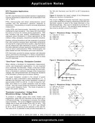
Figure 1 is a schematic diagram <strong>of</strong> a <strong>CdS</strong> cell <strong>and</strong> its<br />
operation circuit. An electrode is set at each end <strong>of</strong> the<br />
photoconductor. In darkness, the photoconductor<br />
resistance is very high. When a voltage is applied, the<br />
ammeter shows only a small dark current. This is the<br />
<strong>CdS</strong> photoconductor’s characteristic thermal equilibrium<br />
current. When light is incident on this photoconductor,<br />
a current I flows. Figure 2 shows the current that<br />
flows when the amount <strong>of</strong> light is increased.<br />
Figure 1: <strong>CdS</strong> Cell Schematic Diagram <strong>and</strong><br />
Operation Circuit<br />
Figure 2: Carrier Generation by Light Excitation<br />
Here are the basic principles <strong>of</strong> the photoconductive effect.<br />
(I) Directly beneath the conduction b<strong>and</strong> <strong>of</strong> the <strong>CdS</strong> crystal<br />
is a donor level <strong>and</strong> there is an acceptor level before the<br />
valence b<strong>and</strong>. In darkness, the electrons <strong>and</strong> holes in<br />
each level are almost crammed in place in the crystal<br />
<strong>and</strong> the photoconductor is at high resistance.<br />
(II) When light illuminates the <strong>CdS</strong> crystal <strong>and</strong> is absorbed<br />
by the crystal, the electrons in the valence b<strong>and</strong> are<br />
excited into the conduction b<strong>and</strong>. This creates pairs<br />
<strong>of</strong> free holes in the valence b<strong>and</strong> <strong>and</strong> free electrons<br />
in the conduction b<strong>and</strong>, increasing the conductance.<br />
(III)Furthermore, near the valence b<strong>and</strong> is a separate<br />
acceptor level that can capture free electrons only<br />
with difficulty, but captures free holes easily. This<br />
lowers the recombination probability <strong>of</strong> the electrons<br />
<strong>and</strong> holes, therefore increasing the number for electrons<br />
in the conduction b<strong>and</strong> for N-type conductance.<br />
The increase in conductance in (II) requires that the<br />
light energy be greater than the b<strong>and</strong> gap Eg. For Cds<br />
with a b<strong>and</strong> gap 2.41 eV, the absorption edge wavelength<br />
λ is λ = c/ν = hc/Eph = 1240/Eg ~ 515(nm).<br />
Where:<br />
Eph: photon energy (hν)<br />
h: Planck’s constant<br />
ν: light frequency<br />
c: speed <strong>of</strong> light<br />
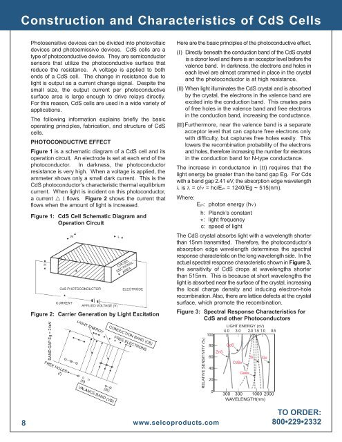
The <strong>CdS</strong> crystal absorbs light with a wavelength shorter<br />
than 15nm transmitted. Therefore, the photoconductor’s<br />
absorption edge wavelength determines the spectral<br />
response characteristic on the long wavelength side. In the<br />
actual spectral response characteristic shown in Figure 3,<br />
the sensitivity <strong>of</strong> <strong>CdS</strong> drops at wavelengths shorter<br />
than 515nm. This is because at short wavelengths the<br />
light is absorbed near the surface <strong>of</strong> the crystal, increasing<br />
the local charge density <strong>and</strong> inducing electron-hole<br />
recombination. Also, there are lattice defects at the crystal<br />
surface, which promote the recombination.<br />
Figure 3: Spectral Response <strong>Characteristics</strong> for<br />
<strong>CdS</strong> <strong>and</strong> other Photoconductors<br />
RELATIVE SENSITIVITY (%)<br />
100<br />
0<br />
LIGHT ENERGY (cV)<br />
4.0 3.0 2.0 1.5 1.0 0.5<br />
80 <strong>CdS</strong><br />
ZnS<br />
60<br />
Si<br />
<strong>CdS</strong>e<br />
40<br />
GaAs<br />
20<br />
Ge<br />
300 300 1000 2000<br />
WAVELENGTH(nm)<br />
8<br />
www.selcoproducts.com<br />
TO ORDER:<br />
800 229 2332
<strong>Construction</strong> <strong>and</strong> <strong>Characteristics</strong> <strong>of</strong> <strong>CdS</strong> <strong>Cells</strong><br />
Until the carries generated in (II) <strong>and</strong> (III) recombine,<br />
electrons are injected from one electrode <strong>and</strong> pulled<br />
out by the other.<br />
When these carries last longer <strong>and</strong> they move more,<br />
the conductance increases greatly. The conductance<br />
p is given by the following equation:<br />
p = ef (µ n τ n + µ p τ p)<br />
Where µn, µp: free electron, free hole movement (cm/V sec)<br />
τ n, τ n: free electron, free hole life (sec)<br />
f:number <strong>of</strong> generated carriers per second<br />
per cubic volume<br />
For a <strong>CdS</strong> cell, µ n τ n >> µ p τ p <strong>and</strong> conductance by<br />
free holes can be ignored. Then it becomes an N type<br />
semiconductor. Thus,<br />
p = ef µ n τ n<br />
Here, the gain G is defined as how many electrons flow<br />
between the electrodes due to excitation by one photon<br />
in the <strong>CdS</strong> photoconductor (until the carrier lifespan is over).<br />
These types are the sintered type, the single crystal<br />
type <strong>and</strong> the evaporated type. We use the sintered film<br />
fabrication method because it <strong>of</strong>fers high sensitivity<br />
areas, a large mass production effect <strong>and</strong> relatively<br />
superior production pr<strong>of</strong>itability.<br />
The process for making sintered <strong>CdS</strong> cell Impurities<br />
<strong>and</strong> a fusing agent for encouraging crystal growth are<br />
added to highly pure <strong>CdS</strong> crystal powder <strong>and</strong> this mixture<br />
is dissolved in water. The resulting solution is applied<br />
to <strong>CdS</strong> ceramic substrate <strong>and</strong> dried, then it is sintered<br />
in a high-temperature oven to form multiple crystals. In<br />
this way, a thick layer with the photoconductive effect<br />
is formed.<br />
Lead terminals are introduced to the <strong>CdS</strong> substrate<br />
<strong>and</strong> the <strong>CdS</strong> is packaged (Figure 4 <strong>and</strong> Photo 1<br />
shows an example <strong>of</strong> the structure <strong>of</strong> a plastic<br />
coated <strong>CdS</strong> cell).<br />
Figure 4: Structure <strong>of</strong> Plastic-Coated <strong>CdS</strong> Cell<br />
G = τ n/tt<br />
Where tt: transit time between electrodes = 12/V µ n<br />
l: distance between electrodes<br />
V: voltage applied<br />
Therefore,<br />
G = µ n τ nV/1 2<br />
For example, µ n = 300 cm2/V sec, τ n = 10-3 sec, 1<br />
= 0.2mm, <strong>and</strong> 1.2V, then the gain is 900. This means<br />
that there is multiplication in the <strong>CdS</strong> photoconductor<br />
<strong>and</strong> that the <strong>CdS</strong> is highly sensitive.<br />
The sensitivity <strong>of</strong> <strong>CdS</strong> is the change in resistance, i.e.,<br />
the change in current in response to change in light. As<br />
Figure 1 shows, if the distance between the electrodes is<br />
1 the cross-sectional area <strong>of</strong> the photoconductor is S,<br />
<strong>and</strong> the voltage applied is V, then from Ohm’s law:<br />
I 4 p S V/1 = p t V/1<br />
If the conductance p <strong>and</strong> the photoconductor<br />
thickness t are held constant, then:<br />
I 4 d/1 resistance R 4 1/d<br />
This 1/d is an important factor in designing the<br />
electrode configuration. In other words, the shorter the<br />
distance between the electrodes <strong>and</strong> the greater the<br />
electrode length, the higher the sensitivity <strong>and</strong> the<br />
lower the cell resistance. Thus, the electrode patterns<br />
for high-sensitivity <strong>CdS</strong> cells consist <strong>of</strong> many zig-zags.<br />
STRUCTURE<br />
<strong>CdS</strong> cells can be separated by the manufacturing<br />
process <strong>of</strong> the photoconductive layer into three types.<br />
Photo 1: Examples <strong>of</strong> <strong>CdS</strong> Cell Configurations<br />
TO ORDER:<br />
800 229 2332 www.selcoproducts.com<br />
9
<strong>Construction</strong> <strong>and</strong> <strong>Characteristics</strong> <strong>of</strong> <strong>CdS</strong> <strong>Cells</strong><br />
CHARACTERISTICS<br />
In the selection <strong>of</strong> a suitable <strong>CdS</strong> cell, the characteristics<br />
required by the functions <strong>of</strong> the circuit in which the <strong>CdS</strong><br />
cell is to be used are important. There are analog uses<br />
such as light measurement <strong>and</strong> digital uses such as<br />
on-<strong>of</strong>f switching. Use in digital circuits such as switching<br />
requires a fast response <strong>and</strong> a high ratio between<br />
illuminated resistance <strong>and</strong> dark resistance. The sensitivity<br />
<strong>of</strong> the slope <strong>of</strong> resistance vs. illuminance (gamma) <strong>and</strong><br />
the spectral response are important for measurement<br />
<strong>of</strong> brightness with devices such as illumination <strong>and</strong><br />
exposure meters. Therefore, underst<strong>and</strong>ing the various<br />
characteristics <strong>of</strong> <strong>CdS</strong> cell presented below is important<br />
for selecting the right <strong>CdS</strong> cell for your application.<br />
MAXIMUM RATINGS<br />
The maximum ratings given are absolute maximum<br />
ratings. This means that these are the values which<br />
are not to be exceeded even momentarily. Values<br />
above the maximum rating may break down the <strong>CdS</strong><br />
cell <strong>and</strong> lower it’s performance. Take adequate care in<br />
circuit design to avoid exceeding the maximum ratings.<br />
Allowable Power Dissipation<br />
Allowable power dissipation is the limiting value <strong>of</strong><br />
power consumption <strong>of</strong> a <strong>CdS</strong> cell when it is operated in<br />
a circuit. If a <strong>CdS</strong> cell is operated under conditions that<br />
cause the allowable power dissipation to be exceeded,<br />
deterioration <strong>of</strong> performance is hastened <strong>and</strong> the<br />
photoconductive surface can be damaged or broken<br />
down. This parameter must be held within the ratings<br />
in the same manner as are the applied voltage <strong>and</strong><br />
ambient temperature. Allowable power dissipation<br />
applies to total illumination <strong>of</strong> the photoconductive<br />
surface <strong>of</strong> a <strong>CdS</strong> cell. When only part <strong>of</strong> the surface is<br />
used, the allowable power dissipation must be reduced<br />
in proportion to the illuminated surface area.<br />
The allowable power dissipation figures in this catalog<br />
are for a temperature <strong>of</strong> 25°C. When these <strong>CdS</strong> cells<br />
are used at higher ambient temperature, the power<br />
consumption must be reduced, as the derating shown<br />
in Figure 5. This point must be taken into consideration<br />
as well.<br />
Ambient Temperature Range<br />
Unless otherwise specified, the maximum rated<br />
ambient temperature range is for <strong>CdS</strong> cell operation<br />
<strong>and</strong> storage. Operating or storing a <strong>CdS</strong> cell outside <strong>of</strong><br />
this temperature range reduces its performance.<br />
Never keep or operate <strong>CdS</strong> cells at temperature<br />
exceeding the maximum rating. It is suggested to keep<br />
<strong>CdS</strong> cells at a normal room temperature <strong>and</strong> humidity<br />
before using them.<br />
Figure 5: Allowable Power Dissipation vs. Ambient<br />
Temperature<br />
ALLOWABLE POWER DISSIPATION (%)<br />
100<br />
80<br />
60<br />
40<br />
20<br />
0<br />
-30 0 20 40 60 80 100<br />
AMBIENT TEMPERATURE (°C)<br />
Even within the ambient temperature range, the cell<br />
resistance, response, <strong>and</strong> other characteristics vary<br />
somewhat with the temperature, take this into<br />
consideration.<br />
Applied Voltage<br />
The maximum applied voltage is the voltage that can<br />
be applied between two terminals <strong>of</strong> a <strong>CdS</strong> cell. When<br />
the <strong>CdS</strong> cell resistance is at its maximum (the<br />
equilibrium dark resistance in total darkness), the<br />
voltage that can be applied between the <strong>CdS</strong> cell<br />
terminals is also at its maximum. Never let the applied<br />
voltage exceed the maximum rating. If the power<br />
consumption increases during <strong>CdS</strong> cell operation, the<br />
rating <strong>of</strong> allowable power dissipation should take<br />
precedence over the applied voltage rating.<br />
SENSITIVITY<br />
Spectral Response Characteristic<br />
The relative sensitivity <strong>of</strong> a <strong>CdS</strong> cell is dependent on<br />
the wavelength <strong>of</strong> the incident light. The sensitivity as<br />
a function <strong>of</strong> wavelength is called the spectral<br />
response characteristic. Fundamentally, the maximum<br />
sensitivity wavelength (or peak wavelength) for <strong>CdS</strong><br />
cell is 515nm. By controlling the composition ratio <strong>of</strong><br />
<strong>CdS</strong> to <strong>CdS</strong>e, the maximum sensitivity can be<br />
optimized at a wavelength between 515 <strong>and</strong> 730nm.<br />
Photoconductive cells with spectral response close to<br />
that <strong>of</strong> the human eye are available.<br />
10<br />
www.selcoproducts.com<br />
TO ORDER:<br />
800 229 2332
<strong>Construction</strong> <strong>and</strong> <strong>Characteristics</strong> <strong>of</strong> <strong>CdS</strong> <strong>Cells</strong><br />
Figure 6 shows these relationships. <strong>CdS</strong>, Cd (S.Se),<br />
<strong>and</strong> <strong>CdS</strong>e cells are <strong>of</strong>ten called “<strong>CdS</strong> cells”.<br />
By using a <strong>CdS</strong> cell with a spectral response similar to<br />
the human eye, it can be widely <strong>and</strong> easily be used in<br />
applications as sensors substituting for the human eye.<br />
Figure 6: Spectral Response <strong>of</strong> <strong>CdS</strong> <strong>Cells</strong> <strong>and</strong> Spectral<br />
Luminous Efficiency (Human Eye Response)<br />
luminous intensity I (cd) is obtained from the equation:<br />
E (lux) =<br />
This is based on the st<strong>and</strong>ard luminous efficiency, so<br />
these are light measurement units for the visible region<br />
only.<br />
I<br />
D 2<br />
RELATIVE SENSITIVITY (%)<br />
100<br />
80<br />
60<br />
40<br />
20<br />
LUMINOUS<br />
EFFICIENCY<br />
<strong>CdS</strong><br />
<strong>CdS</strong>e<br />
Cd (S.Se)<br />
Table 1: Illuminance Conversion Table<br />
Conversion value<br />
Foot-Cadle<br />
(Ft-C)<br />
Foot-cadle<br />
(Ft-C)<br />
Lux<br />
Photo<br />
1 0.0929 929<br />
Lux = 1m/m 2 10.76 1 10.000<br />
Photo 0.00108 0.0001 1<br />
0<br />
400 500 600 700 800 900 1000<br />
WAVELENGTH (nm)<br />
<strong>CdS</strong>: cadmium sulfide<br />
Cd(S.Se): cadmium sulfo-selenium<br />
<strong>CdS</strong>e: cadmium selenide<br />
Expressing Sensitivity<br />
The sensitivity <strong>of</strong> light sensors expresses the relation<br />
between the intensity <strong>of</strong> the light impinging on the<br />
sensitive surface <strong>and</strong> the resulting output signal. If<br />
voltage V is applied across a <strong>CdS</strong> cell <strong>and</strong> illuminance<br />
E (lux) is shown on it, <strong>and</strong> signal current IL flow, then:<br />
I L = K V α E m<br />
Where K is a constant, α is the voltage index for signal<br />
current <strong>and</strong> can be treated as just about 1. m (gamma)<br />
is also called the illuminance index for signal current<br />
<strong>and</strong> shows the slope <strong>of</strong> the signal current vs. illuminance<br />
characteristic.<br />
As the above equation shows, the sensitivity can be<br />
expressed as the value <strong>of</strong> the signal current with<br />
respect to the incident illuminance, but usually, rather<br />
than expressed in the signal current, the sensitivity is<br />
expressed in the cell resistance.<br />
REFERENCE<br />
Lux is unit <strong>of</strong> illuminance, equal to the illuminance on a<br />
surface 1 square meter in area on which there is a<br />
luminous flux <strong>of</strong> 1 lumen uniformly distributed. The<br />
illuminance is proportional to the square <strong>of</strong> the<br />
distance from the light source. The illuminance E (lux)<br />
at a distance D meters from a point light source <strong>of</strong><br />
1 foot-0c<strong>and</strong>le<br />
E = I/D 2 =1cd/0.3048 2 = 10.764 (lux)<br />
(1 foot = 0.3048 meter)<br />
The lux is a light measurement unit based on the st<strong>and</strong>ard<br />
luminous efficiency. Light sensors with spectral response<br />
characteristics which are shifted from the st<strong>and</strong>ard luminous<br />
efficiency show different output signals if the radiant<br />
spectral distribution (color temperature) <strong>of</strong> the light source<br />
is different, even if the illuminance is the same. Therefore,<br />
when using light sources for light measurement, the radiant<br />
spectral distribution characteristic must be specified.<br />
A tungsten lamp with a color temperature <strong>of</strong> 2856K is<br />
used as the st<strong>and</strong>ard light source. The color temperature<br />
<strong>of</strong> the tungsten lamp is expressed as the absolute<br />
temperature <strong>of</strong> a black body (a platinum black body<br />
furnace). This color temperature is approximately<br />
proportional in the visible region to the spectral radiant<br />
distribution <strong>of</strong> the lamp.<br />
Figure 7: Spectral Energy Distribution for 2856K<br />
Black Body<br />
RELATIVE SENSITIVITY (%)<br />
100<br />
80<br />
60<br />
40<br />
20<br />
0<br />
300 400 500 600 700 800 900 1000 1100 1200 1300<br />
WAVELENGTH (nm)<br />
TO ORDER:<br />
800 229 2332 www.selcoproducts.com<br />
11
<strong>Construction</strong> <strong>and</strong> <strong>Characteristics</strong> <strong>of</strong> <strong>CdS</strong> <strong>Cells</strong><br />
ILLUMINANCE VS. RESISTANCE<br />
Figure 8 gives a typical example <strong>of</strong> graphing the <strong>CdS</strong><br />
cell resistance as a function <strong>of</strong> incident illuminance.<br />
The slope <strong>of</strong> this curve, m (gamma), varies with the cell<br />
type <strong>and</strong> is important for detecting analog-like light<br />
level differences. This is given by the tangent θ <strong>of</strong> a<br />
line connecting two points on the curve. If the illuminated<br />
resistances at illuminance Ea (lux) <strong>and</strong> Ed (lux) are Ra<br />
(Ω) <strong>and</strong> Rb (Ω), then m between a <strong>and</strong> b is expressed<br />
by the following equation:<br />
m a b = tanθ = I logIa - logIb<br />
E<br />
= logEa - logEb = log(Ia/Ib)<br />
log(Ea/Eb)<br />
(Ia. Ib...the signal current when the <strong>CdS</strong> is illuminated)<br />
= R logRa - logRb<br />
E<br />
= logEa - logEb = log(Ra/Rb)<br />
log(Ea/Eb)<br />
SIGNAL CURRENT VS. APPLIED VOLTAGE<br />
Figure 9 shows the signal current vs. applied voltage<br />
characteristic for different illuminance levels. This<br />
characteristic is nearly linear <strong>and</strong> holds for applied<br />
voltages down to 1V <strong>and</strong> consumption near the<br />
allowable power dissipation. The amount <strong>of</strong> heat<br />
generated by the <strong>CdS</strong> cell increases, causing a<br />
change in cell resistance. Linearity becomes lost,<br />
therefore take precautions in system designs.<br />
Figure 9: Signal Current vs. Applied Voltage<br />
Characteristic Example<br />
100<br />
10<br />
LIGHT SOURCE - 2856K<br />
Ta = 25°C<br />
Usually, m is expressed as m 100 /10, the slope between the<br />
100 lux <strong>and</strong> 10 lux. So the above equation becomes:<br />
m 100/ 10 =<br />
log(Ra/Rb)<br />
log(Ea/Eb) = log(R100/R10)<br />
log(100/10)<br />
= log(R100/R10)<br />
From this relationship, the conversion equation is obtained<br />
Ra = Rbx (Ea/Eb) - m a b<br />
If the slope m a b<br />
<strong>and</strong> the illuminated resistance Rb are<br />
known, the illuminated resistance for any point<br />
between Ea <strong>and</strong> Eb can be obtained. This relationship<br />
gives the equation:<br />
Ea = Eb x (Ra/Rb) 1/m a b<br />
Given the value <strong>of</strong> m a b<br />
<strong>and</strong> the illuminated resistance<br />
Rb at illuminance Eb, the illuminance Ea that will give<br />
a illuminated resistance <strong>of</strong> Ra can be obtained.<br />
Figure 8: <strong>CdS</strong> Resistance vs. Illuminance Characteristic<br />
Example<br />
CELL RESISTANCE (kΩ)<br />
10000<br />
1000<br />
100<br />
10<br />
Rb<br />
Ra<br />
LIGHT SOURCE - 2856K<br />
Ta: 25°C<br />
1<br />
Eb<br />
Ea<br />
0.1 1 10 100 1000<br />
ILLUMINANCE (ι x)<br />
SIGNAL CURRENT (mA)<br />
1<br />
0.1<br />
1000 ι x<br />
100 ι x<br />
10 ι x<br />
ALLOWABLE POWER DISSIPATION: 70mW<br />
1 ι x<br />
0.1 ι x<br />
0.01<br />
1 10 100 1000<br />
APPLIED VOLTAGE (Vdc)<br />
DARK RESISTANCE/DARK CURRENT<br />
If a <strong>CdS</strong> cell is left in total darkness for 15 hours <strong>and</strong> the<br />
resistance is measured, the resistance value will be high.<br />
This is true dark resistance (equilibrium dark resistance).<br />
In practical applications, the <strong>CdS</strong> cell is used at various<br />
light levels. The previous light levels affect the dark<br />
resistance, which is called light history effect. Therefore,<br />
the dark resistance must be expressed specifying the<br />
time allowed after the incident light is removed. In this<br />
catalog, the dark resistance is measured 10 seconds<br />
after incident light <strong>of</strong> 10 lux has been cut <strong>of</strong>f. This dark<br />
resistance measurement can also be viewed as expressing<br />
the response time (fall time) for <strong>CdS</strong> cells.<br />
RESPONSE SPEED<br />
<strong>CdS</strong> cells have a certain time delay in responding to<br />
incident light. This response speed is an important<br />
point in designing detection <strong>of</strong> rapidly changing light<br />
levels <strong>and</strong> on-<strong>of</strong>f switches.<br />
The response speed is usually expressed as the time<br />
required for the illuminated resistance to reach 63% <strong>of</strong> its<br />
saturation value after the cell is illuminated (rise time),<br />
12<br />
www.selcoproducts.com<br />
TO ORDER:<br />
800 229 2332
<strong>Construction</strong> <strong>and</strong> <strong>Characteristics</strong> <strong>of</strong> <strong>CdS</strong> <strong>Cells</strong><br />
<strong>and</strong> as the time required for the illuminated resistance<br />
to fall to 37% <strong>of</strong> its saturation value after the light is<br />
removed (fall time). The rise <strong>and</strong> fall times listed in this<br />
catalog are measured with repetitive intermittent light.<br />
Figure 10: Rise Time <strong>and</strong> Fall Time<br />
100%<br />
0 ι x<br />
10 ι x<br />
1 ι x<br />
<strong>CdS</strong> CELL<br />
Vout<br />
R ι < 1 /100 x ILLUMINATED RESISTANCE<br />
63%<br />
tr10<br />
td10<br />
tr1<br />
td1<br />
tr10, tr1: Rise Times at 10 ι x <strong>and</strong> 1 ι x<br />
td10, t1: Fall Times at 10 ι x <strong>and</strong> 1 ι x<br />
37%<br />
The response speed varies considerably with the light<br />
level, the light history condition, the lad resistance, the<br />
ambient temperature, <strong>and</strong> other factors. The higher<br />
the incident light level, the faster the response speed.<br />
Also, cells kept in darkness exhibit slower response<br />
than cells kept at a brighter light level. This effect<br />
becomes more distinct as the cell is kept for longer<br />
periods at a dark light level. Also, the apparent rise<br />
time becomes faster with a larger load resistance, but<br />
the fall time shows the contrary effect.<br />
LIGHT HISTORY EFFECT<br />
As described before, the illuminated resistance, dark<br />
resistance, <strong>and</strong> response speed vary with the conditions<br />
to which the <strong>CdS</strong> cell has previously been exposed.<br />
This is called the light history effect. In particular, if the<br />
<strong>CdS</strong> cell has been kept in darkness or brightness prior<br />
to measurement, this results in a difference in illuminated<br />
resistance (i.e. sensitivity). This difference is called the<br />
light history error. In general, when a cell is kept in<br />
darkness for a long time, its illuminated resistance will<br />
be lower compared to a cell kept at a light level. This<br />
light history error indicates the initial change in the<br />
illuminated resistance from the previous condition <strong>of</strong><br />
the saturation (recovery) region. This is different from<br />
the change in resistance when the <strong>CdS</strong> cell is kept in<br />
operation with the saturated illuminated resistance or<br />
‘drift’.<br />
Under the conditions given in Figure 11, some cells<br />
may show light history errors as large as 50%. This is<br />
<strong>of</strong>ten seen in <strong>CdS</strong>e cells with a maximum sensitivity<br />
wavelength at near 730nm.<br />
Figure 11: Light History Effect Example<br />
CELL RESISTANCE 1ιx (kΩ)<br />
260<br />
240<br />
220<br />
200<br />
180<br />
160<br />
Ta = 25°C<br />
LIGHT SOURCE = 2856K<br />
AFTER ILLUMINATED WITH 1000/ιx<br />
AFTER BEING KEPT IN<br />
DARKNESS FOR 48 HOURS<br />
140<br />
0 20 40 60 80 100 120 140 160<br />
DURATION OF MEASUREMENT OF 1 lux (seconds)<br />
Because <strong>CdS</strong> cells have this light history effect, particularly<br />
when they are used at low illuminance levels (1 lux or<br />
less as a general guide), this phenomenon must be<br />
considered. In some cases, in order to reduce the light<br />
history effect, the <strong>CdS</strong> cell can be used after being<br />
exposed to light for several minutes. All the values listed<br />
in this catalog have been measured with the cell left<br />
exposed to 100 to 500 lux for 1 to 2 hours before<br />
measurement.<br />
TEMPERATURE CHARACTERISTICS<br />
The change in the cell resistance with ambient temperature<br />
depends on the light level. In general, the lower the<br />
illuminance, the greater the change in resistance with<br />
temperature change. Also, the slope <strong>of</strong> the temperature<br />
coefficient (positive or negative) depends on the<br />
composition <strong>and</strong> the fabrication method <strong>of</strong> the <strong>CdS</strong> cell.<br />
Figure 12: Temperature Characteristic Examples<br />
CHANGE IN ILLUMINATED RESISTANCE (%)<br />
130<br />
120<br />
110<br />
100<br />
90<br />
80<br />
LIGHT SOURCE = 2856K<br />
1ι x<br />
10ι x<br />
100ι x<br />
70<br />
-40 -20 0 +20 +40 +60 +80<br />
AMBIENT TEMPERATURE (°C)<br />
TO ORDER:<br />
800 229 2332 www.selcoproducts.com<br />
13
<strong>Construction</strong> <strong>and</strong> <strong>Characteristics</strong> <strong>of</strong> <strong>CdS</strong> <strong>Cells</strong><br />
OPERATING LIFE<br />
Figure 13 illustrates the change in illuminated resistance<br />
(at 10 lux) <strong>of</strong> <strong>CdS</strong> cells with operating time, showing<br />
slightly increasing curves. If used within the maximum<br />
ratings specified in this catalog, the <strong>CdS</strong> cell recovers<br />
from this time change <strong>and</strong> maintains stable values for<br />
quite a long period. Exceeding the maximum ratings<br />
can cause deterioration or damage. If this is kept in<br />
mind, the life <strong>of</strong> <strong>CdS</strong> cells can be expected to be quite<br />
long.<br />
Figure 13: Change In Illuminated Resistance vs.<br />
Operating Time<br />
RESISTANCE AT 10 ι x (%)<br />
140<br />
120<br />
100<br />
80<br />
Ta = 80°C<br />
CONTINUOS<br />
STORAGE AT 100ιx<br />
Ta = 60°C<br />
CONTINUOS<br />
OPERATION AT 20mW<br />
60<br />
1 10 100 1000<br />
TIME (h)<br />
14<br />
www.selcoproducts.com<br />
TO ORDER:<br />
800 229 2332