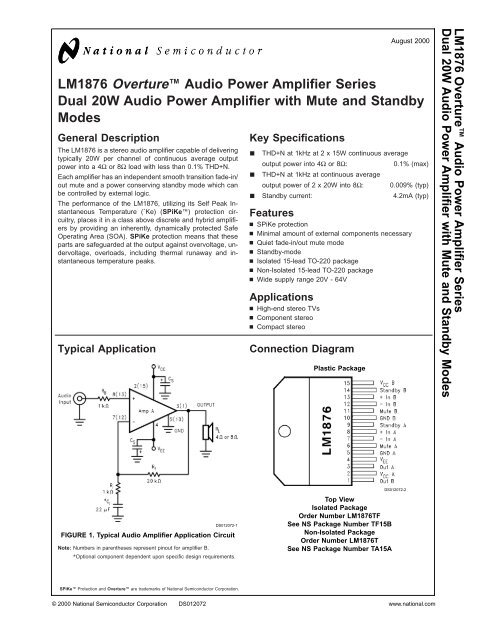
LM1876 Overture Audio Power Amplifier Series Dual 20W Audio ...
LM1876 Overture Audio Power Amplifier Series Dual 20W Audio ...
LM1876 Overture Audio Power Amplifier Series Dual 20W Audio ...

Create successful ePaper yourself
Turn your PDF publications into a flip-book with our unique Google optimized e-Paper software.
<strong>LM1876</strong> <strong>Overture</strong> <strong>Audio</strong> <strong>Power</strong> <strong>Amplifier</strong> <strong>Series</strong><br />
<strong>Dual</strong> <strong>20W</strong> <strong>Audio</strong> <strong>Power</strong> <strong>Amplifier</strong> with Mute and Standby<br />
Modes<br />
General Description<br />
The <strong>LM1876</strong> is a stereo audio amplifier capable of delivering<br />
typically <strong>20W</strong> per channel of continuous average output<br />
power into a 4Ω or 8Ω load with less than 0.1% THD+N.<br />
Each amplifier has an independent smooth transition fade-in/<br />
out mute and a power conserving standby mode which can<br />
be controlled by external logic.<br />
The performance of the <strong>LM1876</strong>, utilizing its Self Peak Instantaneous<br />
Temperature (˚Ke) (SPiKe) protection circuitry,<br />
places it in a class above discrete and hybrid amplifiers<br />
by providing an inherently, dynamically protected Safe<br />
Operating Area (SOA). SPiKe protection means that these<br />
parts are safeguarded at the output against overvoltage, undervoltage,<br />
overloads, including thermal runaway and instantaneous<br />
temperature peaks.<br />
Typical Application<br />
Key Specifications<br />
j<br />
j<br />
THD+N at 1kHz at 2 x 15W continuous average<br />
output power into 4Ω or 8Ω:<br />
0.1% (max)<br />
THD+N at 1kHz at continuous average<br />
output power of 2 x <strong>20W</strong> into 8Ω:<br />
0.009% (typ)<br />
j Standby current: 4.2mA (typ)<br />
Features<br />
n SPiKe protection<br />
n Minimal amount of external components necessary<br />
n Quiet fade-in/out mute mode<br />
n Standby-mode<br />
n Isolated 15-lead TO-220 package<br />
n Non-Isolated 15-lead TO-220 package<br />
n Wide supply range 20V - 64V<br />
Applications<br />
n High-end stereo TVs<br />
n Component stereo<br />
n Compact stereo<br />
Connection Diagram<br />
Plastic Package<br />
August 2000<br />
<strong>LM1876</strong> <strong>Overture</strong> <strong>Audio</strong> <strong>Power</strong> <strong>Amplifier</strong> <strong>Series</strong><br />
<strong>Dual</strong> <strong>20W</strong> <strong>Audio</strong> <strong>Power</strong> <strong>Amplifier</strong> with Mute and Standby Modes<br />
DS012072-1<br />
FIGURE 1. Typical <strong>Audio</strong> <strong>Amplifier</strong> Application Circuit<br />
Note: Numbers in parentheses represent pinout for amplifier B.<br />
*Optional component dependent upon specific design requirements.<br />
Top View<br />
Isolated Package<br />
Order Number <strong>LM1876</strong>TF<br />
See NS Package Number TF15B<br />
Non-Isolated Package<br />
Order Number <strong>LM1876</strong>T<br />
See NS Package Number TA15A<br />
DS012072-2<br />
SPiKe Protection and <strong>Overture</strong> are trademarks of National Semiconductor Corporation.<br />
© 2000 National Semiconductor Corporation DS012072 www.national.com
<strong>LM1876</strong><br />
Absolute Maximum Ratings (Notes 4, 5)<br />
If Military/Aerospace specified devices are required,<br />
please contact the National Semiconductor Sales Office/<br />
Distributors for availability and specifications.<br />
Supply Voltage |V CC |+|V EE |<br />
(No Input)<br />
Supply Voltage |V CC |+|V EE |<br />
(with Input)<br />
Common Mode Input Voltage<br />
Differential Input Voltage<br />
Output Current<br />
64V<br />
64V<br />
(V CC or V EE ) and<br />
|V CC |+|V EE | ≤ 54V<br />
54V<br />
Internally Limited<br />
<strong>Power</strong> Dissipation (Note 6) 62.5W<br />
ESD Susceptability (Note 7)<br />
2000V<br />
Junction Temperature (Note 8)<br />
150˚C<br />
Thermal Resistance<br />
Isolated TF-Package<br />
θ JC<br />
Non-Isolated T-Package<br />
θ JC<br />
Soldering Information<br />
TF Package (10 sec.)<br />
Storage Temperature<br />
Operating Ratings (Notes 4, 5)<br />
Temperature Range<br />
T MIN ≤ T A ≤ T MAX<br />
Supply Voltage |V CC |+|V EE | (Note 1)<br />
2˚C/W<br />
1˚C/W<br />
260˚C<br />
−40˚C to +150˚C<br />
−20˚C ≤ T A ≤ +85˚C<br />
20V to 64V<br />
Electrical Characteristics (Notes 4, 5)<br />
The following specifications apply for V CC = +22V, V EE = −22V with R L =8Ωunless otherwise specified. Limits apply for T A =<br />
25˚C.<br />
Symbol Parameter Conditions <strong>LM1876</strong> Units<br />
Typical Limit<br />
(Limits)<br />
(Note 9) (Note 10)<br />
|V CC | + <strong>Power</strong> Supply Voltage GND − V EE ≥ 9V 20 V (min)<br />
|V EE | (Note 11) 64 V (max)<br />
P O Output <strong>Power</strong> THD + N = 0.1% (max),<br />
(Note 3) (Continuous Average) f = 1 kHz<br />
|V CC |=|V EE | = 22V, R L =8Ω 20 15 W/ch (min)<br />
|V CC |=|V EE | = 20V, R L =4Ω(Note 13) 22 15 W/ch (min)<br />
THD + N Total Harmonic Distortion 15 W/ch, R L =8Ω 0.08 %<br />
Plus Noise 15 W/ch, R L =4Ω,|V CC |=|V EE | = 20V 0.1 %<br />
20 Hz ≤ f ≤ 20 kHz, A V =26dB<br />
X talk Channel Separation f = 1 kHz, V O = 10.9 Vrms 80 dB<br />
SR Slew Rate V IN = 1.414 Vrms, t rise = 2 ns 18 12 V/µs (min)<br />
(Note 3)<br />
I total Total Quiescent <strong>Power</strong> Both <strong>Amplifier</strong>s V CM = 0V,<br />
(Note 2) Supply Current V O = 0V, I O =0mA<br />
Standby: Off 50 80 mA (max)<br />
Standby: On 4.2 6 mA (max)<br />
V OS Input Offset Voltage V CM = 0V, I O = 0 mA 2.0 15 mV (max)<br />
(Note 2)<br />
I B Input Bias Current V CM = 0V, I O = 0 mA 0.2 0.5 µA (max)<br />
I OS Input Offset Current V CM = 0V, I O = 0 mA 0.002 0.2 µA (max)<br />
I O Output Current Limit |V CC |=|V EE | = 10V, t ON = 10 ms, 3.5 2.9 Apk (min)<br />
V O =0V<br />
V OD Output Dropout Voltage |V CC –V O |, V CC = 20V, I O = +100 mA 1.8 2.3 V (max)<br />
(Note 2) (Note 12) |V O –V EE |, V EE = −20V, I O = −100 mA 2.5 3.2 V (max)<br />
PSRR <strong>Power</strong> Supply Rejection Ratio V CC = 25V to 10V, V EE = −25V, 115 85 dB (min)<br />
(Note 2)<br />
V CM = 0V, I O =0mA<br />
V CC = 25V, V EE = −25V to −10V 110 85 dB (min)<br />
V CM = 0V, I O =0mA<br />
CMRR Common Mode Rejection Ratio V CC = 35V to 10V, V EE = −10V to −35V, 110 80 dB (min)<br />
(Note 2)<br />
V CM = 10V to −10V, I O =0mA<br />
www.national.com 2
Electrical Characteristics (Notes 4, 5) (Continued)<br />
The following specifications apply for V CC = +22V, V EE = −22V with R L =8Ωunless otherwise specified. Limits apply for T A =<br />
25˚C.<br />
Symbol Parameter Conditions <strong>LM1876</strong> Units<br />
Typical Limit<br />
(Limits)<br />
(Note 9) (Note 10)<br />
A VOL Open Loop Voltage Gain R L =2kΩ,∆V O = 20 V 110 90 dB (min)<br />
(Note 2)<br />
GBWP Gain Bandwidth Product f O = 100 kHz, V IN = 50 mVrms 7.5 5 MHz (min)<br />
e IN Input Noise IHF — A Weighting Filter 2.0 8 µV (max)<br />
(Note 3)<br />
R IN = 600Ω (Input Referred)<br />
SNR Signal-to-Noise Ratio P O = 1W, A — Weighted, 98 dB<br />
Measured at 1 kHz, R S =25Ω<br />
P O = 15W, A — Weighted 108 dB<br />
Measured at 1 kHz, R S =25Ω<br />
A M Mute Attenuation Pin 6,11 at 2.5V 115 80 dB (min)<br />
Standby<br />
Pin<br />
V IL Standby Low Input Voltage Not in Standby Mode 0.8 V (max)<br />
V IH Standby High Input Voltage In Standby Mode 2.0 2.5 V (min)<br />
Mute pin<br />
V IL Mute Low Input Voltage Outputs Not Muted 0.8 V (max)<br />
V IH Mute High Input Voltage Outputs Muted 2.0 2.5 V (min)<br />
Note 1: Operation is guaranteed up to 64V, however, distortion may be introduced from SPiKe Protection Circuitry if proper thermal considerations are not taken into<br />
account. Refer to the Application Information section for a complete explanation.<br />
Note 2: DC Electrical Test; Refer to Test Circuit #1.<br />
Note 3: AC Electrical Test; Refer to Test Circuit #2.<br />
Note 4: All voltages are measured with respect to the GND pins (5, 10), unless otherwise specified.<br />
Note 5: Absolute Maximum Ratings indicate limits beyond which damage to the device may occur. Operating Ratings indicate conditions for which the device is functional,<br />
but do not guarantee specific performance limits. Electrical Characteristics state DC and AC electrical specifications under particular test conditions which guarantee<br />
specific performance limits. This assumes that the device is within the Operating Ratings. Specifications are not guaranteed for parameters where no limit is<br />
given, however, the typical value is a good indication of device performance.<br />
Note 6: For operating at case temperatures above 25˚C, the device must be derated based on a 150˚C maximum junction temperature and a thermal resistance of<br />
θ JC = 2˚C/W (junction to case) for the TF package and θ JC = 1˚C/W for the T package. Refer to the section Determining the Correct Heat Sink in the Application Information<br />
section.<br />
Note 7: Human body model, 100 pF discharged through a 1.5 kΩ resistor.<br />
Note 8: The operating junction temperature maximum is 150˚C, however, the instantaneous Safe Operating Area temperature is 250˚C.<br />
Note 9: Typicals are measured at 25˚C and represent the parametric norm.<br />
Note 10: Limits are guarantees that all parts are tested in production to meet the stated values.<br />
Note 11: V EE must have at least −9V at its pin with reference to ground in order for the under-voltage protection circuitry to be disabled. In addition, the voltage differential<br />
between V CC and V EE must be greater than 14V.<br />
Note 12: The output dropout voltage, V OD , is the supply voltage minus the clipping voltage. Refer to the Clipping Voltage vs. Supply Voltage graph in the Typical Performance<br />
Characteristics section.<br />
Note 13: Fora4Ωload, and with ±20V supplies, the <strong>LM1876</strong> can deliver typically 22W of continuous average output power with less than 0.1% (THD + N). With<br />
supplies above ±20V, the <strong>LM1876</strong> cannot deliver more than 22W into a 4Ω due to current limiting of the output transistors. Thus, increasing the power supply above<br />
±20V will only increase the internal power dissipation, not the possible output power. Increased power dissipation will require a larger heat sink as explained in the<br />
Application Information section.<br />
<strong>LM1876</strong><br />
3<br />
www.national.com
<strong>LM1876</strong><br />
Test Circuit #1 (Note 2) (DC Electrical Test Circuit)<br />
DS012072-3<br />
Test Circuit #2 (Note 3) (AC Electrical Test Circuit)<br />
DS012072-4<br />
www.national.com 4
Bridged <strong>Amplifier</strong> Application Circuit<br />
<strong>LM1876</strong><br />
Single Supply Application Circuit<br />
FIGURE 2. Bridged <strong>Amplifier</strong> Application Circuit<br />
DS012072-5<br />
FIGURE 3. Single Supply <strong>Amplifier</strong> Application Circuit<br />
DS012072-6<br />
Note: *Optional components dependent upon specific design requirements.<br />
5<br />
www.national.com
<strong>LM1876</strong><br />
Auxiliary <strong>Amplifier</strong> Application Circuit<br />
FIGURE 4. Special <strong>Audio</strong> <strong>Amplifier</strong> Application Circuit<br />
DS012072-7<br />
Equivalent Schematic (excluding active protection circuitry)<br />
<strong>LM1876</strong> (per Amp)<br />
DS012072-8<br />
www.national.com 6
External Components Description<br />
Components<br />
Functional Description<br />
1 R B Prevents currents from entering the amplifier’s non-inverting input which may be passed through to the<br />
load upon power down of the system due to the low input impedance of the circuitry when the<br />
undervoltage circuitry is off. This phenomenon occurs when the supply voltages are below 1.5V.<br />
2 R i Inverting input resistance to provide AC gain in conjunction with R f .<br />
3 R f Feedback resistance to provide AC gain in conjunction with R i .<br />
4 C i<br />
(Note 14)<br />
Feedback capacitor which ensures unity gain at DC. Also creates a highpass filter with R i at f C =<br />
1/(2πR i C i ).<br />
5 C S Provides power supply filtering and bypassing. Refer to the Supply Bypassing application section for<br />
proper placement and selection of bypass capacitors.<br />
6 R V<br />
(Note 14)<br />
Acts as a volume control by setting the input voltage level.<br />
7 R IN<br />
(Note 14)<br />
8 C IN<br />
(Note 14)<br />
9 R SN<br />
(Note 14)<br />
10 C SN<br />
(Note 14)<br />
Sets the amplifier’s input terminals DC bias point when C IN is present in the circuit. Also works with C IN to<br />
create a highpass filter at f C = 1/(2πR IN C IN ). Refer to Figure 4.<br />
Input capacitor which blocks the input signal’s DC offsets from being passed onto the amplifier’s inputs.<br />
Works with C SN to stabilize the output stage by creating a pole that reduces high frequency instabilities.<br />
Works with R SN to stabilize the output stage by creating a pole that reduces high frequency instabilities.<br />
The pole is set at f C = 1/(2πR SN C SN ). Refer to Figure 4.<br />
11 L (Note 14) Provides high impedance at high frequencies so that R may decouple a highly capacitive load and reduce<br />
12 R (Note 14)<br />
the Q of the series resonant circuit. Also provides a low impedance at low frequencies to short out R and<br />
pass audio signals to the load. Refer to Figure 4.<br />
13 R A Provides DC voltage biasing for the transistor Q1 in single supply operation.<br />
14 C A Provides bias filtering for single supply operation.<br />
15 R INP<br />
(Note 14)<br />
Limits the voltage difference between the amplifier’s inputs for single supply operation. Refer to the Clicks<br />
and Pops application section for a more detailed explanation of the function of R INP .<br />
16 R BI Provides input bias current for single supply operation. Refer to the Clicks and Pops application section<br />
for a more detailed explanation of the function of R BI .<br />
17 R E Establishes a fixed DC current for the transistor Q1 in single supply operation. This resistor stabilizes the<br />
half-supply point along with C A .<br />
Note 14: Optional components dependent upon specific design requirements.<br />
<strong>LM1876</strong><br />
Typical Performance Characteristics<br />
THD+NvsFrequency<br />
THD+NvsFrequency<br />
THD+NvsFrequency<br />
DS012072-13<br />
DS012072-14<br />
DS012072-15<br />
7<br />
www.national.com
<strong>LM1876</strong><br />
Typical Performance Characteristics (Continued)<br />
THD+Nvs<br />
Output <strong>Power</strong><br />
THD+Nvs<br />
Output <strong>Power</strong><br />
THD+Nvs<br />
Output <strong>Power</strong><br />
DS012072-16<br />
DS012072-17<br />
DS012072-18<br />
THD+Nvs<br />
Output <strong>Power</strong><br />
THD+Nvs<br />
Output <strong>Power</strong><br />
THD+Nvs<br />
Output <strong>Power</strong><br />
DS012072-19<br />
DS012072-20<br />
DS012072-21<br />
Clipping Voltage vs<br />
Supply Voltage<br />
Clipping Voltage vs<br />
Supply Voltage<br />
Clipping Voltage vs<br />
Supply Voltage<br />
DS012072-22<br />
DS012072-23<br />
DS012072-24<br />
www.national.com 8
Typical Performance Characteristics (Continued)<br />
Output <strong>Power</strong> vs<br />
Load Resistance<br />
<strong>Power</strong> Dissipation vs<br />
Output <strong>Power</strong><br />
<strong>Power</strong> Dissipation vs<br />
Output <strong>Power</strong><br />
<strong>LM1876</strong><br />
DS012072-25<br />
DS012072-26<br />
DS012072-27<br />
Output <strong>Power</strong> vs<br />
Supply Voltage<br />
Output Mute vs<br />
Mute Pin Voltage<br />
Output Mute vs<br />
Mute Pin Voltage<br />
DS012072-28<br />
DS012072-29<br />
DS012072-30<br />
Channel Separation vs<br />
Frequency<br />
Pulse Response<br />
Large Signal Response<br />
DS012072-31<br />
DS012072-32<br />
DS012072-33<br />
9<br />
www.national.com
<strong>LM1876</strong><br />
Typical Performance Characteristics (Continued)<br />
<strong>Power</strong> Supply<br />
Rejection Ratio<br />
Common-Mode<br />
Rejection Ratio<br />
Open Loop<br />
Frequency Response<br />
DS012072-34<br />
DS012072-35<br />
DS012072-36<br />
Safe Area<br />
SPiKe Protection<br />
Response<br />
Supply Current vs<br />
Supply Voltage<br />
DS012072-37<br />
DS012072-38<br />
DS012072-39<br />
Pulse Thermal<br />
Resistance<br />
Pulse Thermal<br />
Resistance<br />
Supply Current vs<br />
Output Voltage<br />
DS012072-40<br />
DS012072-41<br />
DS012072-42<br />
www.national.com 10
Typical Performance Characteristics (Continued)<br />
Pulse <strong>Power</strong> Limit<br />
Pulse <strong>Power</strong> Limit<br />
Supply Current vs<br />
Case Temperature<br />
<strong>LM1876</strong><br />
DS012072-43<br />
DS012072-44<br />
DS012072-45<br />
Supply Current (I CC )vs<br />
Standby Pin Voltage<br />
Supply Current (I EE )vs<br />
Standby Pin Voltage<br />
Input Bias Current vs<br />
Case Temperature<br />
DS012072-46<br />
DS012072-47<br />
DS012072-48<br />
11<br />
www.national.com
<strong>LM1876</strong><br />
Application Information<br />
MUTE MODE<br />
By placing a logic-high voltage on the mute pins, the signal<br />
going into the amplifiers will be muted. If the mute pins are<br />
left floating or connected to a logic-low voltage, the amplifiers<br />
will be in a non-muted state. There are two mute pins,<br />
one for each amplifier, so that one channel can be muted<br />
without muting the other if the application requires such a<br />
configuration. Refer to the Typical Performance Characteristics<br />
section for curves concerning Mute Attenuation vs<br />
Mute Pin Voltage.<br />
STANDBY MODE<br />
The standby mode of the <strong>LM1876</strong> allows the user to drastically<br />
reduce power consumption when the amplifiers are<br />
idle. By placing a logic-high voltage on the standby pins, the<br />
amplifiers will go into Standby Mode. In this mode, the current<br />
drawn from the V CC supply is typically less than 10 µA<br />
total for both amplifiers. The current drawn from the V EE supply<br />
is typically 4.2 mA. Clearly, there is a significant reduction<br />
in idle power consumption when using the standby mode.<br />
There are two Standby pins, so that one channel can be put<br />
in standby mode without putting the other amplifier in<br />
standby if the application requires such flexibility. Refer to<br />
the Typical Performance Characteristics section for<br />
curves showing Supply Current vs. Standby Pin Voltage for<br />
both supplies.<br />
UNDER-VOLTAGE PROTECTION<br />
Upon system power-up, the under-voltage protection circuitry<br />
allows the power supplies and their corresponding capacitors<br />
to come up close to their full values before turning<br />
on the <strong>LM1876</strong> such that no DC output spikes occur. Upon<br />
turn-off, the output of the <strong>LM1876</strong> is brought to ground before<br />
the power supplies such that no transients occur at<br />
power-down.<br />
OVER-VOLTAGE PROTECTION<br />
The <strong>LM1876</strong> contains over-voltage protection circuitry that<br />
limits the output current to approximately 3.5 Apk while also<br />
providing voltage clamping, though not through internal<br />
clamping diodes. The clamping effect is quite the same,<br />
however, the output transistors are designed to work alternately<br />
by sinking large current spikes.<br />
SPiKe PROTECTION<br />
The <strong>LM1876</strong> is protected from instantaneous<br />
peak-temperature stressing of the power transistor array.<br />
The Safe Operating graph in the Typical Performance<br />
Characteristics section shows the area of device operation<br />
where SPiKe Protection Circuitry is not enabled. The waveform<br />
to the right of the SOA graph exemplifies how the dynamic<br />
protection will cause waveform distortion when enabled.<br />
THERMAL PROTECTION<br />
The <strong>LM1876</strong> has a sophisticated thermal protection scheme<br />
to prevent long-term thermal stress of the device. When the<br />
temperature on the die reaches 165˚C, the <strong>LM1876</strong> shuts<br />
down. It starts operating again when the die temperature<br />
drops to about 155˚C, but if the temperature again begins to<br />
rise, shutdown will occur again at 165˚C. Therefore, the device<br />
is allowed to heat up to a relatively high temperature if<br />
the fault condition is temporary, but a sustained fault will<br />
cause the device to cycle in a Schmitt Trigger fashion between<br />
the thermal shutdown temperature limits of 165˚C and<br />
155˚C. This greatly reduces the stress imposed on the IC by<br />
thermal cycling, which in turn improves its reliability under<br />
sustained fault conditions.<br />
Since the die temperature is directly dependent upon the<br />
heat sink used, the heat sink should be chosen such that<br />
thermal shutdown will not be reached during normal operation.<br />
Using the best heat sink possible within the cost and<br />
space constraints of the system will improve the long-term<br />
reliability of any power semiconductor device, as discussed<br />
in the Determining the Correct Heat Sink Section.<br />
DETERMlNlNG MAXIMUM POWER DISSIPATION<br />
<strong>Power</strong> dissipation within the integrated circuit package is a<br />
very important parameter requiring a thorough understanding<br />
if optimum power output is to be obtained. An incorrect<br />
maximum power dissipation calculation may result in inadequate<br />
heat sinking causing thermal shutdown and thus limiting<br />
the output power.<br />
Equation (1) exemplifies the theoretical maximum power dissipation<br />
point of each amplifier where V CC is the total supply<br />
voltage.<br />
P DMAX =V CC 2/2π 2 R L (1)<br />
Thus by knowing the total supply voltage and rated output<br />
load, the maximum power dissipation point can be calculated.<br />
The package dissipation is twice the number which results<br />
from equation (1) since there are two amplifiers in each<br />
<strong>LM1876</strong>. Refer to the graphs of <strong>Power</strong> Dissipation versus<br />
Output <strong>Power</strong> in the Typical Performance Characteristics<br />
section which show the actual full range of power dissipation<br />
not just the maximum theoretical point that results from<br />
equation (1).<br />
DETERMINING THE CORRECT HEAT SINK<br />
The choice of a heat sink for a high-power audio amplifier is<br />
made entirely to keep the die temperature at a level such<br />
that the thermal protection circuitry does not operate under<br />
normal circumstances.<br />
The thermal resistance from the die (junction) to the outside<br />
air (ambient) is a combination of three thermal resistances,<br />
θ JC , θ CS , and θ SA . In addition, the thermal resistance, θ JC<br />
(junction to case), of the <strong>LM1876</strong>TF is 2˚C/W and the<br />
<strong>LM1876</strong>T is 1˚C/W. Using Thermalloy Thermacote thermal<br />
compound, the thermal resistance, θ CS (case to sink), is<br />
about 0.2˚C/W. Since convection heat flow (power dissipation)<br />
is analogous to current flow, thermal resistance is<br />
analogous to electrical resistance, and temperature drops<br />
are analogous to voltage drops, the power dissipation out of<br />
the <strong>LM1876</strong> is equal to the following:<br />
P DMAX =(T JMAX −T AMB )/θ JA (2)<br />
where T JMAX = 150˚C, T AMB is the system ambient temperature<br />
and θ JA = θ JC + θ CS + θ SA .<br />
Once the maximum package power dissipation has been<br />
calculated using equation (1), the maximum thermal resistance,<br />
θ SA , (heat sink to ambient) in ˚C/W for a heat sink can<br />
be calculated. This calculation is made using equation (3)<br />
which is derived by solving for θ SA in equation (2).<br />
θ SA = [(T JMAX −T AMB )−P DMAX (θ JC +θ CS )]/P DMAX (3)<br />
Again it must be noted that the value of θ SA is dependent<br />
upon the system designer’s amplifier requirements. If the<br />
ambient temperature that the audio amplifier is to be working<br />
www.national.com 12
Application Information (Continued)<br />
under is higher than 25˚C, then the thermal resistance for the<br />
heat sink, given all other things are equal, will need to be<br />
smaller.<br />
SUPPLY BYPASSING<br />
The <strong>LM1876</strong> has excellent power supply rejection and does<br />
not require a regulated supply. However, to improve system<br />
performance as well as eliminate possible oscillations, the<br />
<strong>LM1876</strong> should have its supply leads bypassed with<br />
low-inductance capacitors having short leads that are located<br />
close to the package terminals. Inadequate power<br />
supply bypassing will manifest itself by a low frequency oscillation<br />
known as “motorboating” or by high frequency instabilities.<br />
These instabilities can be eliminated through multiple<br />
bypassing utilizing a large tantalum or electrolytic capacitor<br />
(10 µF or larger) which is used to absorb low frequency<br />
variations and a small ceramic capacitor (0.1 µF) to prevent<br />
any high frequency feedback through the power supply lines.<br />
If adequate bypassing is not provided, the current in the supply<br />
leads which is a rectified component of the load current<br />
may be fed back into internal circuitry. This signal causes<br />
distortion at high frequencies requiring that the supplies be<br />
bypassed at the package terminals with an electrolytic capacitor<br />
of 470 µF or more.<br />
BRIDGED AMPLIFIER APPLICATION<br />
The <strong>LM1876</strong> has two operational amplifiers internally, allowing<br />
for a few different amplifier configurations. One of these<br />
configurations is referred to as “bridged mode” and involves<br />
driving the load differentially through the <strong>LM1876</strong>’s outputs.<br />
This configuration is shown in Figure 2. Bridged mode operation<br />
is different from the classical single-ended amplifier<br />
configuration where one side of its load is connected to<br />
ground.<br />
A bridge amplifier design has a distinct advantage over the<br />
single-ended configuration, as it provides differential drive to<br />
the load, thus doubling output swing for a specified supply<br />
voltage. Consequently, theoretically four times the output<br />
power is possible as compared to a single-ended amplifier<br />
under the same conditions. This increase in attainable output<br />
power assumes that the amplifier is not current limited or<br />
clipped.<br />
A direct consequence of the increased power delivered to<br />
the load by a bridge amplifier is an increase in internal power<br />
dissipation. For each operational amplifier in a bridge configuration,<br />
the internal power dissipation will increase by a<br />
factor of two over the single ended dissipation. Thus, for an<br />
audio power amplifier such as the <strong>LM1876</strong>, which has two<br />
operational amplifiers in one package, the package dissipation<br />
will increase by a factor of four. To calculate the<br />
<strong>LM1876</strong>’s maximum power dissipation point for a bridged<br />
load, multiply equation (1) by a factor of four.<br />
This value of P DMAX can be used to calculate the correct size<br />
heat sink for a bridged amplifier application. Since the internal<br />
dissipation for a given power supply and load is increased<br />
by using bridged-mode, the heatsink’s θ SA will have<br />
to decrease accordingly as shown by equation (3). Refer to<br />
the section, Determining the Correct Heat Sink, for a more<br />
detailed discussion of proper heat sinking for a given application.<br />
SINGLE-SUPPLY AMPLIFIER APPLICATION<br />
The typical application of the <strong>LM1876</strong> is a split supply amplifier.<br />
But as shown in Figure 3, the <strong>LM1876</strong> can also be used<br />
in a single power supply configuration. This involves using<br />
some external components to create a half-supply bias<br />
which is used as the reference for the inputs and outputs.<br />
Thus, the signal will swing around half-supply much like it<br />
swings around ground in a split-supply application. Along<br />
with proper circuit biasing, a few other considerations must<br />
be accounted for to take advantage of all of the <strong>LM1876</strong><br />
functions.<br />
The <strong>LM1876</strong> possesses a mute and standby function with internal<br />
logic gates that are half-supply referenced. Thus, to<br />
enable either the Mute or Standby function, the voltage at<br />
these pins must be a minimum of 2.5V above half-supply. In<br />
single-supply systems, devices such as microprocessors<br />
and simple logic circuits used to control the mute and<br />
standby functions, are usually referenced to ground, not<br />
half-supply. Thus, to use these devices to control the logic<br />
circuitry of the <strong>LM1876</strong>, a “level shifter,” like the one shown in<br />
Figure 5, must be employed. A level shifter is not needed in<br />
a split-supply configuration since ground is also half-supply.<br />
FIGURE 5. Level Shift Circuit<br />
DS012072-12<br />
When the voltage at the Logic Input node is 0V, the 2N3904<br />
is “off” and thus resistor R c pulls up mute or standby input to<br />
the supply. This enables the mute or standby function. When<br />
the Logic Input is 5V, the 2N3904 is “on” and consequently,<br />
the voltage at the collector is essentially 0V. This will disable<br />
the mute or standby function, and thus the amplifier will be in<br />
its normal mode of operation. R shift , along with C shift , creates<br />
an RC time constant that reduces transients when the mute<br />
or standby functions are enabled or disabled. Additionally,<br />
R shift limits the current supplied by the internal logic gates of<br />
the <strong>LM1876</strong> which insures device reliability. Refer to the<br />
Mute Mode and Standby Mode sections in the Application<br />
Information section for a more detailed description of these<br />
functions.<br />
CLICKS AND POPS<br />
In the typical application of the <strong>LM1876</strong> as a split-supply audio<br />
power amplifier, the IC exhibits excellent “click” and “pop”<br />
performance when utilizing the mute and standby modes. In<br />
addition, the device employs Under-Voltage Protection,<br />
which eliminates unwanted power-up and power-down transients.<br />
The basis for these functions are a stable and constant<br />
half-supply potential. In a split-supply application,<br />
ground is the stable half-supply potential. But in a<br />
single-supply application, the half-supply needs to charge up<br />
just like the supply rail, V CC . This makes the task of attaining<br />
a clickless and popless turn-on more challenging. Any uneven<br />
charging of the amplifier inputs will result in output<br />
clicks and pops due to the differential input topology of the<br />
<strong>LM1876</strong>.<br />
<strong>LM1876</strong><br />
13<br />
www.national.com
<strong>LM1876</strong><br />
Application Information (Continued)<br />
To achieve a transient free power-up and power-down, the<br />
voltage seen at the input terminals should be ideally the<br />
same. Such a signal will be common-mode in nature, and<br />
will be rejected by the <strong>LM1876</strong>. In Figure 3, the resistor R INP<br />
serves to keep the inputs at the same potential by limiting the<br />
voltage difference possible between the two nodes. This<br />
should significantly reduce any type of turn-on pop, due to an<br />
uneven charging of the amplifier inputs. This charging is<br />
based on a specific application loading and thus, the system<br />
designer may need to adjust these values for optimal performance.<br />
As shown in Figure 3, the resistors labeled R BI help bias up<br />
the <strong>LM1876</strong> off the half-supply node at the emitter of the<br />
2N3904. But due to the input and output coupling capacitors<br />
in the circuit, along with the negative feedback, there are two<br />
different values of R BI , namely 10 kΩ and 200 kΩ. These resistors<br />
bring up the inputs at the same rate resulting in a popless<br />
turn-on. Adjusting these resistors values slightly may reduce<br />
pops resulting from power supplies that ramp<br />
extremely quick or exhibit overshoot during system turn-on.<br />
AUDIO POWER AMPLlFIER DESIGN<br />
Design a 15W/8Ω <strong>Audio</strong> <strong>Amplifier</strong><br />
Given:<br />
<strong>Power</strong> Output<br />
Load Impedance<br />
Input Level<br />
Input Impedance<br />
Bandwidth<br />
15 Wrms<br />
8Ω<br />
1 Vrms(max)<br />
47 kΩ<br />
20 Hz−20 kHz<br />
±0.25 dB<br />
A designer must first determine the power supply requirements<br />
in terms of both voltage and current needed to obtain<br />
the specified output power. V OPEAK can be determined from<br />
equation (4) and I OPEAK from equation (5).<br />
(4)<br />
(5)<br />
To determine the maximum supply voltage the following conditions<br />
must be considered. Add the dropout voltage to the<br />
peak output swing V OPEAK , to get the supply rail at a current<br />
of I OPEAK . The regulation of the supply determines the unloaded<br />
voltage which is usually about 15% higher. The supply<br />
voltage will also rise 10% during high line conditions.<br />
Therefore the maximum supply voltage is obtained from the<br />
following equation.<br />
Max supplies ≈ ± (V OPEAK +V OD ) (1 + regulation) (1.1)<br />
For 15W of output power into an 8Ω load, the required<br />
V OPEAK is 15.49V. A minimum supply rail of 20.5V results<br />
from adding V OPEAK and V OD . With regulation, the maximum<br />
supplies are ±26V and the required I OPEAK is 1.94A from<br />
equation (5). It should be noted that for a dual 15W amplifier<br />
into an 8Ω load the I OPEAK drawn from the supplies is twice<br />
1.94 Apk or 3.88 Apk. At this point it is a good idea to check<br />
the <strong>Power</strong> Output vs Supply Voltage to ensure that the required<br />
output power is obtainable from the device while<br />
maintaining low THD+N. In addition, the designer should<br />
verify that with the required power supply voltage and load<br />
impedance, that the required heatsink value θ SA is feasible<br />
given system cost and size constraints. Once the heatsink<br />
issues have been addressed, the required gain can be determined<br />
from Equation (6).<br />
(6)<br />
From equation 6, the minimum A V is: A V ≥ 11.<br />
By selecting a gain of 21, and with a feedback resistor, R f =<br />
20 kΩ, the value of R i follows from equation (7).<br />
R i =R f (A V − 1) (7)<br />
Thus with R i =1kΩa non-inverting gain of 21 will result.<br />
Since the desired input impedance was 47 kΩ, a value of 47<br />
kΩ was selected for R IN . The final design step is to address<br />
the bandwidth requirements which must be stated as a pair<br />
of −3 dB frequency points. Five times away from a −3 dB<br />
point is 0.17 dB down from passband response which is better<br />
than the required ±0.25 dB specified. This fact results in<br />
a low and high frequency pole of 4 Hz and 100 kHz respectively.<br />
As stated in the External Components section, R i in<br />
conjunction with C i create a high-pass filter.<br />
C i ≥ 1/(2π * 1kΩ*4 Hz) = 39.8 µF; use 39 µF.<br />
The high frequency pole is determined by the product of the<br />
desired high frequency pole, f H , and the gain, A V . With a<br />
A V = 21 and f H = 100 kHz, the resulting GBWP is 2.1 MHz,<br />
which is less than the guaranteed minimum GBWP of the<br />
<strong>LM1876</strong> of 5 MHz. This will ensure that the high frequency<br />
response of the amplifier will be no worse than 0.17 dB down<br />
at 20 kHz which is well within the bandwidth requirements of<br />
the design.<br />
www.national.com 14
Physical Dimensions inches (millimeters) unless otherwise noted<br />
<strong>LM1876</strong><br />
Isolated TO-220 15-Lead Package<br />
Order Number <strong>LM1876</strong>TF<br />
NS Package Number TF15B<br />
15<br />
www.national.com
<strong>LM1876</strong> <strong>Overture</strong> <strong>Audio</strong> <strong>Power</strong> <strong>Amplifier</strong> <strong>Series</strong><br />
<strong>Dual</strong> <strong>20W</strong> <strong>Audio</strong> <strong>Power</strong> <strong>Amplifier</strong> with Mute and Standby Modes<br />
Physical Dimensions inches (millimeters) unless otherwise noted (Continued)<br />
Non-Isolated TO-220 15-Lead Package<br />
Order Number <strong>LM1876</strong>T<br />
NS Package Number TA15A<br />
LIFE SUPPORT POLICY<br />
NATIONAL’S PRODUCTS ARE NOT AUTHORIZED FOR USE AS CRITICAL COMPONENTS IN LIFE SUPPORT<br />
DEVICES OR SYSTEMS WITHOUT THE EXPRESS WRITTEN APPROVAL OF THE PRESIDENT AND GENERAL<br />
COUNSEL OF NATIONAL SEMICONDUCTOR CORPORATION. As used herein:<br />
1. Life support devices or systems are devices or<br />
systems which, (a) are intended for surgical implant<br />
into the body, or (b) support or sustain life, and<br />
whose failure to perform when properly used in<br />
accordance with instructions for use provided in the<br />
labeling, can be reasonably expected to result in a<br />
significant injury to the user.<br />
2. A critical component is any component of a life<br />
support device or system whose failure to perform<br />
can be reasonably expected to cause the failure of<br />
the life support device or system, or to affect its<br />
safety or effectiveness.<br />
National Semiconductor<br />
Corporation<br />
Americas<br />
Tel: 1-800-272-9959<br />
Fax: 1-800-737-7018<br />
Email: support@nsc.com<br />
www.national.com<br />
National Semiconductor<br />
Europe<br />
Fax: +49 (0) 180-530 85 86<br />
Email: europe.support@nsc.com<br />
Deutsch Tel: +49 (0) 69 9508 6208<br />
English Tel: +44 (0) 870 24 0 2171<br />
Français Tel: +33 (0) 1 41 91 8790<br />
National Semiconductor<br />
Asia Pacific Customer<br />
Response Group<br />
Tel: 65-2544466<br />
Fax: 65-2504466<br />
Email: ap.support@nsc.com<br />
National Semiconductor<br />
Japan Ltd.<br />
Tel: 81-3-5639-7560<br />
Fax: 81-3-5639-7507<br />
National does not assume any responsibility for use of any circuitry described, no circuit patent licenses are implied and National reserves the right at any time without notice to change said circuitry and specifications.