Harnessing inductance for top-down RF IC design
Harnessing inductance for top-down RF IC design
Harnessing inductance for top-down RF IC design

You also want an ePaper? Increase the reach of your titles
YUMPU automatically turns print PDFs into web optimized ePapers that Google loves.
<strong>Harnessing</strong> <strong>inductance</strong> <strong>for</strong> <strong>top</strong>-<strong>down</strong> <strong>RF</strong> <strong>IC</strong> <strong>design</strong><br />
Sotiris Bantas, Helic S.A. s.bantas@helic.com<br />
Inductance challenges<br />
The <strong>design</strong> of modern <strong>RF</strong> <strong>IC</strong>s depends a lot on <strong>inductance</strong>, either exploiting it in the <strong>for</strong>m of spiral inductors and<br />
trans<strong>for</strong>mers, or avoiding it as a parasitic effect. Accurate modeling and efficient <strong>top</strong>-<strong>down</strong> <strong>design</strong> are needed <strong>for</strong><br />
harnessing <strong>inductance</strong> and putting it to good use in the chip. To effectively address the <strong>inductance</strong>-related<br />
challenges, a <strong>top</strong>-<strong>down</strong> methodology should have the following merits:<br />
• Modeling speed: A capability <strong>for</strong> rapidly and accurately modeling <strong>inductance</strong> and mutual <strong>inductance</strong> in its actual<br />
on-chip context means the <strong>design</strong>er can try out different arrangements, re-simulate and optimize <strong>RF</strong> circuitry in<br />
short cycles. On the other hand, resorting to generic electromagnetic (EM) solvers or exhaustive RLC extraction<br />
usually leads to extremely long modeling times and/or gigantic netlist sizes, rendering iterations cumbersome and<br />
inefficient.<br />
• Flow integration: Another drawback to using generic EM solvers with little or no <strong>IC</strong> <strong>design</strong> flow integration, is<br />
that you end up manipulating layout <strong>for</strong> the purposes of exporting to the EM tool, and then manually annotating<br />
results from EM simulation to your circuit testbenches. Clearly, this approach is not only time -consuming, it’s also<br />
error-prone. Ideally, <strong>inductance</strong> modeling should be available within the circuit schematic and simulation<br />
environment. Additionally, the flow should offer a capability to extract <strong>inductance</strong> and mutual <strong>inductance</strong> models<br />
from the layout in a seamless manner, along with other circuit devices and RC parasitics, with no manual<br />
annotation from the <strong>design</strong>er.<br />
• Full-chip scalability: Modern silicon <strong>RF</strong> transceivers are<br />
rather complex in terms of component count, employing<br />
several inductors and a multitude of on-chip wires that<br />
exhibit parasitic <strong>inductance</strong> and mutual <strong>inductance</strong>. Global<br />
extraction of <strong>inductance</strong> at the chip-level means you can<br />
verify your transceiver as a system, to simulate effects such<br />
as VCO-to-LNA feedthrough and other <strong>RF</strong> phenomena.<br />
For these purposes, the <strong>inductance</strong> modeler should provide<br />
good scalability, in other words be able to produce models<br />
with reasonable speed, that simulate well in circuit<br />
simulators.<br />
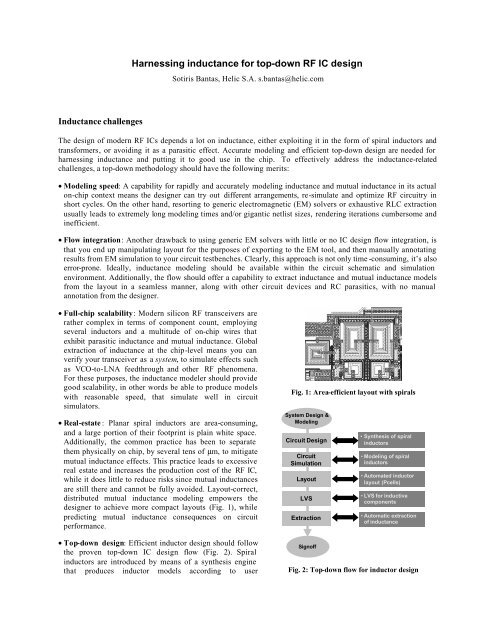
• Real-estate : Planar spiral inductors are area-consuming,<br />
and a large portion of their footprint is plain white space.<br />
Additionally, the common practice has been to separate<br />
them physically on chip, by several tens of µm, to mitigate<br />
mutual <strong>inductance</strong> effects. This practice leads to excessive<br />
real estate and increases the production cost of the <strong>RF</strong> <strong>IC</strong>,<br />
while it does little to reduce risks since mutual <strong>inductance</strong>s<br />
are still there and cannot be fully avoided. Layout-correct,<br />
distributed mutual <strong>inductance</strong> modeling empowers the<br />
<strong>design</strong>er to achieve more compact layouts (Fig. 1), while<br />
predicting mutual <strong>inductance</strong> consequences on circuit<br />
per<strong>for</strong>mance.<br />
• Top-<strong>down</strong> <strong>design</strong>: Efficient inductor <strong>design</strong> should follow<br />
the proven <strong>top</strong>-<strong>down</strong> <strong>IC</strong> <strong>design</strong> flow (Fig. 2). Spiral<br />
inductors are introduced by means of a synthesis engine<br />
that produces inductor models according to user<br />
Fig. 1: Area-efficient layout with spirals<br />
System Design &<br />
Modeling<br />
Circuit Design<br />
Circuit<br />
Simulation<br />
Layout<br />
LVS<br />
Extraction<br />
Signoff<br />
• Synthesis of spiral<br />
inductors<br />
• Modeling of spiral<br />
inductors<br />
• Automated inductor<br />
layout (Pcells)<br />
• LVS <strong>for</strong> inductive<br />
components<br />
• Automatic extraction<br />
of <strong>inductance</strong><br />
Fig. 2: Top-<strong>down</strong> flow <strong>for</strong> inductor <strong>design</strong>
specifications, optimizing metrics such as quality factor, area and placement of leads. Generated inductors are<br />
encapsulated in Pcell definitions, so that they may be easily manipulated by the <strong>design</strong>er by editing geometry<br />
parameters. Pcells can de <strong>design</strong>ed to be always DRC-clean, while complying with foundry-specific <strong>design</strong>-<strong>for</strong>manufacturability<br />
rules (e.g. metal slotting, current carrying limits). When placed and routed in a layout, all<br />
generated inductor instances should pass LVS. For this purpose, special rules should be added to the verification<br />
deck, so that inductor connectivity and geometry can be correctly identified from the layout; otherwise, all spirals<br />
would be treated as plain metal shorts. Finally, at the chip extraction phase inductor models should be<br />
automatically incorporated in the extracted netlist, including all applicable mutual <strong>inductance</strong>; by definition, this<br />
process is non-hierarchical and a special interface should be employed that achieves this in conjunction with the<br />
extraction - verification engine.<br />
Top-<strong>down</strong> <strong>inductance</strong> <strong>design</strong> with Veloce<strong>RF</strong><br />
Veloce<strong>RF</strong> is a Virtuoso®-based toolset [1] that introduces rapid <strong>inductance</strong> modeling, spiral inductor synthesis<br />
and verification <strong>for</strong> <strong>top</strong>-<strong>down</strong> <strong>RF</strong> <strong>IC</strong> <strong>design</strong> flows. It features a spiral inductor synthesis engine, Spiral Wizard<br />
(Fig. 3a), a variety of spiral inductor Pcells (Fig. 3b), and integrated tools <strong>for</strong> inductor characterization (Fig. 4),<br />
netlist extraction from layout (including mutual <strong>inductance</strong>s), modeling of arbitrary metal lines and LVS with<br />
inductor Pcells. Additionally, it provides an Assura interface so that <strong>design</strong>ed inductors can be extracted with full<br />
connectivity in a unified extracted view along with other layout devices and parasitics.<br />
The Veloce<strong>RF</strong> flow collectively addresses the challenges set <strong>for</strong>th previously, by enabling seamless, <strong>top</strong>-<strong>down</strong><br />
<strong>design</strong> of integrated inductors. Its rapid modeling engine produces distributed RLCk netlists and has adequate<br />
capacity to handle large-scale <strong>design</strong>s employing tens of inductors and several interconnect lines.<br />
(a)<br />
(b)<br />
Fig. 3: Veloce<strong>RF</strong> interface in Virtuoso
Fig. 4: Inductor characterization<br />
Showcase: Low-Noise Amplifier (LNA) <strong>design</strong><br />
An LNA <strong>design</strong> testcase is presented. The circuit is tuned in the 2.4-2.5 GHz band and features differential<br />
input/output, inductive source degeneration, LC-tank load and LC impedance matching at the input and output<br />
terminals (Fig. 5). Inductor layout and placement is shown in Fig. 6. Input-matching inductors are optimized <strong>for</strong> Q<br />
with Veloce<strong>RF</strong>’s Spiral Wizard, to achieve a low noise figure. Source degeneration needs low-value inductors, so<br />
these are laid out as ‘half-turn’ spirals. Drain load inductor Pcells were trimmed by the <strong>design</strong>er to an orthogonal<br />
shape, to achieve the required value and center the amplifier’s gain at the desired frequency. Additionally, the<br />
chosen placement minimizes ‘white space’ and achieves a very compact layout (Fig. 7). The final layout was<br />
extracted using Veloce<strong>RF</strong>’s Assura interface, producing an extracted view with encapsulated Veloce<strong>RF</strong> model <strong>for</strong><br />
the inductors. The results from post-layout simulation are given in Fig. 8. The Veloce<strong>RF</strong> modeler takes a about ten<br />
seconds to produce the model <strong>for</strong> all inductors in this layout (including mutual <strong>inductance</strong>s), on a standard P3 Linux<br />
workstation.
V DD<br />
V DD<br />
Bias<br />
L D<br />
OUT P<br />
M 2P<br />
IN P<br />
M 1P<br />
L IN<br />
L S<br />
Source degeneration<br />
paths<br />
Input matching<br />
inductors<br />
Drain Loads/Output<br />
matching inductors<br />
L IN<br />
L S<br />
IN N<br />
M 1N<br />
M 2N<br />
OUT N<br />
Bias<br />
L D<br />
V DD<br />
V DD<br />
Fig. 5: LNA simplified schematic<br />
Fig. 6: Inductor placement<br />
Benefits – discussion<br />
The <strong>top</strong>-<strong>down</strong> methodology implemented in Veloce<strong>RF</strong> provides all the necessary tools <strong>for</strong> <strong>design</strong>ing standard and<br />
custom spiral inductors, and quickly and efficiently transitioning from schematic to final <strong>RF</strong> <strong>IC</strong> layout. The<br />
<strong>inductance</strong> modeling engine is fast, enabling rapid <strong>design</strong> iterations <strong>for</strong> achieving an optimal <strong>design</strong>. Since mutual<br />
<strong>inductance</strong> modeling is available throughout the flow, compact layouts can be achieved that minimize silicon area<br />
without compromising <strong>design</strong> robustness. At the signoff stage of the <strong>design</strong>, the interface seamlessly encapsulates<br />
inductor models to the extracted view, so that the full circuit can be verified <strong>for</strong> <strong>inductance</strong> and mutual <strong>inductance</strong><br />
rapidly and accurately.<br />
References<br />
[1] Sotiris Bantas, Yorgos Koutsoyannopoulos and Apostolos Liapis, “An Inductance Modeling Flow Seamlessly Integrated in<br />
the <strong>RF</strong> <strong>IC</strong> Design Chain,” in Proc. 2004 Design Automation and Test Europe conference (DATE ’04), Paris, Feb. 2004.
Fig. 7: The finalized layout of the LNA<br />
Fig. 8: Post-layout (extracted view) S-parameter response of the LNA