41-660M.pdf - Pickering Interfaces
41-660M.pdf - Pickering Interfaces
41-660M.pdf - Pickering Interfaces

You also want an ePaper? Increase the reach of your titles
YUMPU automatically turns print PDFs into web optimized ePapers that Google loves.
pickering<br />
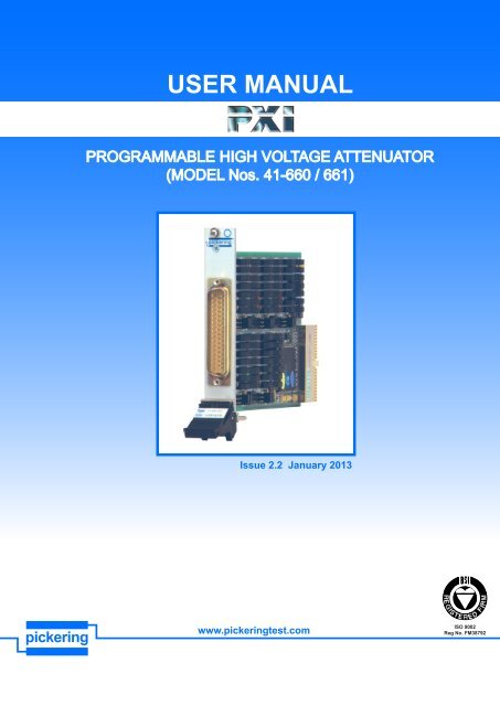
USER MANUAL<br />
PROGRAMMABLE HIGH VOLTAGE ATTENUATOR<br />
(MODEL Nos. <strong>41</strong>-660 / 661)<br />
Issue 2.2 January 2013<br />
pickering<br />
www.pickeringtest.com<br />
ISO 9002<br />
Reg No. FM38792<br />
PROGRAMMABLE HIGH VOLTAGE ATTENUATOR <strong>41</strong>-660/661<br />
Page 1
pickering<br />
© Copyright (2013) <strong>Pickering</strong> <strong>Interfaces</strong>. All Rights Reserved.<br />
No part of this publication may be reproduced, transmitted, transcribed, translated or stored in any form, or<br />
by any means without the written permission of <strong>Pickering</strong> <strong>Interfaces</strong>.<br />
Technical details contained within this publication are subject to change without notice.<br />
Page ii<br />
PROGRAMMABLE HIGH VOLTAGE ATTENUATOR <strong>41</strong>-660/661
pickering<br />
TECHNICAL SUPPORT<br />
For Technical Support please contact <strong>Pickering</strong> <strong>Interfaces</strong> either by phone, fax, the website or via e-mail.<br />
WARRANTY<br />
All products manufactured by <strong>Pickering</strong> <strong>Interfaces</strong> are warranted against defective materials and workmanship for a period of two<br />
years, excluding PXI chassis, from the date of delivery to the original purchaser. Any product found to be defective within this period<br />
will, at the discretion of <strong>Pickering</strong> <strong>Interfaces</strong> be repaired or replaced.<br />
Products serviced and repaired outside of the warranty period are warranted for ninety days.<br />
Extended warranty and service are available. Please contact <strong>Pickering</strong> <strong>Interfaces</strong> by phone, fax, the website or via e-mail.<br />
ENVIRONMENTAL POLICY<br />
<strong>Pickering</strong> <strong>Interfaces</strong> operates under an environmental management system similar to ISO 14001.<br />
<strong>Pickering</strong> <strong>Interfaces</strong> strives to fulfil all relevant environmental laws and regulations and reduce wastes and releases to the<br />
environment. <strong>Pickering</strong> <strong>Interfaces</strong> aims to design and operate products in a way that protects the environment and the health and<br />
safety of its employees, customers and the public. <strong>Pickering</strong> <strong>Interfaces</strong> endeavours to develop and manufacture products that can<br />
be produced, distributed, used and recycled, or disposed of, in a safe and environmentally friendly manner.<br />
Observe the Electrical Hazard Warning detailed in Section 8.<br />
Observe the Electrostatic Sensitive Device Caution detailed in Section 8.<br />
Worldwide Technical Support and Product Information<br />
http://www.pickeringtest.com<br />
<strong>Pickering</strong> <strong>Interfaces</strong> Headquarters<br />
Stephenson Road Clacton-on-Sea CO15 4NL United Kingdom<br />
Tel: +44 (0)1255-687900<br />
Fax: +44 (0)1255-425349<br />
E-Mail: sales@pickeringtest.com<br />
<strong>Pickering</strong> <strong>Interfaces</strong> Inc.<br />
2900 Northwest Vine Street<br />
Grants Pass<br />
Oregon 97526<br />
USA<br />
Tel: +1 5<strong>41</strong> 471 0700<br />
Fax: +1 5<strong>41</strong> 471 8828<br />
E-Mail: ussales@pickeringtest.com<br />
<strong>Pickering</strong> <strong>Interfaces</strong> GmbH<br />
Johann-Karg-Straße 30<br />
D-85540<br />
Haar-Salmdorf<br />
Germany<br />
Tel: +49 89 125 953 160<br />
Fax: +49 89 125 953 189<br />
E-Mail: desales@pickeringtest.com<br />
<strong>Pickering</strong> <strong>Interfaces</strong> AB<br />
Karl Nordströmsväg 31<br />
432 53<br />
Varberg<br />
Sweden<br />
Tel: +46 340-69 06 69<br />
Fax: +46 340-69 06 68<br />
E-Mail: ndsales@pickeringtest.com<br />
<strong>Pickering</strong> <strong>Interfaces</strong> Inc.<br />
(East Coast Regional Office)<br />
67 South Bedford Street, Suite 400W<br />
Burlington, Massachusetts 01803<br />
USA<br />
Tel: +1 781 229 5882<br />
Fax: +1 781 272 0558<br />
E-mail: ussales@pickeringtest.com<br />
<strong>Pickering</strong> <strong>Interfaces</strong> s.r.o.<br />
Smetanova 525<br />
Trinec ˇ<br />
739 61<br />
Czech Republic<br />
Tel: +42 0558 339 168<br />
Fax: +42 0558 340 888<br />
E-mail: cesales@pickeringtest.com<br />
<strong>Pickering</strong> <strong>Interfaces</strong> SARL<br />
6 Rue De La Mare Blanche<br />
77186 Noisiel<br />
Marne Le Vallee<br />
France<br />
Tel +33 1 60 53 55 50<br />
Fax +33 1 60 53 55 99<br />
email frsales@pickeringtest.com<br />
PROGRAMMABLE HIGH VOLTAGE ATTENUATOR <strong>41</strong>-660/661<br />
Page iii
pickering<br />
THIS PAGE INTENTIONALLY BLANK<br />
Page iv<br />
PROGRAMMABLE HIGH VOLTAGE ATTENUATOR <strong>41</strong>-660/661
pickering<br />
CONTENTS<br />
Copyright Statement...........................................................ii<br />
Technical Support and Warranty........................................ iii<br />
Contents (this page)............................................................v<br />
Section 1<br />
Technical Specification.......................................................1.1<br />
Section 2<br />
Technical Description.........................................................2.1<br />
Functional Description.................................................. 2.1<br />
Section 3<br />
Installation...........................................................................3.1<br />
Software Installation.....................................................3.1<br />
Hardware Installation....................................................3.1<br />
Testing............................................................................3.2<br />
Section 4<br />
Programming Guide............................................................4.1<br />
Programming Options For <strong>Pickering</strong> PXI Cards........ 4.1<br />
Soft Front Panel.............................................................4.3<br />
Section 5<br />
Connector Information........................................................5.1<br />
Section 6<br />
Trouble Shooting.................................................................6.1<br />
Section 7<br />
Maintenance Information....................................................7.1<br />
Software Update............................................................7.1<br />
Component Layout........................................................7.1<br />
Section 8<br />
Warnings and Cautions......................................................8.1<br />
PROGRAMMABLE HIGH VOLTAGE ATTENUATOR <strong>41</strong>-660/661<br />
Page v
pickering<br />
THIS PAGE INTENTIONALLY BLANK<br />
Page vi<br />
PROGRAMMABLE HIGH VOLTAGE ATTENUATOR <strong>41</strong>-660/661
pickering<br />
Section 1 - TECHNICAL SPECIFICATION<br />
SECTION 1 - TECHNICAL SPECIFICATION<br />
<strong>41</strong>-660/661<br />
Programmable High Voltage Attenuator<br />
HIGH VOLTAGE ATTENUATOR<br />
<strong>41</strong>-660/661<br />
● High Input Impedance<br />
● 600 Volt Input Rating<br />
● Available With Single or Differential Input<br />
Configurations<br />
● Buffered Single Ended Output Signal<br />
Provides Low Output Impedance<br />
● Wide Output Bandwidth<br />
● High Channel Density<br />
● VISA Drivers Supplied for Windows<br />
XP/Vista/7<br />
● 2 Year Warranty<br />
The <strong>41</strong>-660 and <strong>41</strong>-661 are high voltage attenuators<br />
designed to reduce the high output voltages commonly<br />
generated by some types of sensors. This is in order to<br />
produce manageable signal levels that can be acquired<br />
by typical data acquisition devices in a PXI system.<br />
The <strong>41</strong>-660 provides 10 single ended attenuator<br />
channels while the <strong>41</strong>-661 provides 5 differential<br />
attenuator channels. The attenuated signals are<br />
provided on 50Ω outputs to ensure they can drive<br />
simple data acquisition systems with no significant loss<br />
of signal level. Each model provides attenuation factors<br />
of 10 to 160, permitting a 600V peak signal to be<br />
attenuated to less than 4 Volts.<br />
The <strong>41</strong>-661 attenuates both the common mode and<br />
differential signal equally to ensure the signal cannot<br />
overload the data acquisition system and provides a<br />
single ended output from a difference amplifier.<br />
Attenuation values are controlled by high quality<br />
instrument grade relays to ensure long service life. All<br />
active devices are fully protected against the application<br />
of over-voltages or short circuit loads.<br />
Input<br />
Input A<br />
Input B<br />
Resistor<br />
Ladder<br />
MUX<br />
Buffer<br />
Resistor<br />
Ladder<br />
MUX<br />
MUX<br />
Variable Gain<br />
Difference<br />
Amplifier<br />
Output<br />
Buffer<br />
Block Diagram for the <strong>41</strong>-660 Programmable High<br />
Voltage Attenuator (1 of 10 channels shown)<br />
Output<br />
Resistor<br />
Ladder<br />
Buffer<br />
Block Diagram for the <strong>41</strong>-661 Programmable Differential<br />
High Voltage Attenuator (1 of 5 channels shown)<br />
ISSUE 4.5 APR 2012<br />
PXI Switch & Instrumentation<br />
PROGRAMMABLE <strong>Pickering</strong> HIGH <strong>Interfaces</strong> VOLTAGE www.pickeringtest.com<br />
ATTENUATOR <strong>41</strong>-660/661<br />
Page 1.1
Section 1 - TECHNICAL SPECIFICATION<br />
pickering<br />
Specification<br />
Number of Input Channels<br />
<strong>41</strong>-660:<br />
<strong>41</strong>-661:<br />
Maximum Input Voltage: ±600V<br />
Input Impedance<br />
<strong>41</strong>-660:<br />
<strong>41</strong>-661 (Differential):<br />
<strong>41</strong>-661 (Common Mode):<br />
Attenuation Values:<br />
Attenuation Accuracy:<br />
Output Offset Voltage<br />
<strong>41</strong>-660:<br />
<strong>41</strong>-661:<br />
Output Impedance:<br />
Output Voltage (Max):<br />
Output Current:<br />
Output Bandwidth:<br />
Output Slew Rate:<br />
PCI Interface:<br />
Programming<br />
All PXI modules are supplied with complete Windows XP/Vista/7<br />
drivers, these perform the following functions:-<br />
• Write word/s to module (to set relay pattern)<br />
• Write bit to module (to operate an individual relay)<br />
• Full relay status reporting<br />
• Module identification and location information<br />
• Set and read module calibration information<br />
Up to date driver software is available from our web site at<br />
www.pickeringtest.com<br />
Power Requirements<br />
+3.3V +5V +12V -12V<br />
0 0.5A max 0.15A max 0.15A max<br />
Width and Dimensions<br />
Size:<br />
Connectors<br />
PXI bus:<br />
Front panel connector:<br />
10 off (Single Ended)<br />
5 off (Differential)<br />
1MΩ<br />
0.666MΩ<br />
0.5MΩ<br />
10, 20, 40, 80 or 160<br />
1% excluding DC offset<br />
pickering<br />
Section 2 - TECHNICAL DESCRIPTION<br />
SECTION 2 - TECHNICAL DESCRIPTION<br />
Functional Description<br />
A functional block diagram is provided in Figure 2.1. The Module is powered by a +5V input via Compact PCI<br />
connector J1. The signal interface to the attenuator is via the front panel mounted 50-way D-type male connector, J2.<br />
The module comprises a PCB populated with 10 resistor ladders which perform the attenuation function, followed by<br />
10 buffer amplifiers and - in the case of the <strong>41</strong>-661 - 5 variable gain differential amplifiers. The resistor ladders and<br />
the gain of the differential amplifiers are controlled by reed relays. The relays are energised via signals from relay<br />
drivers U8 to U12, the relay drivers have data latched into them from the control logic which in turn is addressed by<br />
PCI bridge U1. Module configuration is determined by hardwired links and data stored in EEPROM U7. PCI Bridge<br />
U1 is configured by EEPROM U2.<br />
50-WAY D-TYPE<br />
CONNECTOR<br />
J2<br />
ATTENUATOR<br />
RELAY<br />
CONTACTS<br />
RELAY COILS<br />
COMPACT PCI<br />
BUS<br />
CONNECTOR<br />
J1<br />
RELAY<br />
DRIVERS<br />
U8, U9,<br />
U10, U11,<br />
U12<br />
CONTROL<br />
LOGIC<br />
U3, U4,<br />
U5, U6<br />
PCI<br />
BRIDGE<br />
U1<br />
TERMINATING<br />
RESISTORS<br />
R6 TO R17<br />
MODULE<br />
CONFIGURATION<br />
U7<br />
+5V<br />
0V<br />
PCI BRIDGE<br />
CONFIGURATION<br />
U2<br />
<strong>41</strong>-660 SINGLE-ENDED ATTENUATOR INPUT A<br />
<strong>41</strong>-661 DIFFERENTIAL ATTENUATOR<br />
INPUT<br />
RESISTOR<br />
LADDER<br />
BUFFER<br />
AMPLIFIER<br />
DIFFERENTIAL<br />
AMPLIFIER<br />
RESISTOR<br />
LADDER<br />
BUFFER<br />
AMPLIFIER<br />
OUTPUT<br />
GND<br />
INPUT B<br />
OUTPUT<br />
GND<br />
X10<br />
RESISTOR<br />
LADDER<br />
BUFFER<br />
AMPLIFIER<br />
GAIN<br />
SWITCHING<br />
GND<br />
X5<br />
Figure 2.1 - Programmable Attenuator Module (<strong>41</strong>-660/661): Functional Block Diagram<br />
PROGRAMMABLE HIGH VOLTAGE ATTENUATOR <strong>41</strong>-660/661<br />
Page 2.1
Section 2 - TECHNICAL DESCRIPTION<br />
pickering<br />
THIS PAGE INTENTIONALLY BLANK<br />
Page 2.2<br />
PROGRAMMABLE HIGH VOLTAGE ATTENUATOR <strong>41</strong>-660/661
pickering<br />
Section 3 - INSTALLATION<br />
SECTION 3 - INSTALLATION<br />
Software Installation<br />
First install the appropriate <strong>Pickering</strong> PXI switch module drivers by running the installer program Setup.exe, either<br />
from the CD-ROM supplied, or by downloading the latest version from our website http://www.pickeringtest.com -<br />
the recommended method. There are different versions of the Setup program to suit different Windows versions<br />
and software environments. Setup is accompanied by a ReadMe file containing additional installation information.<br />
A single installation covers all modules in the System 40, System 45 and System 50 ranges.<br />
When installation completes, the installed drivers’ ReadMe file is offered for display. It can also be displayed later<br />
using a shortcut on the Programs>><strong>Pickering</strong> menu.<br />
If you are not a LabVIEW user you should choose the “full” version, and once that has been installed run the<br />
LabVIEW Runtime Engine installer via the shortcut on the Programs>><strong>Pickering</strong> menu. In the absence of LabVIEW<br />
the Runtime Engine is required to support the <strong>Pickering</strong> Test Panels application.<br />
Hardware Installation<br />
CAUTION<br />
Electrostatic discharge can damage the components on the module. To avoid such damage in handling the board,<br />
touch the anti-static bag to a metal part of the chassis before removing the board from the bag.<br />
Ensure that there is adequate ventilation in accordance with the PXI Specification.<br />
The module should be installed in accordance with the following procedure:<br />
1. Ensure that the system is turned OFF but still connected to mains so that it remains grounded.<br />
2. Choose an appropriate slot in the rack.<br />
3. Remove the blanking plate for the chosen slot.<br />
4. Ensure that the injector/ejector handle is in its downward position. Align the module with the card guides on<br />
the top and bottom of the slot.<br />
WARNING: Do not raise the injector/ejector handle whilst inserting the module. The module will not insert<br />
properly unless the handle is in its downward position.<br />
5. Hold the handle whilst slowly sliding the module into the card guides until the handle catches on the injector/<br />
ejector rail (refer to Figure 3.1).<br />
6. Raise the injector/ejector handle until the module firmly seats into the backplane. The front panel of the<br />
module should be flush with the front panel of the chassis.<br />
7. Screw the front panel of the module to the front panel mounting rail.<br />
8. In a system employing MXI-3 to connect a desktop PC to a PXI chassis or to link multiple chassis, power-up<br />
the system as follows:<br />
a. For a system comprising a PC and one chassis, power up the chassis before powering up the PC.<br />
b. For a system comprising more than one chassis, turn ON the last chassis in the system followed by the<br />
penultimate, etc, and finally turn ON the PC or chassis containing the system controller.<br />
9. For <strong>Pickering</strong> <strong>Interfaces</strong> modular LXI installation there is no requirement to use any particular power up<br />
sequence.<br />
PROGRAMMABLE HIGH VOLTAGE ATTENUATOR <strong>41</strong>-660/661<br />
Page 3.1
Section 3 - INSTALLATION<br />
pickering<br />
PXI / LXI Chassis<br />
Figure 3.1 - Installing the<br />
module into a PXI / cPCI / LXI<br />
Chassis<br />
Testing Operation<br />
Figure 3.1 - Installing the module into a PXI/Compact PCI Chassis<br />
Start the Test Panels application from the Programs>><strong>Pickering</strong>>>PXI Utilities menu. If you are a LabVIEW user, run<br />
“Test Panels (LabVIEW VI)”; if not, run “Test Panels (EXE)”. A selector panel will appear, listing all installed <strong>Pickering</strong><br />
PXI switch modules. Click on the module you wish to control, and a graphical control panel is presented allowing<br />
operation of the module. Panels can be opened simultaneously for all the installed modules.<br />
Figure 3.2 - Typical Test Panel Display<br />
As an alternative to the Test Panels, the simple Terminal Monitor program PILMon (again on the<br />
Programs>><strong>Pickering</strong>>>PXI Utilities menu) allows access to all functions of <strong>Pickering</strong> switch modules through a<br />
command-line interface. In PILMon, enter “HE” for help on it’s commands.<br />
Please note that both the Test Panels and Terminal Monitor gain exclusive access to the modules, and so only one<br />
of them can be operational at any time.<br />
Page 3.2<br />
PROGRAMMABLE HIGH VOLTAGE ATTENUATOR <strong>41</strong>-660/661
pickering<br />
Section 4 - PROGRAMMING GUIDE<br />
SECTION 4 - PROGRAMMING GUIDE<br />
Programming options for <strong>Pickering</strong> <strong>Interfaces</strong> PXI Cards<br />
Software drivers are supplied for Microsoft Windows XP/Vista/7 operating systems, with specific support for the<br />
following development environments:<br />
●●<br />
●●<br />
●●<br />
●●<br />
Microsoft Visual Studio (VB, C++, C#)<br />
Borland C++<br />
National Instruments LabWindows/CVI<br />
National Instruments LabVIEW and LabVIEW RT<br />
Windows drivers are supplied in the form of Dynamic Link Libraries, which should also be usable in any other<br />
development environment that supports them.<br />
Some recent drivers developed for the LXI platform are capable of addressing both PXI and LXI domains. Such<br />
duality may be of help to users considering future migration from PXI based systems to LXI based systems, or<br />
indeed systems containing both PXI and LXI components.<br />
Programming for PXI<br />
A number of different Windows drivers are available to meet particular system requirements, and should none of<br />
these be suitable there is also the option of register-level programming. Drivers are generally ‘universal’, handling all<br />
models in the System 40, 45 and 50 ranges; however some models that are not compliant with the Ivi Swtch class<br />
cannot be used with the pi40iv IVI driver. The pipx40 and Pilpxi drivers are also applicable to certain models in the<br />
System <strong>41</strong> (PXI Instruments) range - see these drivers’ System <strong>41</strong> support list.<br />
Please note that this documentation is available in its most up-to-date form as HTML help files, fully hyperlinked for<br />
easy access - both pipx40 and Pilpxi documents are included in the Pipx40vpp software installation.<br />
VISA Driver for Windows - pipx40<br />
The pipx40 driver conforms to the VISA (Virtual Instrument Software Architecture) standard for programmable<br />
instrumentation. Instrument control environments such as LabVIEW and LabWindows/CVI are based on VISA, and<br />
pipx40 support libraries are provided for them.<br />
Prior installation of VISA from National Instruments is required for the operation of this driver.<br />
Where VISA is available, pipx40 can also be used in general-purpose programming environments such as Visual<br />
C++ and Visual Basic. When IVI is not a system requirement this driver will often yield faster operation than the<br />
pi40iv driver.<br />
Direct I/ODriver for Windows - Pilpxi<br />
The Pilpxi driver accesses cards directly, without using the VISA software layer, while offering similar overall<br />
functionality to pipx40. It is most commonly used in general-purpose programming environments such as Visual<br />
C++ and Visual Basic. Operating speed of the VISA and Direct I/O drivers is generally comparable.<br />
Register-level Programming<br />
Where the supplied drivers are not suitable, register-level programming can be employed - for example:<br />
●●<br />
●●<br />
●●<br />
●●<br />
If the functionality of the supplied drivers does not meet the application requirements<br />
If security considerations demand full source-code for the application<br />
In development environments that have alternate mechanisms for accessing PCI bus<br />
For operating systems other than Windows<br />
PROGRAMMABLE HIGH VOLTAGE ATTENUATOR <strong>41</strong>-660/661<br />
Page 4.1
Section 4 - PROGRAMMING GUIDE<br />
pickering<br />
General <strong>Pickering</strong> Card Architecture<br />
With most drivers, before programming a <strong>Pickering</strong> card it is important to understand the basic architecture of<br />
<strong>Pickering</strong> cards.<br />
The switches on a <strong>Pickering</strong> card are organized into logical sub-units, each sub-unit containing a set of objects of<br />
similar type and use. These objects may be switches, digital outputs, digital inputs, resistors, power supplies etc,<br />
depending on the nature of the specific card.<br />
For example a simple matrix card will usually contain a single sub-unit containing the switches arranged in a<br />
2-dimensional array. However a similar card with additional isolating relays connected to the matrix will contain<br />
additional sub-units containing those isolation relays.<br />
Low level drivers include functions to allow the programmer to query the card to ascertain the number of sub-units,<br />
and the size and type of each sub-unit.<br />
For full details of the driver functions available the programmer should refer to the documentation provided.<br />
Soft FRONT PANEL<br />
The installation CD supplied with the module also includes a Soft Front Panel which can be run on a PC under<br />
Windows. This allows straightforward graphical control of the attenuation function of each channel - an example of<br />
this is shown in Figure 4.1.<br />
Figure 4.1 - Soft Front Panel for the Attenuator Module<br />
Page 4.2<br />
PROGRAMMABLE HIGH VOLTAGE ATTENUATOR <strong>41</strong>-660/661
pickering<br />
Section 5 - CONNECTOR INFORMATION<br />
SECTION 5 - CONNECTOR INFORMATION<br />
The front panel connector on the <strong>41</strong>-660 and <strong>41</strong>-661 Programmable Attenuator modules is shown in Figure 5.1.<br />
The pin-out for the <strong>41</strong>-660 Single Ended Attenuator is shown in Figure 5.2 and the pin-out for the <strong>41</strong>-661 Differential<br />
Attenuator is shown in Figure 5.3.<br />
pickering<br />
Figure 5.1 - Programmable Attenuator Module <strong>41</strong>-660/661: Front Panel<br />
PROGRAMMABLE HIGH VOLTAGE ATTENUATOR <strong>41</strong>-660/661<br />
Page 5.1
Section 5 - CONNECTOR INFORMATION<br />
pickering<br />
<strong>41</strong>-660-001 50-Way D-Type Plug<br />
34<br />
35<br />
36<br />
37<br />
38<br />
39<br />
40<br />
<strong>41</strong><br />
42<br />
43<br />
44<br />
45<br />
46<br />
47<br />
48<br />
49<br />
50<br />
18<br />
19<br />
20<br />
21<br />
22<br />
23<br />
24<br />
25<br />
26<br />
27<br />
28<br />
29<br />
30<br />
31<br />
32<br />
33<br />
1<br />
2<br />
3<br />
4<br />
5<br />
6<br />
7<br />
8<br />
9<br />
10<br />
11<br />
12<br />
13<br />
14<br />
15<br />
16<br />
17<br />
Pin<br />
Number<br />
Signal<br />
Name<br />
Pin<br />
Number<br />
Signal<br />
Name<br />
Pin<br />
Number<br />
Signal<br />
Name<br />
34 CH1 I/P 18 CH5 I/P 1 CH9 I/P<br />
35 GND 19 GND 2 GND<br />
36 CH2 I/P 20 CH6 I/P 3 CH10 I/P<br />
37 GND 21 GND 4 GND<br />
38 CH1 O/P 22 CH5 O/P 5 CH9 O/P<br />
39 GND 23 GND 6 GND<br />
40 CH2 O/P 24 CH6 O/P 7 CH10 O/P<br />
<strong>41</strong> GND 25 GND 8 GND<br />
42 GND 26 CH7 I/P 9 GND<br />
43 CH3 I/P 27 GND 10 NC<br />
44 GND 28 CH8 I/P 11 NC<br />
45 CH4 I/P 29 GND 12 NC<br />
46 GND 30 CH7 O/P 13 NC<br />
47 CH3 O/P 31 GND 14 NC<br />
48 GND 32 CH8 O/P 15 NC<br />
49 CH4 O/P 33 GND 16 NC<br />
50 GND 17 NC<br />
50-WAY D-TYPE PLUG<br />
Figure 5.2 - Single Ended Programmable Attenuator Module <strong>41</strong>-660-001: Pin-Out<br />
<strong>41</strong>-661-001 50-Way D-Type Plug<br />
34<br />
35<br />
36<br />
37<br />
38<br />
39<br />
40<br />
<strong>41</strong><br />
42<br />
43<br />
44<br />
45<br />
46<br />
47<br />
48<br />
49<br />
50<br />
18<br />
19<br />
20<br />
21<br />
22<br />
23<br />
24<br />
25<br />
26<br />
27<br />
28<br />
29<br />
30<br />
31<br />
32<br />
33<br />
1<br />
2<br />
3<br />
4<br />
5<br />
6<br />
7<br />
8<br />
9<br />
10<br />
11<br />
12<br />
13<br />
14<br />
15<br />
16<br />
17<br />
Pin<br />
Number<br />
Signal<br />
Name<br />
Pin<br />
Number<br />
Signal<br />
Name<br />
Pin<br />
Number<br />
Signal<br />
Name<br />
34 CH1 I/P 1 18 CH3 I/P 1 1 CH5 I/P 1<br />
35 GND 19 GND 2 GND<br />
36 CH1 I/P 2 20 CH3 I/P 2 3 CH5 I/P 2<br />
37 GND 21 GND 4 GND<br />
38 NC 22 NC 5 NC<br />
39 CH1 O/P 23 CH3 O/P 6 CH5 O/P<br />
40 NC 24 NC 7 NC<br />
<strong>41</strong> GND 25 GND 8 GND<br />
42 GND 26 CH4 I/P 1 9 GND<br />
43 CH2 I/P 1 27 GND 10 NC<br />
44 GND 28 CH4 I/P 2 11 NC<br />
45 CH2 I/P 2 29 GND 12 NC<br />
46 GND 30 NC 13 NC<br />
47 NC 31 CH4 O/P 14 NC<br />
48 CH2 O/P 32 NC 15 NC<br />
49 NC 33 GND 16 NC<br />
50 GND 17 NC<br />
50-WAY D-TYPE PLUG<br />
Figure 5.3 - Differential Programmable Attenuator Module <strong>41</strong>-661-001: Pin-Out<br />
Page 5.2<br />
PROGRAMMABLE HIGH VOLTAGE ATTENUATOR <strong>41</strong>-660/661
pickering<br />
SECTION 6 - TROUBLE SHOOTING<br />
SECTION 6 - TROUBLESHOOTING<br />
Installation Problems<br />
The Plug & Play functionality of <strong>Pickering</strong> switch cards generally ensures trouble-free installation.<br />
If you do experience any installation problems you should first ensure that all cards are properly seated in their slots.<br />
Improperly mated cards may go undetected by the operating system, or may be detected as a card of an unknown<br />
type. They can also cause the computer to freeze at various stages in the boot sequence.<br />
If your system employs MXI-3 you should check the integrity of all MXI-3 links. When the system is powered up, and<br />
during Windows start-up, you should expect to see periodic activity on the MXI-3 RX/TX (yellow) indicators, clearing<br />
to leave only the PWR/LNK (green) LEDs illuminated. The RX/TX indicators should show activity when you attempt<br />
to access a card.<br />
Diagnostic Utility<br />
The <strong>Pickering</strong> Diagnostic Utility (accessible through the Programs>><strong>Pickering</strong>>>PXI Utilities menu) generates a<br />
diagnostic report of the system’s PCI configuration, highlighting any potential configuration problems. Specific details<br />
of all installed <strong>Pickering</strong> switch cards are included. All the installed <strong>Pickering</strong> switch cards should be listed in the<br />
“Pilpxi information” section - if one or more cards is missing it may be possible to determine the reason by referring to<br />
the PCI configuration dump contained in the report, but interpretation of this information is far from straightforward,<br />
and the best course is to contact <strong>Pickering</strong> support: support@pickeringtest.com, if possible including a copy of the<br />
diagnostic report.<br />
In the “VISA information” section, if VISA is not installed it’s absence will be reported. This does not affect operation<br />
using the Direct I/O driver, and is not a problem unless you wish to use VISA. VISA is a component of National<br />
Instruments LabWindows/CVI and LabVIEW, or is available as a standalone environment.<br />
If VISA is present and is of a sufficiently recent version, the section “Pipx40 information” should present a listing<br />
similar to “Pilpxi information”.<br />
Please note that the Diagnostic Utility cannot access cards if they are currently opened by some other application,<br />
such as the Test Panels or Terminal Monitor.<br />
PROGRAMMABLE HIGH VOLTAGE ATTENUATOR <strong>41</strong>-660/661 Page 6.1
SECTION 6 - TROUBLE SHOOTING<br />
pickering<br />
THIS PAGE INTENTIONALLY BLANK<br />
Page 6.2<br />
PROGRAMMABLE HIGH VOLTAGE ATTENUATOR <strong>41</strong>-660/661
pickering<br />
Section 7 - MAINTENANCE INFORMATION<br />
SECTION 7 - MAINTENANCE INFORMATION<br />
SOFTWARE UPDATE<br />
For PXI modules operating in a PXI chassis, no module software updates are required. For the latest version of<br />
the driver please refer to our web site www.pickeringtest.com where links to our Software Download page will<br />
provide the latest version of the driver software for the various programming environments encountered.<br />
For PXI modules which are supported in one of <strong>Pickering</strong> <strong>Interfaces</strong>’ Modular LXI Chassis (such as the 60-102<br />
and 60-103) no module software update is required. If the module was introduced after the LXI chassis was<br />
manufactured the module may not be recognized, in this case the chassis firmware may need upgrading. This<br />
is a simple process which is described in the manual for the Modular LXI Chassis.<br />
COMPONENT LAYOUT<br />
The component Layout is as detailed in Figures 7.1 and 7.2.<br />
Figure 7.1 - Programmable High Voltage Attenuator<br />
PROGRAMMABLE HIGH VOLTAGE ATTENUATOR <strong>41</strong>-660/661<br />
Page 7.1
Section 7 - MAINTENANCE INFORMATION<br />
pickering<br />
RL1<br />
RL8<br />
RL33<br />
RL40<br />
RL65<br />
RL72<br />
RL2<br />
RL9<br />
RL34<br />
RL<strong>41</strong><br />
RL66<br />
RL73<br />
RL3<br />
RL10<br />
RL35<br />
RL42<br />
RL67<br />
RL74<br />
RL4<br />
RL11<br />
RL36<br />
RL43<br />
RL68<br />
RL75<br />
RL5<br />
RL12<br />
RL37<br />
RL44<br />
RL69<br />
RL76<br />
RL6<br />
RL13<br />
RL38<br />
RL45<br />
RL70<br />
RL77<br />
RL7<br />
RL14<br />
RL39<br />
RL46<br />
RL71<br />
RL78<br />
RL17<br />
RL24<br />
RL49<br />
RL56<br />
RL18<br />
RL25<br />
RL50<br />
RL57<br />
RL19<br />
RL26<br />
RL51<br />
RL58<br />
RL20<br />
RL27<br />
RL52<br />
RL59<br />
RL21<br />
RL28<br />
RL53<br />
RL60<br />
RL22<br />
RL29<br />
RL54<br />
RL61<br />
RL23<br />
RL30<br />
RL55<br />
RL62<br />
RL31<br />
RL32<br />
RL63<br />
RL64<br />
RL15<br />
RL16<br />
RL47<br />
RL48<br />
RL79<br />
RL80<br />
Figure 7.2 - Programmable High Voltage Attenuator: Component Layout<br />
Page 7.2<br />
PROGRAMMABLE HIGH VOLTAGE ATTENUATOR <strong>41</strong>-660/661
pickering<br />
Section 8 - CAUTIONS<br />
SECTION 8 - WARNINGS AND CAUTIONS<br />
WARNING – HAZARDOUS ENVIRONMENTS<br />
This product is not specifically designed for use in hazardous<br />
environments, for example in explosive atmospheres. If the product is to<br />
be used in hazardous environments we recommend that the user ensures<br />
suitable protective measures are taken.<br />
WARNING - DANGER OF ELECTRIC SHOCK<br />
THIS MODULE MAY CONTAIN HAZARDOUS VOLTAGES. BEFORE REMOVING<br />
THE MODULE FROM THE RACK REMOVE ALL SUPPLIES.<br />
CAUTION – Handling of Electrostatic-Sensitive Semiconductor Devices<br />
Certain semiconductor devices used in this equipment are liable to damage due to static<br />
voltage. Observe the following precautions when handling these devices in their unterminated<br />
state, or sub-units containing these devices:<br />
1. Persons removing sub-units from an equipment using these devices must be earthed by a<br />
wrist strap and a resistor at the point provided on the equipment.<br />
2. Soldering irons used during the repair operations must be low voltage types with earthed<br />
tips and isolated from the mains voltage by a double insulated transformer.<br />
3. Outer clothing worn must be unable to generate static charges.<br />
4.<br />
Printed Circuit Boards (PCBs) fitted with these devices must be stored and transported in<br />
anti-static bags.<br />
PROGRAMMABLE HIGH VOLTAGE ATTENUATOR <strong>41</strong>-660/661<br />
Page 8.1
pickering<br />
THIS PAGE INTENTIONALLY BLANK<br />
Page 8.2<br />
PROGRAMMABLE HIGH VOLTAGE ATTENUATOR <strong>41</strong>-660/661