
Create successful ePaper yourself
Turn your PDF publications into a flip-book with our unique Google optimized e-Paper software.
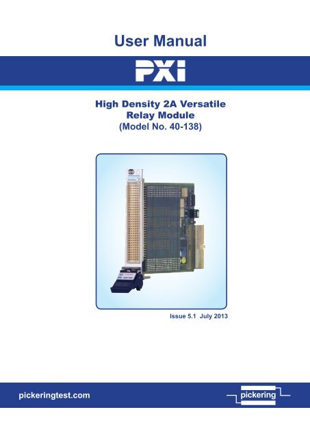
pickeringUser ManualHigh Density 2A VersatileRelay Module(Model No. <strong>40</strong>-138)Issue 5.1 July 2013pickeringtest.compickeringHIGH DENSITY 2A VERSATILE RELAY MODULE <strong>40</strong>-138Page 1
pickering© COPYRIGHT (2013) PICKERING INTERFACES. ALL RIGHTS RESERVED.No part of this publication may be reproduced, transmitted, transcribed, translated or stored in any form, orby any means without the written permission of <strong>Pickering</strong> <strong>Interfaces</strong>.Technical details contained within this publication are subject to change without notice.ISO 9001Reg No. FM38792Page iiHIGH DENSITY 2A VERSATILE RELAY MODULE <strong>40</strong>-138
pickeringpickeringteChNICal sUPPortFor Technical Support please contact <strong>Pickering</strong> <strong>Interfaces</strong> either by phone, fax, the website or via e-mail.WarraNtyAll products manufactured by <strong>Pickering</strong> <strong>Interfaces</strong> are warranted against defective materials and workmanship for a period ofthree years, excluding programmable power supplies, from the date of delivery to the original purchaser. Any product found to bedefective within this period will, at the discretion of <strong>Pickering</strong> <strong>Interfaces</strong> be repaired or replaced.Products serviced and repaired outside of the warranty period are warranted for ninety days.Extended warranty and service are available. Please contact <strong>Pickering</strong> <strong>Interfaces</strong> by phone, fax, the website or via e-mail.eNvIroNMeNtal PolICy<strong>Pickering</strong> <strong>Interfaces</strong> operates under an environmental management system similar to ISO 1<strong>40</strong>01.<strong>Pickering</strong> <strong>Interfaces</strong> strives to fulfil all relevant environmental laws and regulations and reduce wastes and releases to theenvironment. <strong>Pickering</strong> <strong>Interfaces</strong> aims to design and operate products in a way that protects the environment and the health andsafety of its employees, customers and the public. <strong>Pickering</strong> <strong>Interfaces</strong> endeavours to develop and manufacture products that canbe produced, distributed, used and recycled, or disposed of, in a safe and environmentally friendly manner.Observe the Electrical Hazard Warning detailed in Section 8.Observe the Electrostatic Sensitive Device Caution detailed in Section 8.Worldwide Technical Support and Product Informationhttp://www.pickeringtest.com<strong>Pickering</strong> <strong>Interfaces</strong> HeadquartersStephenson Road Clacton-on-Sea CO15 4NL United KingdomTel: +44 (0)1255-687900Fax: +44 (0)1255-425349E-Mail: sales@pickeringtest.com<strong>Pickering</strong> <strong>Interfaces</strong> Inc.2900 Northwest vine streetgrants Passoregon 97526Usatel: +1 541 471 0700Fax: +1 541 471 8828e-Mail: ussales@pickeringtest.com<strong>Pickering</strong> <strong>Interfaces</strong> gmbhJohann-karg-straße 30d-855<strong>40</strong>haar-salmdorfgermanytel: +49 89 125 953 160Fax: +49 89 125 953 189e-Mail: desales@pickeringtest.com<strong>Pickering</strong> <strong>Interfaces</strong> aBkarl Nordströmsväg 31432 53varbergswedentel: +46 3<strong>40</strong>-69 06 69Fax: +46 3<strong>40</strong>-69 06 68e-Mail: ndsales@pickeringtest.com<strong>Pickering</strong> <strong>Interfaces</strong> Inc.(east Coast regional office)67 south Bedford street, suite <strong>40</strong>0WBurlington, Massachusetts 01803Usatel: +1 781 229 5882Fax: +1 781 272 0558e-mail: ussales@pickeringtest.com<strong>Pickering</strong> <strong>Interfaces</strong> s.r.o.smetanova 525trinec ˇ739 61Czech republictel: +420 558 987 613Fax: +420 558 987 601e-mail: desales@pickeringtest.com<strong>Pickering</strong> <strong>Interfaces</strong> sarl6 rue de la Mare Blanche77186 NoisielMarne le valleeFrancetel +33 1 60 53 55 50Fax +33 1 60 53 55 99email frsales@pickeringtest.com2 HIGH AMP DENSITY 1-Pole HIGH 2A VERSATILE DeNSITY MATRIX RELAY <strong>40</strong>-528/529 MODULE <strong>40</strong>-138Page iii
pickeringTHIS PAGE INTENTIONALLY BLANKPage ivHIGH DENSITY 2A VERSATILE RELAY MODULE <strong>40</strong>-138
pickeringCONTENTSCopyright Statement...........................................................iiTechnical Support and Warranty........................................ iiiContents (this page)............................................................vSection 1Technical Specification.......................................................1.1Section 2Technical Description.........................................................2.1Functional Description.................................................. 2.1Guidance on Power Handling....................................... 2.2Section 3Installation...........................................................................3.1Hardware Installation.................................................... 3.1Software Installation.....................................................3.2Section 4Programming Guide............................................................4.1Programming Options For <strong>Pickering</strong> PXI Cards........ 4.1Module Architecture...................................................... 4.3Programming The Module............................................ 4.3Section 5Connector Information........................................................5.1Section 6Trouble Shooting.................................................................6.1Section 7Maintenance Information.................................................... 7.1Software Update............................................................7.1Relay Lookup Tables.....................................................7.2Section 8Warnings and Cautions...................................................... 8.1Appendix AExample Connector Pinouts.............................................. A.1HIGH DENSITY 2A VERSATILE RELAY MODULE <strong>40</strong>-138Page v
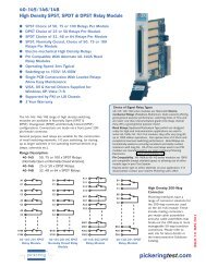
pickeringSECTION 1 - TECHNICAL SPECIFICATIONSECTION 1 - TECHNICAL SPECIFICATION<strong>40</strong>-138High Density 2A Versatile Relay Module● VERSATILE CELL-BASED DESIGN ALLOWSSLOT-SAVING HIGH DENSITY MIXEDCONFIGURATIONS● Mixed Relay Configurations With AnyCombination of SPST, DPST, SPDT & DPDT● Maximum Current 2A Hot or Cold Switching● Switch up to 300VDC/250VAC and up to60W Max Power● Reduced Cost Partially Populated VersionsAvailable● VISA, IVI & Kernel Drivers Supplied forWindows XP/Vista/7/8● Supported by PXI or LXI Chassis● 3 Year WarrantyThe <strong>40</strong>-138 2A Relay Series is suitable for applicationsrequiring medium power switching with high density.Featuring 2A current capacity and voltages to300VDC/250VAC, the <strong>40</strong>-138 provides a broadselection of mixed relay types for greater flexibility.The module consists of 13 cells which can be specifiedas empty or populated with one relay type. Theavailable types are:* SPST (Single Pole Single Throw) - 6 per cell.* DPST (Double Pole Single Throw) - 3 per cell.* SPDT (Single Pole Double Throw) - 4 per cell.* DPDT (Double Pole Double Throw) - 2 per cell.The permissible arrangement of cells is shown is theconfiguration example overleaf.Mixed configurations are very useful for high densityand/or low cost applications where optimum usagemust be made of all relays, and where there arevery few PXI slots available. The <strong>40</strong>-138 can beused for replacing legacy VXI or custom switch cardswhere mixed relay types have been deployed. If aconfiguration is required with only one switch type,please refer to the data sheet for the <strong>40</strong>-139. Thisoffers high density low cost solutions with 2 Ampelectro-mechanical relays.Connections are made via a front panel mounted160 way DIN 41612 high density connector. <strong>Pickering</strong>also provide a wide range of connector and cablingsolutions, refer to <strong>Pickering</strong>’s “Interconnection Catalog”or visit our web site.Typical applications will be found in Automotive,Aerospace, Military and Power Cell Testing applications.B1A1A1C1C1BB2ACaa xA2C2ACbb x cc x dd x<strong>40</strong>-138 Versatile Mixed Relay Moduleaa x SPST, bb x DPST, cc x SPDT, dd x DPDTA2C2ISSUE 5.0 MAY 2013HIGH DENSITY 2A VERSATILE RELAY MODULE <strong>40</strong>-138pickeringtest.comPage 1.1
SECTION 1 - TECHNICAL SPECIFICATIONpickering<strong>40</strong>-138 Mixed Relay ConfiguratorWhen ordering a configuration of mixed relays, each cell canbe set to be populated by SPST, DPST, SPDT or DPDT. Thepart number is in the form <strong>40</strong>-138-aa-bb-cc-dd where:aa is the number of SPST relays (multiples of 6)bb is the number of DPST relays (multiples of 3)cc is the number of SPDT relays (multiples of 4)dd is the number of DPDT relays (multiples of 2)For further assistance consult the Operating Manual, web siteor contact sales office.Relay Type Cells 1 to 13 Cell 13 custom build†SPST 6 per cell 8DPST 3 per cell 4SPDT 4 per cell 4DPDT 2 per cell 2† Note: Cell 13 is configured as the same size as other cells except oncustom builds.<strong>40</strong>-138 Mixed Relay Configuration ExampleA typical mixed relay example is shown in the followingtable where the specified configuration is; 12 x SPST, 15x DPST, 16 x SPDT and 4 x DPDT. This corresponds tothe order code: <strong>40</strong>-138-12-15-16-4. SPST switches arealways installed in the lowest cell number and DPDT arealways installed in the highest populated cell number.For further assistance please contact sales office.RelayTypeCell 1Cell 2Cell 3Cell 4Cell 5Cell 6Cell 7Cell 8Cell 9Cell 10Cell 11Cell 12Cell 13TotalSPST 6 6 6 6 6 6 6 6 6 6 6 6 8 12DPST 3 3 3 3 3 3 3 3 3 3 3 3 4 15SPDT 4 4 4 4 4 4 4 4 4 4 4 4 4 16DPDT 2 2 2 2 2 2 2 2 2 2 2 2 2 4A1C1A2C2A3C3A4C4A5C5A6C6A7C7A8C8A9C9A10C10A11C11A12C12A1.1The above configuration is shown in the diagram below.C1.1A1.2C1.2A2.1A9.1B1B9C2.1C9.1A1A9A2.2A9.2C1C9B1.1C2.2C9.2A1.1A3.1A10.1B2B10C1.1C3.1C10.1A2A10B1.2A3.2A10.2C2C10A1.2C3.2C10.2B3B11C1.2A4.1A11.1A3A11C4.1C11.1B2.1C3C11A4.2A11.2A2.1C4.2C11.2B4B12C2.1A5.1A12.1A4A12B2.2C5.1C12.1C4C12A2.2A5.2A12.2C2.2B5B13C5.2C12.2A5A13B3.1A6.1A13.1C5C13A3.1C6.1C13.1C3.1A6.2A13.2B6B14B3.2C6.2C13.2A6A14A3.2A7.1A14.1C6C14C3.2C7.1C14.1B7B15A7.2A14.2B4.1A7A15C7.2C14.2A4.1C7C15A8.1A15.1C4.1C8.1A8.2C8.2C15.1A15.2C15.2B8A8C8B16A16C16B4.2A4.2C4.212 x SPST 15 x DPST 16 x SPDT 4 x DPDTSchematic Diagram for the <strong>40</strong>-138 Module With an Example Mixed Relay Configuration (<strong>40</strong>-138-12-15-16-4)Page 1.2HIGH DENSITY 2A VERSATILE RELAY MODULE <strong>40</strong>-138pickeringtest.com
pickeringSECTION 1 - TECHNICAL SPECIFICATIONRelay Type & Maintenance<strong>40</strong>-138 series modules are fitted with electro-mechanical signalrelays, palladium-ruthenium, gold covered contacts.The module is of a single circuit board construction and usesthrough hole relays (not SMT relays) so field maintenance isgreatly simplified. In addition a Spare Relay is built onto thecircuit board to facilitate easy maintenance with minimumdowntime.Switch Specification (all versions)Switch Type:Contact Type:Max Switch Voltage:Max Power:Max Switch Current:Max Continuous Carry Current:Max Pulsed Carry Current Example(for a single switch path):Initial Path ResistanceOn:Off:Minimum Voltage:Thermal Offset:Operate Time:Expected Life (operations)Very low power signal load:Low power load (2W):Medium power load (30W):Full power load (60W):Electro-mechanicalPalladium-Ruthenium,Gold Covered Bifurcated300VDC/250VAC62.5VA, 60W from 30Vto 220VDC, 30W to300VDC (resistive load)2A2A6A for 100ms(up to 10% duty cycle)< 500mΩ(1Ameasurement condition)< 600mΩ (10mAmeasurement condition)> 10 9 Ω100µV< 10µV< 3ms> 10 8> 1.5x10 7 (0.1A 20VDC)> 5x10 6 (1A, 30VDC)> 1x10 5 (2A, 30VDC)> 1x10 5 (0.1A, 300VDC)Power Requirements+3.3V +5V +12V -12V0 2.6A max(80 relays energised)0 0Mechanical CharacteristicsSingle slot 3U PXI (CompactPCI card).3D models for all versions in a variety of popular file formatsare available on request.ConnectorsPXI bus via 32-bit P1/J1 backplane connector.Signals via front panel 160-Way DIN 41612 male connector, forpin outs please refer to the operating manual.We recommend that <strong>Pickering</strong> mating connectors are usedwith this module which are designed to ensure there are nomechanical interference problems when used in a PXI chassis.Mixed Relay Configuration Order CodesPart numbers are in the form:<strong>40</strong>-138-aa-bb-cc-ddWhere:aa is the number of SPSTbb is the number of DPSTcc is the number of SPDTdd is the number of DPDTPlease note that these configurations are shipped withproduct codes in the form of ‘<strong>40</strong>-138-XXX’, where ‘XXX’contains digits reflecting the specific manufacturing build.Support ProductsSpare Relay KitsKits of replacement relays are available for the majority of <strong>Pickering</strong>’sPXI switching modules, simplifying servicing and reducing down-time.The relay kit for the <strong>40</strong>-138 range is as follows:91-100-001 kit for <strong>40</strong>-138-XXX(where XXX are three digits that correspond to the specificmanufacturing build of the module)For further assistance, please contact your local <strong>Pickering</strong> sales office.Mating Connectors & CablingFor connection accessories for the <strong>40</strong>-138 series pleaserefer to the 90-001D 160-way DIN 41612 ConnectorAccessories data sheet where a complete list anddocumentation can be found for accessories, or refer to theConnection Solutions catalog.<strong>40</strong>-138 Module Side ViewHIGH DENSITY 2A VERSATILE RELAY MODULE <strong>40</strong>-138pickeringtest.comPage 1.3
SECTION 1 - TECHNICAL SPECIFICATIONpickeringProgramming<strong>Pickering</strong> provide kernel, IVI and VISA (NI and Agilent) driverswhich are compatible with 32/64-bit versions of Windowsincluding XP, Vista, 7 and 8 operating systems. The VISA driveris also compatible with Real-Time Operating Systems such asLabVIEW RT. For other RTOS support contact <strong>Pickering</strong>.These drivers may be used with a variety of programmingenvironments and applications including:• National Instruments products (LabVIEW, LabWindows/CVI, Switch Executive, MAX, TestStand, etc.)• Microsoft Visual Studio products (Visual Basic, Visual C+)• Agilent VEE• Mathworks Matlab• Geotest ATE Easy • MTQ Testsolutions TecapDrivers for popular Linux distributions are available, otherenvironments are also supported, please contact <strong>Pickering</strong>with specific enquiries.PXI & CompactPCI ComplianceThe module is compliant with the PXI Specification 2.2. LocalBus, Trigger Bus and Star Trigger are not implemented.Uses 33MHz 32-bit backplane interface.Safety & CE ComplianceAll modules are fully CE compliant and meet applicable EUdirectives: Low-voltage safety EN61010-1:2001,EMC Immunity EN61000-6-1:2001, Emissions EN55011:1998.PXI & LXI Chassis CompatibilityCompatible with all chassis conforming to the 3U PXI and3U cPCI specification. Compatible with Legacy and Hybridperipheral slots in a 3U PXI Express chassis.Compatible with <strong>Pickering</strong> <strong>Interfaces</strong> LXI Modular Switchingchassis. For information on driving your switching solution inan LXI environment refer to the LXI Product Guide.Operating/Storage ConditionsOperating ConditionsOperating Temperature:Humidity:Altitude:Storage and Transport ConditionsStorage Temperature:Humidity:Altitude:Please refer to the <strong>Pickering</strong><strong>Interfaces</strong> “ConnectionSolutions” catalog for the full listof connector/cabling options,including drawings, photos andspecifications. This is available ineither print or as a download.Alternatively our web site hasdynamically linked connector/cabling options, including pricing,for all <strong>Pickering</strong> PXI modules.0°C to +55°CUp to 90% non-condensing5000m-20°C to +75°CUp to 90% non-condensing15000m“The Big PXI Catalog” givesfull details of <strong>Pickering</strong>’s entirerange of PXI switch modules,instrument modules andsupport products.At over 500 pages, the BigPXI Catalog is available onrequest or can be downloadedfrom the <strong>Pickering</strong> website.Latest DetailsPlease refer to our Web Site for Latest Product Details.www.pickeringtest.comThe “PXIModule Map”- a simple foldoutselectionguide to all<strong>Pickering</strong>’s600+ PXIModules.Ever wondered what PXI is allabout?<strong>Pickering</strong> <strong>Interfaces</strong>’ “PXImate”explains the basics of PXI andprovides useful data for engineersworking on switch based testsystems.The PXImate is available free onrequest from the <strong>Pickering</strong> website.© Copyright (2013) <strong>Pickering</strong> <strong>Interfaces</strong>. All Rights Reserved<strong>Pickering</strong> <strong>Interfaces</strong> maintains a commitment to continuous product development, consequently we reserve the right to vary from the description given in this data sheet.Page 1.4HIGH DENSITY 2A VERSATILE RELAY MODULE <strong>40</strong>-138pickeringtest.com
pickeringSECTION 2 - TECHNICAL DESCRIPTIONSECTION 2 - TECHNICAL DESCRIPTIONFUNCTIONAL DESCRIPTIONA functional block diagram is provided in Figure 2.1. The High Density 2A Versatile Relay Module is powered by a+5V input via Compact PCI connector J2. The interface to the user test equipment is via the front panel mounted160-way DIN41612 connector, J1. The module comprises a PCB populated with 80 Double Pole Double Throw(DPDT) electro-mechanical relays organised in cells. These relays are configured to work as SPST, SPDT, DPSTor DPDT using plug-in configuration cards. The relays are energised via control signals from relay drivers U8 toU12, which are addressed by PCI Bridge U1 to output the required signal. Module configuration is via data stored inEEPROM U3. PCI Bridge U1 is configured by EEPROM U2.160-WAY DIN41612CONNECTORJ2CELL 1RL1-6CONFIGURATIONCARDCELL 2RL7-12CONFIGURATIONCARDCELL 3RL13-18CONFIGURATIONCARDCELL 4RL19-24CELL 5RL25-30CELL 6RL31-36CELL 7RL37-42CONFIGURATIONCARDCONFIGURATIONCARDCONFIGURATIONCARDCONFIGURATIONCARDRELAYDRIVERSU8 TO U12COMPACT PCIBUSCONNECTORJ1CELL 8RL43-48CELL 9RL49-54CELL 10RL55-60CONFIGURATIONCARDCONFIGURATIONCARDCONFIGURATIONCARDCONTROLLOGICU3, U4,U5, U6CELL 11RL61-66CONFIGURATIONCARDCELL 12RL67-72CELL 13RL73-80CONFIGURATIONCARDCONFIGURATIONCARDPCIBRIDGEU1TERMINATINGRESISTORSR3 TO R14CONFIGURATION CARDS LINK TRACKING IN OR OUTTO CONFIGURE RELAYS FOR SPST, SPDT, DPST ORDPDT OPERATIONMODULECONFIGURATIONU7+5V0VPCI BRIDGECONFIGURATIONU2Figure 2.1 - High Density 2A Versatile Relay Module <strong>40</strong>-138: Functional Block DiagramHIGH DENSITY 2A VERSATILE RELAY MODULE <strong>40</strong>-138Page 2.1
SECTION 2 - TECHNICAL DESCRIPTIONpickeringGUIDANCE ON POWER HANDLING (PXI CHASSIS)The PXI standard recommends that each slot consumes less than 25 Watts to ensure that the chassis does notoverheat. Some chassis may be capable of handling more than 25W per slot.For the <strong>40</strong>-138 there are three main contributing factors to the power consumption of the module:●●●●●●Fixed power from the PXI interface and relay controllersRelay coil powerPower loss from the signal being switched due to path resistance.Applications vary considerably as to how many relays may be closed and what current each contact carries. Usersshould consider how much power the module is likely to dissipate from all sources.For the <strong>40</strong>-138 the Figure 2.2 below provides guidance. It assumes that all contacts carry the same current and thatevery path has the maximum resistance value shown on the data sheet. It is therefore a worst case scenario. If yourapplication is likely to load large numbers of contacts with currents over 0.7 Amps you should consult the graph tofind the number of closures we recommend. In most applications this is of no concern since many contacts may beunused or are relatively lightly loaded.Figure 2.2 Plot of recommended number of closures of relays (vertical) versus carry current(horizontal, Amps). This assumes a maximum contact resistance of 500mΩ and a chassiscapable of supporting the minimum 25W per slot recommended in the PXI standard.A more representative example is shown in Figure 2.3 where the path resistance is assumed to be 300mΩ (abovethe average value) in a chassis with 25W capacity per slot.Figure 2.3 Plot of recommended number of closures of relays (vertical) versus carry current(horizontal, Amps). This assumes an average contact resistance of 300mΩ and a chassiscapable of supporting the minimum 25W per slot recommended in the PXI standard.Page 2.2HIGH DENSITY 2A VERSATILE RELAY MODULE <strong>40</strong>-138
pickeringSECTION 2 - TECHNICAL DESCRIPTIONThe limitations described are thermal characteristics, and short term closure counts or current increases in excessof these numbers will not cause problems.The closures noted refer to any setting which requires the relay state to be changed from it’s default (unpowered)condition.●●●●●●For SPST switching, this refers to the number of relays energised with the stated current flowing in thecontact.For SPDT and DPDT switching, it refers to the relay being in the energised state and the stated currentflowing in the closed contact, In the un-energised state the thermal load will be lower.For DPDT switching where current is flowing in both closed contacts, the recommendations count eachswitch as two closures.It should be noted that users with a <strong>Pickering</strong> <strong>Interfaces</strong> <strong>40</strong>-908, <strong>40</strong>-914 or <strong>40</strong>-918 PXI chassis mounted inaccordance with the user instructions ensuring free air flow, can expect a capacity of <strong>40</strong>W per slot.Use in LXI Chassis 60-100A, 60-102 or 60-103Users wishing to use the <strong>40</strong>-138 in an LXI chassis should consult <strong>Pickering</strong> <strong>Interfaces</strong> for information on themaximum number of relay closures supported.HIGH DENSITY 2A VERSATILE RELAY MODULE <strong>40</strong>-138Page 2.3
SECTION 2 - TECHNICAL DESCRIPTIONpickeringTHIS PAGE INTENTIONALLY BLANKPage 2.4HIGH DENSITY 2A VERSATILE RELAY MODULE <strong>40</strong>-138
pickeringSECTION 3 - INSTALLATIONSECTION 3 - INSTALLATIONHARDWARE INSTALLATIONCAUTIONElectrostatic discharge can damage the components on the module. To avoid such damage in handling the board,touch the anti-static bag to a metal part of the chassis before removing the board from the bag.Ensure that there is adequate ventilation in accordance with the PXI Specification.The module should be installed in accordance with the following procedure:1. Ensure that the system is turned OFF but still connected to mains so that it remains grounded.2. Choose an appropriate slot in the rack.3. Remove the blanking plate for the chosen slot.4. Ensure that the injector/ejector handle is in its downward position. Align the module with the card guides onthe top and bottom of the slot.WARNING: Do not raise the injector/ejector handle whilst inserting the module. The module will not insertproperly unless the handle is in its downward position.5. Hold the handle whilst slowly sliding the module into the card guides until the handle catches on the injector/ejector rail (refer to Figure 3.1).6. Raise the injector/ejector handle until the module firmly seats into the backplane. The front panel of themodule should be flush with the front panel of the chassis.7. Screw the front panel of the module to the front panel mounting rail.8. In a system employing MXI-3 to connect a desktop PC to a PXI chassis or to link multiple chassis, power-upthe system as follows:a. For a system comprising a PC and one chassis, power up the chassis before powering up the PC.b. For a system comprising more than one chassis, turn ON the last chassis in the system followed by thepenultimate, etc, and finally turn ON the PC or chassis containing the system controller.9. For <strong>Pickering</strong> <strong>Interfaces</strong> modular LXI installation there is no requirement to use any particular power upsequence.PXI / LXI ChassisFigure 3.1 - Installing themodule into a PXI / cPCI / LXIChassisHIGH DENSITY 2A VERSATILE RELAY MODULE <strong>40</strong>-138Page 3.1
SECTION 3 - INSTALLATIONpickeringSOFTWARE INSTALLATIONFirst install the appropriate <strong>Pickering</strong> PXI switch card drivers by running the installer program Setup.exe, either fromthe CD-ROM supplied, or by downloading the latest version from our website http://www.pickeringtest.com - therecommended method. There are different versions of the Setup program to suit different Windows versions andsoftware environments. Setup is accompanied by a ReadMe file containing additional installation information. Asingle installation covers all cards in the System <strong>40</strong>, System 45 and System 50 ranges.When installation completes, the installed drivers’ ReadMe file is offered for display. It can also be displayed laterusing a shortcut on the Programs>><strong>Pickering</strong> menu.If you are not a LabVIEW user you should choose the “full” version, and once that has been installed run theLabVIEW Runtime Engine installer via the shortcut on the Programs>><strong>Pickering</strong> menu. In the absence of LabVIEWthe Runtime Engine is required to support the <strong>Pickering</strong> Test Panels application.Page 3.2HIGH DENSITY 2A VERSATILE RELAY MODULE <strong>40</strong>-138
pickeringSECTION 4 - PROGRAMMING GUIDESECTION 4 - PROGRAMMING GUIDEPROGRAMMING OPTIONS FOR PICKERING INTERFACES PXI CARDSSoftware drivers are supplied for Microsoft Windows XP/Vista/7 operating systems, with specific support for thefollowing development environments:●●●●●●●●Microsoft Visual Studio (VB, C++, C#)Borland C++National Instruments LabWindows/CVINational Instruments LabVIEW and LabVIEW RTWindows drivers are supplied in the form of Dynamic Link Libraries, which should also be usable in any otherdevelopment environment that supports them.Some recent drivers developed for the LXI platform are capable of addressing both PXI and LXI domains. Suchduality may be of help to users considering future migration from PXI based systems to LXI based systems, orindeed systems containing both PXI and LXI components.Programming for PXIA number of different Windows drivers are available to meet particular system requirements, and should none ofthese be suitable there is also the option of register-level programming. Drivers are generally ‘universal’, handling allmodels in the System <strong>40</strong>, 45 and 50 ranges; however some models that are not compliant with the Ivi Swtch classcannot be used with the pi<strong>40</strong>iv IVI driver. The pipx<strong>40</strong> and Pilpxi drivers are also applicable to certain models in theSystem 41 (PXI Instruments) range - see these drivers’ System 41 support list.Please note that this documentation is available in its most up-to-date form as HTML help files, fully hyperlinked foreasy access - both pipx<strong>40</strong> and Pilpxi documents are included in the Pipx<strong>40</strong>vpp software installation.IVI Driver for Windows - pi<strong>40</strong>ivThe pi<strong>40</strong>iv IVI (Interchangeable Virtual Instrument) driver supports all <strong>Pickering</strong> <strong>Interfaces</strong> PXI switch cards thatare consistent with the Iviswtch class model - as are the great majority of cards in the System <strong>40</strong>/45/50 ranges. Itintegrates well with LabWindows/CVI and LabVIEW, and is fully compatible with Switch Executive. It is also usablein general-purpose programming environments such as Visual C++ and Visual Basic.Prior installation of the VISA and IviEngine from National Instruments are required for the correct installation andoperation of this driver.VISA Driver for Windows - pipx<strong>40</strong>The pipx<strong>40</strong> driver conforms to the VISA (Virtual Instrument Software Architecture) standard for programmableinstrumentation. Instrument control environments such as LabVIEW and LabWindows/CVI are based on VISA, andpipx<strong>40</strong> support libraries are provided for them.Prior installation of VISA from National Instruments is required for the operation of this driver.Where VISA is available, pipx<strong>40</strong> can also be used in general-purpose programming environments such as VisualC++ and Visual Basic. When IVI is not a system requirement this driver will often yield faster operation than thepi<strong>40</strong>iv driver.Direct I/ODriver for Windows - PilpxiThe Pilpxi driver accesses cards directly, without using the VISA software layer, while offering similar overallfunctionality to pipx<strong>40</strong>. It is most commonly used in general-purpose programming environments such as VisualC++ and Visual Basic. Operating speed of the VISA and Direct I/O drivers is generally comparable.HIGH DENSITY 2A VERSATILE RELAY MODULE <strong>40</strong>-138Page 4.1
SECTION 4 - PROGRAMMING GUIDEpickeringRegister-level ProgrammingWhere the supplied drivers are not suitable, register-level programming can be employed - for example:●●●●●●●●If the functionality of the supplied drivers does not meet the application requirementsIf security considerations demand full source-code for the applicationIn development environments that have alternate mechanisms for accessing PCI busFor operating systems other than WindowsProgramming for LXIWhen <strong>Pickering</strong> PXI cards are inserted into an LXI Modular Chassis a different set of drivers is available.IVI Driver for Windows - pi<strong>40</strong>ivThe pi<strong>40</strong>iv IVI also supports LXI inserted cards simply by changing the resource string to address string to theappropriate address.Direct I/ODriver for Windows - PiplxThe piplx driver is based on the PXI Direct IO driver pilpxi, but with added functionality to deal with the added needto address the chassis using an IP address. It integrates well with LabWindows/CVI and LabVIEW, and is fullycompatible with Switch Executive. It is also usable in general-purpose programming environments such as VisualC++ and Visual Basic.Please note that this driver may also be used in the PXI domain. If the addressed card is in the local computer PCI/PXI system, commands will be passed through to the PXI Direct IO driver. This mechanism allows the piplx driverto be used for both PXI and LXI cards.The LXI format offers additional interface options not available in PXI :.NETA .NET native driver is also available. Once again this may be used for both LXI and PXI card control.SOAP<strong>Pickering</strong> LXI products include a SOAP interface which is usable from a wide variety of platforms and languages.SSH<strong>Pickering</strong> LXI products include an SSH interface which allows remote command line access to control cards, or,using a suitable package, programmatic control.The user is advised to visit the <strong>Pickering</strong> web site for further details of all the above drivers, where documentation,example programs, and further help with driver choice are available.LabVIEW, LabWindows/CVI and Switch Executive are trademarks of National Instruments Corporation.General <strong>Pickering</strong> Card ArchitectureWith most drivers, before programming a <strong>Pickering</strong> card it is important to understand the basic architecture of<strong>Pickering</strong> cards.The switches on a <strong>Pickering</strong> card are organized into logical sub-units, each sub-unit containing a set of objects ofsimilar type and use. These objects may be switches, digital outputs, digital inputs, resistors, power supplies etc,depending on the nature of the specific card.For example a simple matrix card will usually contain a single sub-unit containing the switches arranged in a2-dimensional array. However a similar card with additional isolating relays connected to the matrix will containadditional sub-units containing those isolation relays.Low level drivers include functions to allow the programmer to query the card to ascertain the number of sub-units,and the size and type of each sub-unit.For full details of the driver functions available the programmer should refer to the documentation provided.Page 4.2HIGH DENSITY 2A VERSATILE RELAY MODULE <strong>40</strong>-138
pickeringSECTION 4 - PROGRAMMING GUIDEMODULE ARCHITECTURESub-unitsThe <strong>40</strong>-138 contains a single sub-unit, 80 bits wide, each bit corresponding to a switch position. Please notethat due to the versatile nature of this card, the size of the sub-unit does not necessarily correspond to the actualnumber of switches fitted, rather it corresponds to the potential number of switches which will differ according toconfiguration. The user should refer to the table on page 1.2 of this manual to determine the number of switchesfitted.As an example, a card fitted with a full complement of SPST switches will use all 80 bit positions, whereas a cardfitted with a full complement of DPDT switches will use only 26 bit positions.PROGRAMMING THE MODULEOperating the sub-unitOperation is best per¬formed using the bit operation functions.pilpxipipx<strong>40</strong>PIL_OpBitpipx<strong>40</strong>_SetChannelThis sub-unit may also be set in a single operation to a binary pattern.pilpxipipx<strong>40</strong>PIL_WriteSubpipx<strong>40</strong>_SetChannelPatternRefer to the documentation provided with the driver for full details of the API. These may be found in the installationfolders, normally c:\<strong>Pickering</strong> and the VXIPNP\WinNT\pipx<strong>40</strong> folders.IVI DriverAt the time of writing, the <strong>40</strong>-138 is not fully supported by the <strong>Pickering</strong> IVI driver pi<strong>40</strong>iv.However, card configurations which contain only a single switch type may be used, but may need the user toupdate the <strong>Pickering</strong> pi<strong>40</strong>iv.ini file containing the card configurations. Please contact the <strong>Pickering</strong> support team atsupport@pickeringtest.com for further information.HIGH DENSITY 2A VERSATILE RELAY MODULE <strong>40</strong>-138Page 4.3
SECTION 4 - PROGRAMMING GUIDEpickeringTHIS PAGE INTENTIONALLY BLANKPage 4.4HIGH DENSITY 2A VERSATILE RELAY MODULE <strong>40</strong>-138
pickeringSECTION 5 - CONNECTOR INFORMATIONSECTION 5 - CONNECTOR INFORMATIONFigures 5.1 provides pin numbering for each cell of the High Density 2A Versatile Relay Module. A cell can bepopulated with SPST, DPST, SPDT or DPDT relays. The pin out for each relay type is shown in Tables 5.1 to 5.4.A32B32C32D32E32CELL 1A31A30A29B31B30B29C31C30C29D31D30D29E31E30E29CELL 9A28B28C28D28E28CELL 2A27A26B27B26C27C26D27D26E27E26A25B25C25D25E25CELL 3A24A23A22B24B23B22C24C23C22D24D23D22E24E23E22CELL 10A21B21C21D21E21A20B20C20D20E20CELL 4A19A18A17B19B18B17C19C18C17D19D18D17E19E18E17CELL 11A16B16C16D16E16CELL 5A15A14B15B14C15C14D15D14E15E14A13B13C13D13E13CELL 6A12A11A10B12B11B10C12C11C10D12D11D10E12E11E10CELL 12A9B9C9D9E9A8B8C8D8E8CELL 7A7A6B7B6C7C6D7D6E7E6A5A4B5B4C5C4D5D4E5E4CELL 13CELL 8A3A2B3B2C3C2D3D2E3E2A1B1C1D1E1Figure 5.1 - High Density 2A Versatile Relay Module <strong>40</strong>-138: Pin NumberingHIGH DENSITY 2A VERSATILE RELAY MODULE <strong>40</strong>-138Page 5.1
SECTION 5 - CONNECTOR INFORMATIONpickeringThe following tables show the relationship between the Channel Number and the corresponding Relay Numberfor each cell when populated by one relay type (SPST, DPST, SPDT and DPDT). When a mixed configuration isordered, the Relay Number and associated Pin Number for each cell will be as shown in the tables. However, theChannel Number for a particular configuration always begins with 1 and increments sequentially. Examples ofmixed configuration channel numbering can be seen in Appendix A. Also included in the appendix is a blank pin outdiagram that can be photocopied and used to work out custom configurations. Pin assignments can be entered onthe diagram by cross-referencing the channel numbers and contact names from the following tables.Table 5.1: SPST Relay Cross ReferenceCellNumberPinNumberRelayNumberContactName1 32A 1 N.0.1 32B 1 Common1 31A 2 N.0.1 31B 2 Common1 30A 3 N.0.1 30B 3 Common1 29A 4 N.0.1 29B 4 Common1 32C 5 N.0.1 31C 5 Common1 30C 6 N.0.1 29C 6 Common2 28A 7 N.0.2 28B 7 Common2 27A 8 N.0.2 27B 8 Common2 26A 9 N.0.2 26B 9 Common2 25A 10 N.0.2 25B 10 Common2 28C 11 N.0.2 27C 11 Common2 26C 12 N.0.2 25C 12 Common3 24A 13 N.0.3 24B 13 Common3 23A 14 N.0.3 23B 14 Common3 22A 15 N.0.3 22B 15 Common3 21A 16 N.0.3 21B 16 Common3 24C 17 N.0.3 23C 17 Common3 22C 18 N.0.3 21C 18 CommonCellNumberPinNumberRelayNumberContactName4 20A 19 N.0.4 20B 19 Common4 19A 20 N.0.4 19B 20 Common4 18A 21 N.0.4 18B 21 Common4 17A 22 N.0.4 17B 22 Common4 20C 23 N.0.4 19C 23 Common4 18C 24 N.0.4 17C 24 Common5 16A 25 N.0.5 16B 25 Common5 15A 26 N.0.5 15B 26 Common5 14A 27 N.0.5 14B 27 Common5 13A 28 N.0.5 13B 28 Common5 16C 29 N.0.5 15C 29 Common5 14C 30 N.0.5 13C 30 Common6 12A 31 N.0.6 12B 31 Common6 11A 32 N.0.6 11B 32 Common6 10A 33 N.0.6 10B 33 Common6 9A 34 N.0.6 9B 34 Common6 12C 35 N.0.6 11C 35 Common6 10C 36 N.0.6 9C 36 CommonPage 5.2HIGH DENSITY 2A VERSATILE RELAY MODULE <strong>40</strong>-138
pickeringSECTION 5 - CONNECTOR INFORMATIONCellNumberPinNumberRelayNumberContactName7 8A 37 N.0.7 8B 37 Common7 7A 38 N.0.7 7B 38 Common7 6A 39 N.0.7 6B 39 Common7 5A <strong>40</strong> N.0.7 5B <strong>40</strong> Common7 8C 41 N.0.7 7C 41 Common7 6C 42 N.0.7 5C 42 Common8 4A 43 N.0.8 4B 43 Common8 3A 44 N.0.8 3B 44 Common8 2A 45 N.0.8 2B 45 Common8 1A 46 N.0.8 1B 46 Common8 4C 47 N.0.8 3C 47 Common8 2C 48 N.0.8 1C 48 Common9 32D 49 N.0.9 32E 49 Common9 31D 50 N.0.9 31E 50 Common9 30D 51 N.0.9 30E 51 Common9 29D 52 N.0.9 29E 52 Common9 28D 53 N.0.9 28E 53 Common9 27D 54 N.0.9 27E 54 Common10 26D 55 N.0.10 26E 55 Common10 25D 56 N.0.10 25E 56 Common10 24D 57 N.0.10 24E 57 Common10 23D 58 N.0.10 23E 58 Common10 22D 59 N.0.10 22E 59 Common10 21D 60 N.0.10 21E 60 CommonCellNumberPinNumberRelayNumberContactName11 20D 61 N.0.11 20E 61 Common11 19D 62 N.0.11 19E 62 Common11 18D 63 N.0.11 18E 63 Common11 17D 64 N.0.11 17E 64 Common11 16D 65 N.0.11 16E 65 Common11 15D 66 N.0.11 15E 66 Common12 14D 67 N.0.12 14E 67 Common12 13D 68 N.0.12 13E 68 Common12 12D 69 N.0.12 12E 69 Common12 11D 70 N.0.12 11E 70 Common12 10D 71 N.0.12 10E 71 Common12 9D 72 N.0.12 9E 72 Common13 8D 73 N.0.13 8E 73 Common13 7D 74 N.0.13 7E 74 Common13 6D 75 N.0.13 6E 75 Common13 5D 76 N.0.13 5E 76 Common13 4D 77 N.0.13 4E 77 Common13 3D 78 N.0.13 3E 78 Common13 2D 79 N.0.13 2E 79 Common13 1D 80 N.0.13 1E 80 CommonHIGH DENSITY 2A VERSATILE RELAY MODULE <strong>40</strong>-138Page 5.3
SECTION 5 - CONNECTOR INFORMATIONpickeringTable 5.2: DPST Relay Cross ReferenceCellNumberPinNumberRelayNumberContactName1 32A 1 N.0. 11 32B 1 Common 11 31A 1 N.0. 21 31B 1 Common 21 30A 3 N.0. 11 30B 3 Common 11 29A 3 N.0. 21 29B 3 Common 21 32C 5 N.0. 11 31C 5 Common 11 30C 5 N.0. 21 29C 5 Common 22 28A 7 N.0. 12 28B 7 Common 12 27A 7 N.0. 22 27B 7 Common 22 26A 9 N.0. 12 26B 9 Common 12 25A 9 N.0. 22 25B 9 Common 22 28C 11 N.0. 12 27C 11 Common 12 26C 11 N.0. 22 25C 11 Common 23 24A 13 N.0. 13 24B 13 Common 13 23A 13 N.0. 23 23B 13 Common 23 22A 15 N.0. 13 22B 15 Common 13 21A 15 N.0. 23 21B 15 Common 23 24C 17 N.0. 13 23C 17 Common 13 22C 17 N.0. 23 21C 17 Common 2CellNumberPinNumberRelayNumberContactName4 20A 19 N.0. 14 20B 19 Common 14 19A 19 N.0. 24 19B 19 Common 24 18A 21 N.0. 14 18B 21 Common 14 17A 21 N.0. 24 17B 21 Common 24 20C 23 N.0. 14 19C 23 Common 14 18C 23 N.0. 24 17C 23 Common 25 16A 25 N.0. 15 16B 25 Common 15 15A 25 N.0. 25 15B 25 Common 25 14A 27 N.0. 15 14B 27 Common 15 13A 27 N.0. 25 13B 27 Common 25 16C 29 N.0. 15 15C 29 Common 15 14C 29 N.0. 25 13C 29 Common 26 12A 31 N.0. 16 12B 31 Common 16 11A 31 N.0. 26 11B 31 Common 26 10A 33 N.0. 16 10B 33 Common 16 9A 33 N.0. 26 9B 33 Common 26 12C 35 N.0. 16 11C 35 Common 16 10C 35 N.0. 26 9C 35 Common 2Page 5.4HIGH DENSITY 2A VERSATILE RELAY MODULE <strong>40</strong>-138
pickeringSECTION 5 - CONNECTOR INFORMATIONCellNumberPinNumberRelayNumberContactName7 8A 37 N.0. 17 8B 37 Common 17 7A 37 N.0. 27 7B 37 Common 27 6A 39 N.0. 17 6B 39 Common 17 5A 39 N.0. 27 5B 39 Common 27 8C 41 N.0. 17 7C 41 Common 17 6C 41 N.0. 27 5C 41 Common 28 4A 43 N.0. 18 4B 43 Common 18 3A 43 N.0. 28 3B 43 Common 28 2A 45 N.0. 18 2B 45 Common 18 1A 45 N.0. 28 1B 45 Common 28 4C 47 N.0. 18 3C 47 Common 18 2C 47 N.0. 28 1C 47 Common 29 32D 49 N.0. 19 32E 49 Common 19 31D 49 N.0. 29 31E 49 Common 29 30D 51 N.0. 19 30E 51 Common 19 29D 51 N.0. 29 29E 51 Common 29 28D 53 N.0. 19 28E 53 Common 19 27D 53 N.0. 29 27E 53 Common 210 26D 55 N.0. 110 26E 55 Common 110 25D 55 N.0. 210 25E 55 Common 210 24D 57 N.0. 110 24E 57 Common 110 23D 57 N.0. 210 23E 57 Common 210 22D 59 N.0. 110 22E 59 Common 110 21D 59 N.0. 210 21E 59 Common 2CellNumberPinNumberRelayNumberContactName11 20D 61 N.0. 111 20E 61 Common 111 19D 61 N.0. 211 19E 61 Common 211 18D 63 N.0. 111 18E 63 Common 111 17D 63 N.0. 211 17E 63 Common 211 16D 65 N.0. 111 16E 65 Common 111 15D 65 N.0. 211 15E 65 Common 212 14D 67 N.0. 112 14E 67 Common 112 13D 67 N.0. 212 13E 67 Common 212 12D 69 N.0. 112 12E 69 Common 112 11D 69 N.0. 212 11E 69 Common 212 10D 71 N.0. 112 10E 71 Common 112 9D 71 N.0. 212 9E 71 Common 213 8D 73 N.0. 113 8E 73 Common 113 7D 73 N.0. 213 7E 73 Common 213 6D 75 N.0. 113 6E 75 Common 113 5D 75 N.0. 213 5E 75 Common 213 4D 77 N.0. 113 4E 77 Common 113 3D 77 N.0. 213 3E 77 Common 213 2D 79 N.0. 113 2E 79 Common 113 1D 79 N.0. 213 1E 79 Common 2HIGH DENSITY 2A VERSATILE RELAY MODULE <strong>40</strong>-138Page 5.5
SECTION 5 - CONNECTOR INFORMATIONpickeringTable 5.3: SPDT Relay Cross ReferenceCellNumberPinNumberRelayNumberContactName1 32A 1 N.0.1 32B 1 Common1 31A 2 N.0.1 31B 2 Common1 30A 3 N.0.1 30B 3 Common1 29A 4 N.0.1 29B 4 Common1 32C 1 N.C.1 31C 2 N.C.1 30C 3 N.C.1 29C 4 N.C.2 28A 7 N.0.2 28B 7 Common2 27A 8 N.0.2 27B 8 Common2 26A 9 N.0.2 26B 9 Common2 25A 10 N.0.2 25B 10 Common2 28C 7 N.C.2 27C 8 N.C.2 26C 9 N.C.2 25C 10 N.C.3 24A 13 N.0.3 24B 13 Common3 23A 14 N.0.3 23B 14 Common3 22A 15 N.0.3 22B 15 Common3 21A 16 N.0.3 21B 16 Common3 24C 13 N.C.3 23C 14 N.C.3 22C 15 N.C.3 21C 16 N.C.CellNumberPinNumberRelayNumberContactName4 20A 19 N.0.4 20B 19 Common4 19A 20 N.0.4 19B 20 Common4 18A 21 N.0.4 18B 21 Common4 17A 22 N.0.4 17B 22 Common4 20C 19 N.C.4 19C 20 N.C.4 18C 21 N.C.4 17C 22 N.C.5 16A 25 N.0.5 16B 25 Common5 15A 26 N.0.5 15B 26 Common5 14A 27 N.0.5 14B 27 Common5 13A 28 N.0.5 13B 28 Common5 16C 25 N.C.5 15C 26 N.C.5 14C 27 N.C.5 13C 28 N.C.6 12A 31 N.0.6 12B 31 Common6 11A 32 N.0.6 11B 32 Common6 10A 33 N.0.6 10B 33 Common6 9A 34 N.0.6 9B 34 Common6 12C 31 N.C.6 11C 32 N.C.6 10C 33 N.C.6 9C 34 N.C.Page 5.6HIGH DENSITY 2A VERSATILE RELAY MODULE <strong>40</strong>-138
pickeringSECTION 5 - CONNECTOR INFORMATIONCellNumberPinNumberRelayNumberContactName7 8A 37 N.0.7 8B 37 Common7 7A 38 N.0.7 7B 38 Common7 6A 39 N.0.7 6B 39 Common7 5A <strong>40</strong> N.0.7 5B <strong>40</strong> Common7 8C 37 N.C.7 7C 38 N.C.7 6C 39 N.C.7 5C <strong>40</strong> N.C.8 4A 43 N.0.8 4B 43 Common8 3A 44 N.0.8 3B 44 Common8 2A 45 N.0.8 2B 45 Common8 1A 46 N.0.8 1B 46 Common8 4C 43 N.C.8 3C 44 N.C.8 2C 45 N.C.8 1C 46 N.C.9 32D 49 N.0.9 32E 50 N.0.9 31D 49 Common9 31E 50 Common9 30D 49 N.C.9 30E 50 N.C.9 29D 51 N.0.9 29E 52 N.0.9 28D 51 Common9 28E 52 Common9 27D 51 N.C.9 27E 52 N.C.10 26D 55 N.0.10 26E 56 N.0.10 25D 55 Common10 25E 56 Common10 24D 55 N.C.10 24E 56 N.C.10 23D 57 N.0.10 23E 58 N.0.10 22D 57 Common10 22E 58 Common10 21D 57 N.C.10 21E 58 N.C.CellNumberPinNumberRelayNumberContactName11 20D 61 N.0.11 20E 62 N.0.11 19D 61 Common11 19E 62 Common11 18D 61 N.C.11 18E 62 N.C.11 17D 63 N.0.11 17E 64 N.0.11 16D 63 Common11 16E 64 Common11 15D 63 N.C.11 15E 64 N.C.12 14D 67 N.0.12 14E 68 N.0.12 13D 67 Common12 13E 68 Common12 12D 67 N.C.12 12E 68 N.C.12 11D 69 N.0.12 11E 70 N.0.12 10D 69 Common12 10E 70 Common12 9D 69 N.C.12 9E 70 N.C.13 8D 73 N.0.13 8E 75 N.0.13 7D 73 Common13 7E 75 Common13 6D 73 N.C.13 6E 75 N.C.13 5D 74 N.0.13 5E 76 N.0.13 4D 74 Common13 4E 76 Common13 3D 74 N.C.13 3E 76 N.C.13 2D not connected not connected13 2E not connected not connected13 1D not connected not connected13 1E not applicable not applicableHIGH DENSITY 2A VERSATILE RELAY MODULE <strong>40</strong>-138Page 5.7
SECTION 5 - CONNECTOR INFORMATIONpickeringTable 5.4: DPDT Relay Cross ReferenceCellNumberPinNumberRelayNumberContactName1 32A 1 N.0. 11 32B 1 Common 11 31A 1 N.0. 21 31B 1 Common 21 30A 3 N.0. 11 30B 3 Common 11 29A 3 N.0. 21 29B 3 Common 21 32C 1 N.C. 11 31C 1 N.C. 21 30C 3 N.C. 11 29C 3 N.C. 22 28A 7 N.0. 12 28B 7 Common 12 27A 7 N.0. 22 27B 7 Common 22 26A 9 N.0. 12 26B 9 Common 12 25A 9 N.0. 22 25B 9 Common 22 28C 7 N.C. 12 27C 7 N.C. 22 26C 9 N.C. 12 25C 9 N.C. 23 24A 13 N.0. 13 24B 13 Common 13 23A 13 N.0. 23 23B 13 Common 23 22A 15 N.0. 13 22B 15 Common 13 21A 15 N.0. 23 21B 15 Common 23 24C 13 N.C. 13 23C 13 N.C. 23 22C 15 N.C. 13 21C 15 N.C. 2CellNumberPinNumberRelayNumberContactName4 20A 19 N.0. 14 20B 19 Common 14 19A 19 N.0. 24 19B 19 Common 24 18A 21 N.0. 14 18B 21 Common 14 17A 21 N.0. 24 17B 21 Common 24 20C 19 N.C. 14 19C 19 N.C. 24 18C 21 N.C. 14 17C 21 N.C. 25 16A 25 N.0. 15 16B 25 Common 15 15A 25 N.0. 25 15B 25 Common 25 14A 27 N.0. 15 14B 27 Common 15 13A 27 N.0. 25 13B 27 Common 25 16C 25 N.C. 15 15C 25 N.C. 25 14C 27 N.C. 15 13C 27 N.C. 26 12A 31 N.0. 16 12B 31 Common 16 11A 31 N.0. 26 11B 31 Common 26 10A 33 N.0. 16 10B 33 Common 16 9A 33 N.0. 26 9B 33 Common 26 12C 31 N.C. 16 11C 31 N.C. 26 10C 33 N.C. 16 9C 33 N.C. 2Page 5.8HIGH DENSITY 2A VERSATILE RELAY MODULE <strong>40</strong>-138
pickeringSECTION 5 - CONNECTOR INFORMATIONCellNumberPinNumberRelayNumberContactName7 8A 37 N.0. 17 8B 37 Common 17 7A 37 N.0. 27 7B 37 Common 27 6A 39 N.0. 17 6B 39 Common 17 5A 39 N.0. 27 5B 39 Common 27 8C 37 N.C. 17 7C 37 N.C. 27 6C 39 N.C. 17 5C 39 N.C. 28 4A 43 N.0. 18 4B 43 Common 18 3A 43 N.0. 28 3B 43 Common 28 2A 45 N.0. 18 2B 45 Common 18 1A 45 N.0. 28 1B 45 Common 28 4C 43 N.C. 18 3C 43 N.C. 28 2C 45 N.C. 18 1C 45 N.C. 29 32D 49 N.0. 19 32E 49 N.0. 29 31D 49 Common 19 31E 49 Common 29 30D 49 N.C. 19 30E 49 N.C. 29 29D 51 N.0. 19 29E 51 N.0. 29 28D 51 Common 19 28E 51 Common 29 27D 51 N.C. 19 27E 51 N.C. 210 26D 55 N.0. 110 26E 55 N.0. 210 25D 55 Common 110 25E 55 Common 210 24D 55 N.C. 110 24E 55 N.C. 210 23D 57 N.0. 110 23E 57 N.0. 210 22D 57 Common 110 22E 57 Common 210 21D 57 N.C. 110 21E 57 N.C. 2CellNumberPinNumberRelayNumberContactName11 20D 61 N.0. 111 20E 61 N.0. 211 19D 61 Common 111 19E 61 Common 211 18D 61 N.C. 111 18E 61 N.C. 211 17D 63 N.0. 111 17E 63 N.0. 211 16D 63 Common 111 16E 63 Common 211 15D 63 N.C. 111 15E 63 N.C. 212 14D 67 N.0. 112 14E 67 N.0. 212 13D 67 Common 112 13E 67 Common 212 12D 67 N.C. 112 12E 67 N.C. 212 11D 69 N.0. 112 11E 69 N.0. 212 10D 69 Common 112 10E 69 Common 212 9D 69 N.C. 112 9E 69 N.C. 213 8D 73 N.0. 113 8E 73 N.0. 213 7D 73 Common 113 7E 73 Common 213 6D 73 N.C. 113 6E 73 N.C. 213 5D 74 N.0. 113 5E 74 N.0. 213 4D 74 Common 113 4E 74 Common 213 3D 74 N.C. 113 3E 74 N.C. 213 2D not connected not connected13 2E not connected not connected13 1D not connected not connected13 1E not applicable not applicableHIGH DENSITY 2A VERSATILE RELAY MODULE <strong>40</strong>-138Page 5.9
SECTION 5 - CONNECTOR INFORMATIONpickeringTHIS PAGE INTENTIONALLY BLANKPage 5.10HIGH DENSITY 2A VERSATILE RELAY MODULE <strong>40</strong>-138
pickeringSECTION 6 - TROUBLE SHOOTINGSECTION 6 - TROUBLESHOOTINGINSTALLATION PROBLEMSThe Plug & Play functionality of <strong>Pickering</strong> switch cards generally ensures trouble-free installation.If you do experience any installation problems you should first ensure that all cards are properly seated in their slots.Improperly mated cards may go undetected by the operating system, or may be detected as a card of an unknowntype. They can also cause the computer to freeze at various stages in the boot sequence.If your system employs MXI-3 you should check the integrity of all MXI-3 links. When the system is powered up, andduring Windows start-up, you should expect to see periodic activity on the MXI-3 RX/TX (yellow) indicators, clearingto leave only the PWR/LNK (green) LEDs illuminated. The RX/TX indicators should show activity when you attemptto access a card.DIAGNOSTIC UTILITYThe <strong>Pickering</strong> Diagnostic Utility (accessible through the Programs>><strong>Pickering</strong>>>PXI Utilities menu) generates adiagnostic report of the system’s PCI configuration, highlighting any potential configuration problems. Specific detailsof all installed <strong>Pickering</strong> switch cards are included. All the installed <strong>Pickering</strong> switch cards should be listed in the“Pilpxi information” section - if one or more cards is missing it may be possible to determine the reason by referring tothe PCI configuration dump contained in the report, but interpretation of this information is far from straightforward,and the best course is to contact <strong>Pickering</strong> support: support@pickeringtest.com, if possible including a copy of thediagnostic report.In the “VISA information” section, if VISA is not installed it’s absence will be reported. This does not affect operationusing the Direct I/O driver, and is not a problem unless you wish to use VISA. VISA is a component of NationalInstruments LabWindows/CVI and LabVIEW, or is available as a standalone environment.If VISA is present and is of a sufficiently recent version, the section “Pipx<strong>40</strong> information” should present a listingsimilar to “Pilpxi information”.Please note that the Diagnostic Utility cannot access cards if they are currently opened by some other application,such as the Test Panels or Terminal Monitor.HIGH DENSITY 2A VERSATILE RELAY MODULE <strong>40</strong>-138 Page 6.1
SECTION 6 - TROUBLE SHOOTINGpickeringTHIS PAGE INTENTIONALLY BLANKPage 6.2HIGH DENSITY 2A VERSATILE RELAY MODULE <strong>40</strong>-138
pickeringSECTION 7 - MAINTENANCE INFORMATIONSECTION 7 - MAINTENANCE INFORMATIONSOFTWARE UPDATEFor PXI modules operating in a PXI chassis, no module software updates are required. For the latest version ofthe driver please refer to our web site www.pickeringtest.com where links to our Software Download page willprovide the latest version of the driver software for the various programming environments encountered.For PXI modules which are supported in one of <strong>Pickering</strong> <strong>Interfaces</strong>’ Modular LXI Chassis (such as the 60-102and 60-103) no module software update is required. If the module was introduced after the LXI chassis wasmanufactured the module may not be recognized, in this case the chassis firmware may need upgrading. Thisis a simple process which is described in the manual for the Modular LXI Chassis.Configuration Card Type 1Used for Cells 1 to 8 on all configurationsand Cells 9-12 SPDT & DPDT onlyConfiguration Card Type 2Used for Cells 9 to 12 SPST and DPSTonlyFigure 7.1 - Side View of <strong>40</strong>-138 Showing Configuration CardsHIGH DENSITY 2A VERSATILE RELAY MODULE <strong>40</strong>-138Page 7.1
SECTION 7 - MAINTENANCE INFORMATIONpickeringRELAY LOOK-UP TABLESThe following pages provide a cross reference between the cells and switches of the Versatile Relay Module and thephysical relays on the PCB. Table 8.1 can be used in the fault finding process and should be used in conjunction withthe PCB layout diagram in Figure 7.2 to identify the position of faulty relays. Cells are configured for the requiredrelay type using plug on configuration cards as shown in Figures 7.1, 7.3 and 7.4. The exact relay type and positionfor each cell of a particular configuration, as well as the corresponding connector pin out, is supplied with the modulein the same format as the examples in Appendix A.TABLE 8.1 - Relay Number/Cell Cross-reference for the Versatile Relay Module <strong>40</strong>-138SPST ConfigurationDPST ConfigurationCell Relays Used Relay Quantity1 RL1-6 6 of 62 RL7-12 6 of 63 RL13-18 6 of 64 RL19-24 6 of 65 RL25-30 6 of 66 RL31-36 6 of 67 RL37-42 6 of 68 RL43-48 6 of 69 RL49-54 6 of 610 RL55-60 6 of 611 RL61-66 6 of 612 RL67-72 6 of 613 RL73-80 8 of 8Cell Relays Used Relay Quantity1 RL1,3,5 3 of 62 RL7,9,11 3 of 63 RL13,15,17 3 of 64 RL19,21,23 3 of 65 RL25,27,29 3 of 66 RL31,33,35 3 of 67 RL37,39,41 3 of 68 RL43,45,47 3 of 69 RL49,51,53 3 of 610 RL55,57,59 3 of 611 RL61,63,65 3 of 612 RL67,69,71 3 of 613 RL73,75,77,79 4 of 8SPDT ConfigurationDPDT ConfigurationCell Relays Used Relay Quantity1 RL1-4 4 of 62 RL7-10 4 of 63 RL13-16 4 of 64 RL19-22 4 of 65 RL25-28 4 of 66 RL31-34 4 of 67 RL37-<strong>40</strong> 4 of 68 RL43-46 4 of 69 RL49-52 4 of 610 RL55-58 4 of 611 RL61-64 4 of 612 RL67-70 4 of 613 RL73-76 4 of 8Cell Relays Used Relay Quantity1 RL1,3 2 of 62 RL7,9 2 of 63 RL13,15 2 of 64 RL19,21 2 of 65 RL25,27 2 of 66 RL31,33 2 of 67 RL37,39 2 of 68 RL43,45 2 of 69 RL49,51 2 of 610 RL55,57 2 of 611 RL61,63 2 of 612 RL67,69 2 of 613 RL73,74 2 of 8NOTE: For a mixed configuration the relay cross-reference information is included on your custom pinout information sheetPage 7.2HIGH DENSITY 2A VERSATILE RELAY MODULE <strong>40</strong>-138
pickeringSECTION 7 - MAINTENANCE INFORMATIONRL6 RL5 RL4 RL3 RL2 RL1RL12 RL11 RL10 RL9 RL8 RL7RL18 RL17 RL16 RL15 RL14 RL13RL24 RL23 RL22 RL21 RL20 RL19RL30 RL29 RL28 RL27 RL26 RL25RL36 RL35 RL34 RL33 RL32 RL31RL42 RL41 RL<strong>40</strong> RL39 RL38 RL37RL48 RL47 RL46 RL45 RL44 RL43RL54 RL53 RL52 RL51 RL50 RL49RL60 RL59 RL58 RL57 RL56 RL55RL66 RL65 RL64 RL63 RL62 RL61RL72 RL71 RL70 RL69 RL68 RL67RL75 RL74 RL73RL78 RL77 RL76RL80RL79SpareFigure 7.2 - High Density 2A Versatile Relay Module: Component LayoutFigure 7.3 - Configuration Card Type 1Figure 7.4 - Configuration Card Type 2HIGH DENSITY 2A VERSATILE RELAY MODULE <strong>40</strong>-138Page 7.3
SECTION 7 - MAINTENANCE INFORMATIONpickeringTHIS PAGE INTENTIONALLY BLANKPage 7.4HIGH DENSITY 2A VERSATILE RELAY MODULE <strong>40</strong>-138
pickeringSECTION 8 - CAUTIONSSECTION 8 - WARNINGS AND CAUTIONSWARNING – HAZARDOUS ENVIRONMENTSThis product is not specifically designed for use in hazardousenvironments, for example in explosive atmospheres. If the product is tobe used in hazardous environments we recommend that the user ensuressuitable protective measures are taken.WARNING - DANGER OF ELECTRIC SHOCKTHIS MODULE MAY CONTAIN HAZARDOUS VOLTAGES. BEFORE REMOVINGTHE MODULE FROM THE RACK REMOVE ALL SUPPLIES.CAUTION – Handling of Electrostatic-Sensitive Semiconductor DevicesCertain semiconductor devices used in this equipment are liable to damage due to staticvoltage. Observe the following precautions when handling these devices in their unterminatedstate, or sub-units containing these devices:1. Persons removing sub-units from an equipment using these devices must be earthed by awrist strap and a resistor at the point provided on the equipment.2. Soldering irons used during the repair operations must be low voltage types with earthedtips and isolated from the mains voltage by a double insulated transformer.3. Outer clothing worn must be unable to generate static charges.4. Printed Circuit Boards (PCBs) fitted with these devices must be stored and transported inanti-static bags.HIGH DENSITY 2A VERSATILE RELAY MODULE <strong>40</strong>-138Page 8.1
pickeringTHIS PAGE INTENTIONALLY BLANKPage 8.2HIGH DENSITY 2A VERSATILE RELAY MODULE <strong>40</strong>-138
pickeringAPPENDIX A - EXAMPLE CONNECTOR PINOUTSA B C D E3231302928272625242322212019181716151413121110987654321Pin Numbering for 160-Way DIN41612 Connector (suitable for photocopying)HIGH DENSITY 2A VERSATILE RELAY MODULE <strong>40</strong>-138Page A.1
APPENDIX A - EXAMPLE CONNECTOR PINOUTSpickeringCONNECTOR PINOUT FOR <strong>40</strong>-138-48-06-12-00 (<strong>40</strong>-138-001)A B C D E321A1C5A49.1A49.1C312A2C5C49.2A49.2C303A3C6A51.1A51.1C294A4C6C51.2A51.2C2827267A8A9A7C8C9C11A11C12A53.1A53.2A55.1A53.1C53.2C55.1CDPSTX 62510A10C12C55.2A55.2C2413A13C17A57.1A57.1C2314A14C17C57.2A57.2C2215A15C18A59.1A59.1C2116A16C18C59.2A59.2C2019A19C23A61A62A1920A20C23C61C62C1821A21C24A61B62BSPST1722A22C24C63A64AX 481625A25C29A63C64C1526A26C29C63B64B1427A27C30A67A68A1328A28C30C67C68C121131A32A31C32C35A35C67B69A68B70ASPDTX 121033A33C36A69C70C934A34C36C69B70B837A37C41A73A75A738A38C41C73C75C639A39C42A73B75B5<strong>40</strong>A<strong>40</strong>C42C74A76A443A43C47A74C76C344A44C47C74B76B245A45C48AN/CN/C146A46C48CN/CSGNDPage A.2HIGH DENSITY 2A VERSATILE RELAY MODULE <strong>40</strong>-138
pickeringAPPENDIX A - EXAMPLE CONNECTOR PINOUTSRelay/Channel Cross Reference For Relay Module <strong>40</strong>-138-48-06-12-00CellNumberSwitchTypeRelayNumberSub-Unit1 SPST 1 1 11 SPST 2 1 21 SPST 3 1 31 SPST 4 1 41 SPST 5 1 51 SPST 6 1 62 SPST 7 1 72 SPST 8 1 82 SPST 9 1 9Bit2 SPST 10 1 102 SPST 11 1 112 SPST 12 1 123 SPST 13 1 133 SPST 14 1 143 SPST 15 1 153 SPST 16 1 163 SPST 17 1 173 SPST 18 1 184 SPST 19 1 194 SPST 20 1 204 SPST 21 1 214 SPST 22 1 224 SPST 23 1 234 SPST 24 1 245 SPST 25 1 255 SPST 26 1 265 SPST 27 1 275 SPST 28 1 285 SPST 29 1 295 SPST 30 1 306 SPST 31 1 316 SPST 32 1 326 SPST 33 1 336 SPST 34 1 346 SPST 35 1 356 SPST 36 1 36CellNumberSwitchTypeRelayNumberSub-UnitBit7 SPST 37 1 377 SPST 38 1 387 SPST 39 1 397 SPST <strong>40</strong> 1 <strong>40</strong>7 SPST 41 1 417 SPST 42 1 428 SPST 43 1 438 SPST 44 1 448 SPST 45 1 458 SPST 46 1 468 SPST 47 1 478 SPST 48 1 489 DPST 49 1 499 DPST 51 1 519 DPST 53 1 5310 DPST 55 1 5510 DPST 57 1 5710 DPST 59 1 5911 SPDT 61 1 6111 SPDT 62 1 6211 SPDT 63 1 6311 SPDT 64 1 6412 SPDT 67 1 6712 SPDT 68 1 6812 SPDT 69 1 6912 SPDT 70 1 7013 SPDT 73 1 7313 SPDT 74 1 7413 SPDT 75 1 7513 SPDT 76 1 76HIGH DENSITY 2A VERSATILE RELAY MODULE <strong>40</strong>-138Page A.3
APPENDIX A - EXAMPLE CONNECTOR PINOUTSpickeringCONNECTOR PINOUT FOR <strong>40</strong>-138-00-00-52-00 (<strong>40</strong>-138-901)A B C D E321A1C1B49A50A312A2C2B49C50C303A3C3B49B50B294A4C4B51A52A287A7C7B51C52C278A8C8B51B52B269A9C9B55A56A2510A10C10B55C56C2413A13C13B55B56B2314A14C14B57A58A2215A15C15B57C58C2116A16C16B57B58B2019A19C19B61A62A1920A20C20B61C62CSPDTX 5218171621A22A25A21C22C25C21B22B25B61B63A63C62B64A64C1526A26C26B63B64B1427A27C27B67A68A1328A28C28B67C68C1231A31C31B67B68B1132A32C32B69A70A1033A33C33B69C70C934A34C34B69B70B837A37C37B73A75A738A38C38B73C75C639A39C39B73B75B5<strong>40</strong>A<strong>40</strong>C<strong>40</strong>B74A76A443A43C43B74C76C344A44C44B74B76B245A45C45BN/CN/C146A46C46BN/CSGNDPage A.4HIGH DENSITY 2A VERSATILE RELAY MODULE <strong>40</strong>-138
pickeringAPPENDIX A - EXAMPLE CONNECTOR PINOUTSRelay/Channel Cross Reference For Relay Module <strong>40</strong>-138-00-00-52-00CellNumberSwitchTypeRelayNumberSub-Unit1 SPDT 1 1 11 SPDT 2 1 21 SPDT 3 1 31 SPDT 4 1 42 SPDT 7 1 72 SPDT 8 1 82 SPDT 9 1 9Bit2 SPDT 10 1 103 SPDT 13 1 133 SPDT 14 1 143 SPDT 15 1 153 SPDT 16 1 164 SPDT 19 1 194 SPDT 20 1 204 SPDT 21 1 214 SPDT 22 1 225 SPDT 25 1 255 SPDT 26 1 265 SPDT 27 1 275 SPDT 28 1 286 SPDT 31 1 316 SPDT 32 1 326 SPDT 33 1 336 SPDT 34 1 34CellNumberSwitchTypeRelayNumberSub-UnitBit7 SPDT 37 1 377 SPDT 38 1 387 SPDT 39 1 397 SPDT <strong>40</strong> 1 <strong>40</strong>8 SPDT 43 1 438 SPDT 44 1 448 SPDT 45 1 458 SPDT 46 1 469 SPDT 49 1 499 SPDT 50 1 509 SPDT 51 1 519 SPDT 52 1 5210 SPDT 55 1 5510 SPDT 56 1 5610 SPDT 57 1 5710 SPDT 58 1 5811 SPDT 61 1 6111 SPDT 62 1 6211 SPDT 63 1 6311 SPDT 64 1 6412 SPDT 67 1 6712 SPDT 68 1 6812 SPDT 69 1 6912 SPDT 70 1 7013 SPDT 73 1 7313 SPDT 74 1 7413 SPDT 75 1 7513 SPDT 76 1 76HIGH DENSITY 2A VERSATILE RELAY MODULE <strong>40</strong>-138Page A.5
APPENDIX A - EXAMPLE CONNECTOR PINOUTSpickeringCONNECTOR PINOUT FOR <strong>40</strong>-138-54-00-00-08 (<strong>40</strong>-138-902)A B C D E321A1C5A49A49C312A2C5C50A50C303A3C6A51A51C294A4C6C52A52C287A7C11A53A53C278A8C11C54A54C269A9C12A55.1A55.2A2510A10C12C55.1C55.2C2413A13C17A55.1B55.2B2314A14C17C57.1A57.2A2215A15C18A57.1C57.2C2116A16C18C57.1B57.2B2019A19C23A61.1A61.2A1920A20C23C61.1C61.2CSPSTX 5418171621A22A25A21C22C25C24A24C29A61.1B63.1A63.1C61.2B63.2A63.2C151426A27A26C27C29C30A63.1B67.1A63.2B67.2ADPDTX 81328A28C30C67.1C67.2C1231A29C35A67.1B67.2B1132A32C35C69.1A69.2A1033A33C36A69.1C69.2C934A34C36C69.1B69.2B837A37C41A73.1A73.2A738A38C41C73.1C73.2C639A39C42A73.1B73.2B5<strong>40</strong>A<strong>40</strong>C42C74.1A74.2A443A43C47A74.1C74.2C344A44C47C74.1B74.2B245A45C48AN/CN/C146A46C48CN/CSGNDPage A.6HIGH DENSITY 2A VERSATILE RELAY MODULE <strong>40</strong>-138
pickeringAPPENDIX A - EXAMPLE CONNECTOR PINOUTSRelay/Channel Cross Reference For Relay Module <strong>40</strong>-138-54-00-00-08CellNumberSwitchTypeRelayNumberSub-Unit1 SPST 1 1 11 SPST 2 1 21 SPST 3 1 31 SPST 4 1 41 SPST 5 1 51 SPST 6 1 62 SPST 7 1 72 SPST 8 1 82 SPST 9 1 9Bit2 SPST 10 1 102 SPST 11 1 112 SPST 12 1 123 SPST 13 1 133 SPST 14 1 143 SPST 15 1 153 SPST 16 1 163 SPST 17 1 173 SPST 18 1 184 SPST 19 1 194 SPST 20 1 204 SPST 21 1 214 SPST 22 1 224 SPST 23 1 234 SPST 24 1 245 SPST 25 1 255 SPST 26 1 265 SPST 27 1 275 SPST 28 1 285 SPST 29 1 295 SPST 30 1 306 SPST 31 1 316 SPST 32 1 326 SPST 33 1 336 SPST 34 1 346 SPST 35 1 356 SPST 36 1 36CellNumberSwitchTypeRelayNumberSub-UnitBit7 SPST 37 1 377 SPST 38 1 387 SPST 39 1 397 SPST <strong>40</strong> 1 <strong>40</strong>7 SPST 41 1 417 SPST 42 1 428 SPST 43 1 438 SPST 44 1 448 SPST 45 1 458 SPST 46 1 468 SPST 47 1 478 SPST 48 1 489 SPST 49 1 499 SPST 50 1 509 SPST 51 1 519 SPST 52 1 529 SPST 53 1 539 SPST 54 1 5410 DPDT 55 1 5510 DPDT 57 1 5711 DPDT 61 1 6111 DPDT 63 1 6312 DPDT 67 1 6712 DPDT 69 1 6913 DPDT 73 1 7313 DPDT 74 1 74HIGH DENSITY 2A VERSATILE RELAY MODULE <strong>40</strong>-138Page A.7
APPENDIX A - EXAMPLE CONNECTOR PINOUTSpickeringCONNECTOR PINOUT FOR <strong>40</strong>-138-00-00-<strong>40</strong>-06 (<strong>40</strong>-138-903)A B C D E321A1C1B49A50A312A2C2B49C50C303A3C3B49B50B294A4C4B51A52A287A7C7B51C52C278A8C8B51B52B269A9C9B55A56A2510A10C10B55C56C2413A13C13B55B56B2314A14C14B57A58A2215A15C15B57C58C2116A16C16B57B58B2019A19C19B61.1A61.2A1920A20C20B61.1C61.2CSPDTX <strong>40</strong>18171621A22A25A21C22C25C21B22B25B61.1B63.1A63.1C61.2B63.2A63.2C1526A26C26B63.1B63.2B1427A27C27B67.1A67.2A1328A28C27B67.1C67.2C121131A32A31C32C31B32B67.1B69.1A67.2B69.2ADPDTX 61033A33C33B69.1C69.2C934A34C34B69.1B69.2B837A37C37B73.1A73.2A738A38C38B73.1C73.2C639A39C39B73.1B73.2B5<strong>40</strong>A<strong>40</strong>C<strong>40</strong>B74.1A74.2A443A43C43B74.1C74.2C344A44C44B74.1B74.2B245A45C45BN/CN/C146A46C46BN/CSGNDPage A.8HIGH DENSITY 2A VERSATILE RELAY MODULE <strong>40</strong>-138
pickeringAPPENDIX A - EXAMPLE CONNECTOR PINOUTSRelay/Channel Cross Reference For Relay Module <strong>40</strong>-138-00-00-<strong>40</strong>-06CellNumberSwitchTypeRelayNumberSub-Unit1 SPDT 1 1 11 SPDT 2 1 21 SPDT 3 1 31 SPDT 4 1 42 SPDT 7 1 72 SPDT 8 1 82 SPDT 9 1 9Bit2 SPDT 10 1 103 SPDT 13 1 133 SPDT 14 1 143 SPDT 15 1 153 SPDT 16 1 164 SPDT 19 1 194 SPDT 20 1 204 SPDT 21 1 214 SPDT 22 1 225 SPDT 25 1 255 SPDT 26 1 265 SPDT 27 1 275 SPDT 28 1 286 SPDT 31 1 316 SPDT 32 1 326 SPDT 33 1 336 SPDT 34 1 34CellNumberSwitchTypeRelayNumberSub-UnitBit7 SPDT 37 1 377 SPDT 38 1 387 SPDT 39 1 397 SPDT <strong>40</strong> 1 <strong>40</strong>8 SPDT 43 1 438 SPDT 44 1 448 SPDT 45 1 458 SPDT 46 1 469 SPDT 49 1 499 SPDT 50 1 509 SPDT 51 1 519 SPDT 52 1 5210 SPDT 55 1 5510 SPDT 56 1 5610 SPDT 57 1 5710 SPDT 58 1 5811 DPDT 61 1 6111 DPDT 63 1 6312 DPDT 67 1 6712 DPDT 69 1 6913 DPDT 73 1 7313 DPDT 74 1 74HIGH DENSITY 2A VERSATILE RELAY MODULE <strong>40</strong>-138Page A.9
APPENDIX A - EXAMPLE CONNECTOR PINOUTSpickeringCONNECTOR PINOUT FOR <strong>40</strong>-138-20-00-00-20 (<strong>40</strong>-138-904)A B C D E321A1C5A49.1A49.2A312A2C5C49.1C49.2C303A3C6A49.1B49.2BSPST294A4C6C51.1A51.2AX 12287A7C11A51.1C51.2C278A8C11C51.1B51.2B269A9C12A55.1A55.2A2510A10C12C55.1C55.2C2413.1A13.1C13.1B55.1B55.2B2313.2A13.2C13.2B57.1A57.2A2215.1A15.1C15.1B57.1C57.2C2115.2A15.2C15.2B57.1B57.2B2019.1A19.1C19.1B61.1A61.2A1919.2A19.2C19.2B61.1C61.2C1821.1A21.1C21.1B61.1B61.2B1721.2A21.2C21.2B63.1A63.2A1625.1A25.1C25.1B63.1C63.2C1525.2A25.2C25.2B63.1B63.2B1427.1A27.1C27.1B67.1A67.2A13DPDT12X 201127.2A31.1A31.2A27.2C31.1C31.2C27.2B31.1B31.2B67.1C67.1B69.1A67.2C67.2B69.2A1033.1A33.1C33.1B69.1C69.2C933.2A33.2C33.2B69.1B69.2B837.1A37.1C37.1B73A73C737.2A37.2C37.2B74A74C639.1A39.1C39.1B75A75C5439.2A43.1A39.2C43.1C39.2B43.1B76A77A76C77CSPSTX 8343.2A43.2C43.2B78A78C245.1A45.1C45.1B79A79C145.2A45.2C45.2B80A80CPage A.10HIGH DENSITY 2A VERSATILE RELAY MODULE <strong>40</strong>-138
pickeringAPPENDIX A - EXAMPLE CONNECTOR PINOUTSRelay/Channel Cross Reference For Relay Module <strong>40</strong>-138-20-00-00-20CellNumberSwitchTypeRelayNumberSub-Unit1 SPST 1 1 11 SPST 2 1 21 SPST 3 1 31 SPST 4 1 41 SPST 5 1 51 SPST 6 1 62 SPST 7 1 72 SPST 8 1 82 SPST 9 1 9Bit2 SPST 10 1 102 SPST 11 1 112 SPST 12 1 123 DPDT 13 1 133 DPDT 15 1 154 DPDT 19 1 194 DPDT 21 1 215 DPDT 25 1 255 DPDT 27 1 276 DPDT 31 1 316 DPDT 33 1 33CellNumberSwitchTypeRelayNumberSub-UnitBit7 DPDT 37 1 377 DPDT 39 1 398 DPDT 43 1 438 DPDT 45 1 459 DPDT 49 1 499 DPDT 51 1 5110 DPDT 55 1 5510 DPDT 57 1 5711 DPDT 61 1 6111 DPDT 63 1 6312 DPDT 67 1 6712 DPDT 69 1 6913 SPST 73 1 7313 SPST 74 1 7413 SPST 75 1 7513 SPST 76 1 7613 SPST 77 1 7713 SPST 78 1 7813 SPST 79 1 7913 SPST 80 1 80HIGH DENSITY 2A VERSATILE RELAY MODULE <strong>40</strong>-138Page A.11
APPENDIX A - EXAMPLE CONNECTOR PINOUTSpickeringCONNECTOR PINOUT FOR <strong>40</strong>-138-36-16-08-00 (<strong>40</strong>-138-905)A B C D E321A1C5A49.1A49.1C312A2C5C49.2A49.2C303A3C6A51.1A51.1C294A4C6C51.2A51.2C2827267A8A9A7C8C9C11A11C12A53.1A53.2A55.1A53.1C53.2C55.1CDPSTX 62510A10C12C55.2A55.2C2413A13C17A57.1A57.1C2314A14C17C57.2A57.2CSPSTX 3622212015A16A19A15C16C19C18A18C23A59.1A59.2A61A59.1C59.2C62A1920A20C23C61C62C1821A21C24A61B62B1722A22C24C63A64A1625A25C29A63C64C151426A27A26C27C29C30A63B67A64B68ASPDTX 81328A28C30C67C68C1231A31C35A67B68B1132A32C35C69A70A1033A33C36A69C70C934A34C36C69B70B837.1A37.1C41.1A73.1A73.1C737.2A37.2C41.1C73.2A73.2C639.1A39.1C41.2A75.1A75.1CDPST539.2A39.2C41.2C75.2A75.2CX 10443.1A43.1C47.1A77.1A77.1C343.2A43.2C47.1C77.2A77.2C245.1A45.1C47.2A79.1A79.1C145.2A45.2C47.2C79.2A79.2CPage A.12HIGH DENSITY 2A VERSATILE RELAY MODULE <strong>40</strong>-138
pickeringAPPENDIX A - EXAMPLE CONNECTOR PINOUTSRelay/Channel Cross Reference For Relay Module <strong>40</strong>-138-36-16-08-00CellNumberSwitchTypeRelayNumberSub-Unit1 SPST 1 1 11 SPST 2 1 21 SPST 3 1 31 SPST 4 1 41 SPST 5 1 51 SPST 6 1 62 SPST 7 1 72 SPST 8 1 82 SPST 9 1 9Bit2 SPST 10 1 102 SPST 11 1 112 SPST 12 1 123 SPST 13 1 133 SPST 14 1 143 SPST 15 1 153 SPST 16 1 163 SPST 17 1 173 SPST 18 1 184 SPST 19 1 194 SPST 20 1 204 SPST 21 1 214 SPST 22 1 224 SPST 23 1 234 SPST 24 1 245 SPST 25 1 255 SPST 26 1 265 SPST 27 1 275 SPST 28 1 285 SPST 29 1 295 SPST 30 1 306 SPST 31 1 316 SPST 32 1 326 SPST 33 1 336 SPST 34 1 346 SPST 35 1 356 SPST 36 1 36CellNumberSwitchTypeRelayNumberSub-UnitBit7 DPST 37 1 377 DPST 39 1 397 DPST 41 1 418 DPST 43 1 438 DPST 45 1 458 DPST 47 1 479 DPST 49 1 499 DPST 51 1 519 DPST 53 1 5310 DPST 55 1 5510 DPST 57 1 5710 DPST 59 1 5911 SPDT 61 1 6111 SPDT 62 1 6211 SPDT 63 1 6311 SPDT 64 1 6412 SPDT 67 1 6712 SPDT 68 1 6812 SPDT 69 1 6912 SPDT 70 1 7013 DPST 73 1 7313 DPST 75 1 7513 DPST 77 1 7713 DPST 79 1 79HIGH DENSITY 2A VERSATILE RELAY MODULE <strong>40</strong>-138Page A.13
APPENDIX A - EXAMPLE CONNECTOR PINOUTSpickeringCONNECTOR PINOUT FOR <strong>40</strong>-138-06-00-12-00 (<strong>40</strong>-138-906)A B C D ESPSTX 63231301A2A3A1C2C3C5A5C6ANCNCNCNCNCNC294A4C6CNCNC287A7C7BNCNC278A8C8BNCNC269A9C9BNCNC2510A10C10BNCNCSPDTX 1224232213A14A15A13C14C15C13B14B15BNCNCNCNCNCNC2116A16C16BNCNC2019A19C19BNCNC1920A20C20BNCNC1821A21C21BNCNC1722A22C22BNCNC16NCNCNCNCNC15NCNCNCNCNC14NCNCNCNCNC13NCNCNCNCNC12NCNCNCNCNC11NCNCNCNCNC10NCNCNCNCNC9NCNCNCNCNC8NCNCNCNCNC7NCNCNCNCNC6NCNCNCNCNC5NCNCNCNCNC4NCNCNCNCNC3NCNCNCNCNC2NCNCNCNCNC1NCNCNCNCSGNDPage A.14HIGH DENSITY 2A VERSATILE RELAY MODULE <strong>40</strong>-138
pickeringAPPENDIX A - EXAMPLE CONNECTOR PINOUTSRelay/Channel Cross Reference For Relay Module <strong>40</strong>-138-06-00-12-00CellNumberSwitchTypeRelayNumberSub-Unit1 SPST 1 1 11 SPST 2 1 21 SPST 3 1 31 SPST 4 1 41 SPST 5 1 51 SPST 6 1 62 SPDT 7 1 72 SPDT 8 1 82 SPDT 9 1 9Bit2 SPDT 10 1 103 SPDT 13 1 133 SPDT 14 1 143 SPDT 15 1 153 SPDT 16 1 164 SPDT 19 1 194 SPDT 20 1 204 SPDT 21 1 214 SPDT 22 1 225 NOT FITTED6 NOT FITTEDCellNumberSwitchTypeRelayNumberSub-Unit7 NOT FITTED8 NOT FITTED9 NOT FITTED10 NOT FITTED11 NOT FITTED12 NOT FITTED13 NOT FITTEDBitHIGH DENSITY 2A VERSATILE RELAY MODULE <strong>40</strong>-138Page A.15
APPENDIX A - EXAMPLE CONNECTOR PINOUTSpickeringTHIS PAGE INTENTIONALLY BLANKPage A.16HIGH DENSITY 2A VERSATILE RELAY MODULE <strong>40</strong>-138