n-GaAs - Electronics Technology Network
n-GaAs - Electronics Technology Network
n-GaAs - Electronics Technology Network

Create successful ePaper yourself
Turn your PDF publications into a flip-book with our unique Google optimized e-Paper software.
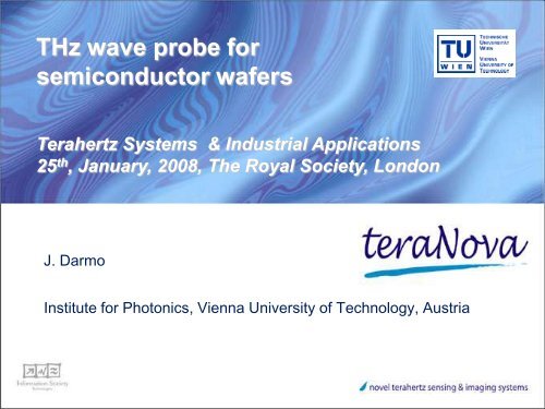
THz wave probe for<br />
semiconductor wafers<br />
Terahertz Systems & Industrial Applications<br />
25 th , January, 2008, The Royal Society, London<br />
J. Darmo<br />
Institute for Photonics, Vienna University of <strong>Technology</strong>, Austria
Talk outline<br />
• Why THz waves based system<br />
• Principles of operation<br />
• Proof of principle<br />
• Ellipsometry with THz waves<br />
• Interferometry with THz wave (homogeneity mapping)
Why THz based system<br />
Van der Pauw method<br />
THz reflectometry<br />
- sample cleaved from wafer<br />
- good contacts necessary<br />
- direct sampling of wafer
THz-TDS for semiconductor scanner<br />
- conductivity<br />
(doping, mobility)<br />
- carriers’ lifetime<br />
-thickness<br />
(composition)<br />
Remote measurements of carrier<br />
concentration and mobility
Models of relevant structures<br />
THz model of semiconductor<br />
bulk n-type<br />
bulk p-type<br />
n+/n-type<br />
p+/p-type<br />
Drude response<br />
<br />
<br />
<br />
2<br />
<br />
p<br />
<br />
<br />
<br />
Nq<br />
2<br />
<br />
p<br />
2<br />
i<br />
2<br />
1<br />
<br />
m<br />
<br />
p+/n-type<br />
n+/p-type<br />
p/p+/n-type<br />
n/n+/p-type<br />
Mobility model (n-<strong>GaAs</strong>)<br />
<br />
n<br />
p<br />
n<br />
2750 <br />
1<br />
5450<br />
n<br />
0. 54<br />
9.85e16<br />
p 430<br />
0. 45<br />
1<br />
1 <br />
p<br />
6.00 17<br />
<br />
<br />
e
phase shift (rad)<br />
amplitude<br />
attenuation (1/m)<br />
THz model of semiconductor<br />
1.00<br />
0.95<br />
0.90<br />
0.85<br />
0.80<br />
0.75<br />
0.70<br />
0.65<br />
0.60<br />
0.55<br />
0.50<br />
0.45<br />
0.35<br />
0.30<br />
0.25<br />
0.20<br />
0.15<br />
0.10<br />
0.05<br />
0.00<br />
rn_<strong>GaAs</strong><br />
5e15<br />
5e16<br />
5e17<br />
5e18<br />
rn_<strong>GaAs</strong> 1 2 3 4 5 6 7 8<br />
5e16<br />
5e16<br />
frequency 5e17 (THz)<br />
5e18<br />
1 2 3 4 5 6 7 8<br />
frequency (THz)<br />
10<br />
8<br />
6<br />
4<br />
2<br />
0<br />
1.0<br />
0.5<br />
5e17<br />
5e18<br />
5e16<br />
5e17<br />
5e15<br />
0.0<br />
0 1 2 3 4 5 6 7 8<br />
frequency (THz)<br />
Summary:<br />
Multicolour measurement:<br />
un-ambiguous recognition (slow)<br />
Two/three colour measurement:<br />
distinguishable, fast<br />
One colour measurement:<br />
Could be confusing, needs<br />
calibration
Talk outline<br />
• Why THz waves based system<br />
• Principles of operation<br />
• Proof of principle<br />
• Ellipsometry with THz waves<br />
• Interferometry with THz wave (homogeneity mapping)
Targeted parameters<br />
for semiconductorscanner (in 2005)<br />
Semiconductor materials:<br />
<strong>GaAs</strong>, Silicon, InP, GaN<br />
Parameters to access:<br />
conductivity (carrier density & mobility)<br />
(in bulk, epitaxial layer, and 2DEG)<br />
Range of parameters:<br />
typically 10 16 -10 18 cm -3<br />
(range modified to given application)<br />
artistic rendering of scanner<br />
Technicalities:<br />
1. desktop format<br />
2. >10 measurements per minute<br />
3. user/maintenance friendly
Semiconductor scanner hardware<br />
90cm<br />
45cm<br />
40cm<br />
• compact box (90 cm x 40 cm footprint)<br />
• 19“ instrument rack
eflection (arb. units)<br />
reflection (arb. units)<br />
N-<strong>GaAs</strong>: model & experiment<br />
1.1<br />
1.0<br />
0.9<br />
0.8<br />
0.7<br />
3.6um, 4.0um, n=3.80E14 n=5.00E14<br />
4.0um, n=1.38E16 n=1.7E16<br />
2.0um, n=1.00E17 n=1.50E17<br />
2.0um, n=1.55E18 n=1.8E18<br />
0.6<br />
0.5<br />
0.4<br />
0.0 1.0 2.0 3.0 4.0 5.0<br />
frequency [THz]
n-doping (THz data)<br />
Comparison of THz<br />
and standard method<br />
1E19<br />
1E18<br />
N-<strong>GaAs</strong><br />
Thickness: 2-4 m<br />
Substrate: undoped <strong>GaAs</strong><br />
1E17<br />
1E16<br />
1E15<br />
min.<br />
max.<br />
1E14<br />
1E14 1E15 1E16 1E17 1E18 1E19<br />
n-doping (Hall data)<br />
Usable range:<br />
Doping fitting:<br />
1e16 – 5e18 cm -3<br />
Mobility fittting:<br />
1e16 – 5e17 cm -3
mobility (cm 2 /Vs)<br />
mobility (cm 2 /Vs)<br />
<strong>GaAs</strong> & Silicon: model/experiment<br />
8000<br />
doping (cm -3 )<br />
1E15 1E16 1E17 1E18 1E19<br />
10000<br />
<strong>GaAs</strong><br />
<strong>GaAs</strong><br />
deviation from model mobility<br />
observed -> DC vs. HF conductivity<br />
6000<br />
4000<br />
2000<br />
1400<br />
1200<br />
1000<br />
800<br />
600<br />
400<br />
200<br />
0<br />
1E15 1E16 1E17 1E18 1E19<br />
doping (cm -3 )<br />
Silicon<br />
Measurement:<br />
N-doped <strong>GaAs</strong>:<br />
( min : 1800 ->3000 cm 2 /Vs)<br />
N-doped Silicon<br />
( min : 92 ->320 cm 2 /Vs)
HEMT measurement<br />
Heterostructure used:<br />
n+ <strong>GaAs</strong> cap (5 nm)<br />
Al 0.3 Ga 0.7 As (150nm)<br />
undoped <strong>GaAs</strong><br />
undoped <strong>GaAs</strong> substrate
Probing of bulk and 2D carriers<br />
original<br />
THz<br />
in-plane field component<br />
– sheet conductance<br />
normal field component<br />
– optical transitions in QW<br />
2DEG<br />
d
carrier sheet density (THz data)<br />
Summary of the HEMTs measurement<br />
1E12<br />
In<strong>GaAs</strong>/<strong>GaAs</strong><br />
In<strong>GaAs</strong>/InP A<br />
Design of HEMTs:<br />
• <strong>GaAs</strong>/Al<strong>GaAs</strong> (d-doping)<br />
• <strong>GaAs</strong>/In<strong>GaAs</strong> system<br />
• InP/In<strong>GaAs</strong><br />
(single and double doping)<br />
1E11<br />
Al<strong>GaAs</strong>/<strong>GaAs</strong><br />
In<strong>GaAs</strong>/InP B<br />
Conclusions:<br />
• structure model<br />
improvement needed<br />
• calibration works<br />
1E11<br />
1E12<br />
carrier sheet density (Hall data)
Talk outline<br />
• Why THz waves based system<br />
• Principles of operation<br />
• Proof of principle<br />
• Ellipsometry with THz waves<br />
• Interferometry with THz wave (homogeneity mapping)
Ellipsometry & THz waves<br />
p<br />
p<br />
s<br />
s<br />
polarizer<br />
/4 shifter /4 shifter<br />
analyzer<br />
THz ellipsometry:<br />
• wide frequency range available (inherent spectroscopic feature)<br />
• optical components to manipulate polarization of THz needed (!)<br />
• direct evaluation of y and D from FT spectra of E p and E s (standard approach)
Ellipsometry & THz waves<br />
• Electro-optic detector<br />
‣ intrinsic polarization sensitivity<br />
DS<br />
~ cos sin 2<br />
2sin<br />
cos 2<br />
P.C.M. Planken et al., J.Opt.Soc.Am. B313<br />
• THz emitter<br />
‣ electrically controlled (modulated) polarization<br />
~<br />
Phase: linear – circular – elliptical ‘polarization‘<br />
~<br />
Amplitude: ellipticity
Ellipsometry & THz waves<br />
ellipsometric angle D<br />
200<br />
195<br />
190<br />
185<br />
180<br />
175<br />
170<br />
Al<strong>GaAs</strong>/<strong>GaAs</strong><br />
2.90<br />
3.00<br />
3.10<br />
3.20<br />
3.30<br />
ellipsometric angle D<br />
200<br />
195<br />
190<br />
185<br />
180<br />
175<br />
170<br />
Al<strong>GaAs</strong>/<strong>GaAs</strong><br />
=<br />
0.000<br />
0.005<br />
0.010<br />
0.020<br />
165<br />
160<br />
lambda<br />
thickness<br />
0.20 0.25 0.30 0.35 0.40<br />
ellipsometric angle y<br />
Heteroepitaxy case:<br />
• high sensitivity to composition and doping<br />
• high sensitivity to 2DEG presence<br />
(anisotropy)<br />
Homoepitaxy case:<br />
• higher sensitivity for highly doped (strongly<br />
absorbing) layers<br />
ellipsometric angle D<br />
165<br />
160<br />
185<br />
180<br />
175<br />
0.20 0.25 0.30 0.35 0.40<br />
plain <strong>GaAs</strong><br />
ellipsometric angle y<br />
<strong>GaAs</strong>/<strong>GaAs</strong><br />
=<br />
0.05<br />
0.01<br />
0.02<br />
170<br />
0.30 0.35 0.40<br />
ellipsometric angle y
carrier density (10 18 /cm 3 )<br />
Ellipsometry demonstration<br />
3.0<br />
2.5<br />
2.0<br />
1.5<br />
standard THz-TDS<br />
THz ellipsometry<br />
- tests on epitaxial layers (n-<strong>GaAs</strong>)<br />
- tests on heterostructure samples<br />
(2DEG) pHEMT (In<strong>GaAs</strong>/InP)<br />
Al<strong>GaAs</strong>/<strong>GaAs</strong> (MODFET)<br />
1.0<br />
0.5<br />
0.5 1.0 1.5 2.0 2.5 3.0 3.5<br />
Hall carrier density (10 18 /cm 3 )
Talk outline<br />
• Why THz waves based system<br />
• Principles of operation<br />
• Proof of principle<br />
• Ellipsometry with THz waves<br />
• Interferometry with THz wave (homogeneity mapping)
eflectivity change (%)<br />
reflectivity change in phase (rad)<br />
THz model of semiconductor<br />
0.6 1% modulation of doping<br />
0.5<br />
0.4<br />
0.3<br />
0.2<br />
0.1<br />
0.0<br />
10 19<br />
10 17 10 18 10 16<br />
0 2 4 6 8<br />
0.10<br />
0.08<br />
0.06<br />
0.04<br />
0.02<br />
0.00<br />
-0.02<br />
-0.04<br />
10% modulation of doping<br />
10 18<br />
10 17<br />
10 16 10 19<br />
0 2 4 6 8<br />
frequency (THz)<br />
frequency (THz)<br />
Accessibility range<br />
n-<strong>GaAs</strong> 1e16 – 5e19<br />
p-<strong>GaAs</strong> 5e16 – 2e19<br />
n-Si 2e16 – 1e19<br />
p-Si 5e16 – 2e19<br />
(layer’s thickness and structure dependent)
THz interferometer<br />
Schematic drawing of setup
Parameters homogeneity map<br />
4x10 11<br />
3x10 11<br />
Al<strong>GaAs</strong>/<strong>GaAs</strong> based 2DEG<br />
map of 2DEG density<br />
scanned area: 16x16 mm<br />
step size: 0.5 mm<br />
2x10 11<br />
4x10 11<br />
3x10 11<br />
2x10 11<br />
Al<strong>GaAs</strong>/<strong>GaAs</strong> based 2DEG<br />
Map of 2DEG density after treatment<br />
(sample subjected to surface oxidation)<br />
Scanner area: 16x16 mm<br />
Step size: 0.25 mm<br />
1x10 11
Lehighton <strong>Electronics</strong>, Inc. (PA)<br />
LEI 1600/1605 – contactless alternative to Hall measurement<br />
( 10 GHz microwave technology)<br />
LEI 1500/1510 – resistivity mapping (Eddy current measurement)<br />
RS300/LEI 88 – sheet resistivity<br />
LEI 1600 LEI 1500 RS 300<br />
LEI 1605 LEI 1510 LEI88
Summary<br />
• semiconductor scanner demonstrator is built and tested on<br />
epitaxial layers<br />
• potential of ellipsometry for THz wave probe evaluated<br />
• spatial mapping of elecrical parameters with THz wave<br />
probe is demontrated
Those who contributed<br />
scanner team<br />
D. Dietze, T. Prikoszowitch,<br />
P. Kelly, and K. Unterrainer<br />
Institute for Photonics, Vienna University of <strong>Technology</strong>, Austria<br />
fs-oscillator with PhC fiber delivery team<br />
T. Le and A. Stingl<br />
Femtolasers Produktions GmbH, Austria