Custom Packaging Design of Microsystem and ... - INTI
Custom Packaging Design of Microsystem and ... - INTI
Custom Packaging Design of Microsystem and ... - INTI

You also want an ePaper? Increase the reach of your titles
YUMPU automatically turns print PDFs into web optimized ePapers that Google loves.
<strong>Custom</strong> <strong>Packaging</strong> <strong>Design</strong> <strong>of</strong> <strong>Microsystem</strong> <strong>and</strong> Microelectronics Devices<br />
Milano, O.; Roberti, M.; Fraigi, L.<br />
National Institute <strong>of</strong> Industrial Technology (<strong>INTI</strong>), Electronics <strong>and</strong> Informatics Centre<br />
Buenos Aires, Argentina<br />
omar@inti.gov.ar<br />
Abstract<br />
The design, fabrication <strong>and</strong> characterization <strong>of</strong> packaging for integrated circuits <strong>and</strong> MEMS are presented. Thick Film <strong>and</strong><br />
Low Temperature Co-Fired Ceramics (LTCC) Technologies were used to obtain the different packages prototypes. The<br />
performances <strong>of</strong> both technologies were compared.<br />
Keywords: <strong>Microsystem</strong>, Microelectronics, <strong>Packaging</strong>, Thick Film, LTCC<br />
Introduction<br />
As it is well known, the integrated circuits (ICs)<br />
packaging allow, besides electrical connexions between<br />
the IC <strong>and</strong> the external world, mechanical protection <strong>and</strong><br />
an adecuated power distribution <strong>and</strong> dissipation.<br />
On the other h<strong>and</strong>, there are not st<strong>and</strong>ard solutions<br />
for MEMS <strong>and</strong> the packages in this case should be done<br />
depending on the specific application <strong>and</strong> environmental<br />
conditions.<br />
In this paper we present some custom packaging<br />
designs <strong>of</strong> ICs, fuel cell <strong>and</strong> RF devices, applying Thick<br />
Film Technology (TFT) <strong>and</strong> Low Temperature Co-Fired<br />
Ceramics (LTCC) [1]. These technologies are suitable to<br />
perform, besides st<strong>and</strong>ard packages for integrated<br />
circuits, appropriate packages for microsystems.<br />
(c)<br />
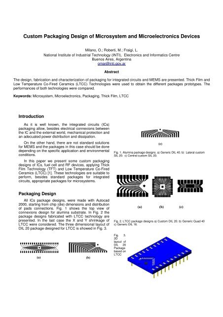
Fig. 1. Alumina package designs. a) Generic DIL 40. b) Lateral custom<br />
SIL 20. c) Central custom SIL 20.<br />
<strong>Packaging</strong> <strong>Design</strong><br />
All ICs package designs, were made with Autocad<br />
2000, starting from chip (die) dimensions <strong>and</strong> distribution<br />
<strong>of</strong> pads connections. Fig. 1 shows the top view <strong>of</strong><br />
connexions design for alumina substrate. In Fig. 2 the<br />
package designs fabricated with LTCC technology are<br />
presented. In the last case the X <strong>and</strong> Y shrinkage <strong>of</strong><br />
LTCC were considered. The three dimensional layout <strong>of</strong><br />
DIL 20 package designed for LTCC is showed in Fig. 3.<br />
(a) (b) (c)<br />
Fig. 2. LTCC package designs a) <strong>Custom</strong> DIL 20. b) Generic Quad 40<br />
c) Generic DIL 16.<br />
(a)<br />
(b)<br />
Fig. 3.<br />
3D<br />
layout <strong>of</strong><br />
DIL 20<br />
Package<br />
based on<br />
LTCC
For the design <strong>of</strong> fuel cell package [2] we choose to design<br />
a functional test bed that can h<strong>and</strong>le fluids, electrical contacts<br />
<strong>and</strong> exchange <strong>of</strong> parts such as: MEA (Membrane Electrode<br />
Assembly) <strong>and</strong> GDL (Gas Diffusion Layer). To accomplish<br />
the exchange <strong>of</strong> MEA <strong>and</strong> GDL, modular structures were<br />
proposed, resulting in comparative tests <strong>of</strong> performance<br />
among the various membranes. In Fig. 4 tree-dimensional<br />
circulation <strong>of</strong> the fluid is showed.<br />
Fig. 5. Detail <strong>of</strong> IC wire bonding.<br />
In Fig. 6. a photography <strong>of</strong> all models <strong>of</strong> thick film <strong>and</strong><br />
LTCC ICs packages is showed.<br />
Fig. 4. Circulation <strong>of</strong> fluid (green - fluid input / blue - fluid in contact to<br />
GDL / red - fluid output)<br />
Fig. 6. Photography <strong>of</strong> alumina <strong>and</strong> LTCC packages.<br />
To the package <strong>of</strong> fuel cell, DuPont 951 LTCC <strong>and</strong><br />
thick film paste 6146 was used. To achieve a modular<br />
cell <strong>and</strong> easy replacement <strong>of</strong> MEA <strong>and</strong> GDL, an<br />
elastomer was used as seal between the structure <strong>of</strong><br />
LTCC <strong>and</strong> membranes. In Fig. 7 a prototype <strong>of</strong> fuel cell<br />
with an elastomer is showed.<br />
For the first RF-Packages prototypes, CPW<br />
(Coplanar Waveguide) lines were designed in order to<br />
adjust the design parameters according to its<br />
characteristic impedance Zo. Three prototype <strong>of</strong> CPW<br />
lines were designed. Two models <strong>of</strong> CPW lines (different<br />
W <strong>and</strong> S) <strong>and</strong> one more to characterize the bonding wire<br />
(WB Model) [3].<br />
Fabrication<br />
Heraeus silver/palladium thick film C1218 was used<br />
as conductor lines for alumina prototypes <strong>of</strong> ICs<br />
packages. St<strong>and</strong>ard thick film process was used.<br />
For LTCC prototype <strong>of</strong> ICs packages, DuPont<br />
Palladium/silver thick film paste 6146 (
solder SMA end launch connectors. Fig. 9 shows<br />
prototype <strong>of</strong> CPW lines with these connectors.<br />
Fig. 9.<br />
Prototy<br />
pe <strong>of</strong><br />
CPW<br />
line<br />
with<br />
SMA<br />
end<br />
launch<br />
connect<br />
ors<br />
TPT HB10 Wire Bonder Machine as mode wedge<br />
was used to WB-Model <strong>of</strong> CPW line [5].<br />
Fig. 11 shows WB model <strong>of</strong> CPW line to analyze the<br />
wire bonding.<br />
ment results<br />
Fig. 11.<br />
WB<br />
model<br />
<strong>of</strong> CPW<br />
line.<br />
(Details<br />
<strong>of</strong><br />
wedge<br />
bonding<br />
wire).<br />
Mea<br />
sure<br />
Fig. 10 shows the equivalent circuit diagram <strong>of</strong> ICs<br />
package traces.<br />
Fig. 10. Equivalent circuit diagram <strong>of</strong> packages traces.<br />
Marconi Instruments Ltd TF 1245A Q-meter was<br />
used in measurement. Capacitance <strong>and</strong> Q factor at<br />
30Mhz were measured. Eq. 1 shows how to calculate<br />
the inductance <strong>of</strong> trace.<br />
Lx=<br />
Eq. 1. Equation <strong>of</strong> trace inductance.<br />
1<br />
w 2 C − L aux<br />
Lx = trace inductance<br />
Laux = auxiliar inductor<br />
w = resonance frequency<br />
C = pattern capacitor<br />
Keithley 4200-SCS characterization system <strong>and</strong><br />
model 590 CV were used to measure trace resistance<br />
<strong>and</strong> capacitance. The values <strong>of</strong> measured capacitances<br />
were in order <strong>of</strong> 10 -15 farad.<br />
In Table I, comparative values <strong>of</strong> electrical<br />
characteristics <strong>of</strong> Central SIL 20 thick film <strong>and</strong> <strong>Custom</strong><br />
DIL 20 LTCC packages are showed.<br />
Central SIL20 TFT Package<br />
<strong>Custom</strong> DIL20 LTCC Package<br />
Pins R[] L[nH] R[] L[nH]<br />
1,20 2,92 176 1,03 18,6<br />
2,19 2,69 171 1,23 18,6<br />
3,18 1,98 165 1,47 22,44<br />
4,17 1,75 154 1,71 22,44<br />
5,16 1,70 149 2,06 26,32<br />
6,15 1,63 14,8 3,19 26,32<br />
7,14 1,51 11 4,01 28,27<br />
8,13 1,48 5,48 4,67 32,21<br />
9,12 1,34 3,64 4,86 34,20<br />
10,11 1,20 3,63 5,10 38,20<br />
Table I. Comparative values <strong>of</strong> electrical characteristics.<br />
In order to characterize the fuel cell prototype, the<br />
properly fluidic circulation, the electrical contacts <strong>and</strong> the<br />
seal were verified according to design specifications [6].<br />
Vector Network Analyzer <strong>of</strong> 40Ghz was used to<br />
characterize CPW lines <strong>and</strong> WB Model. Table II shows<br />
S-Parameters obtained to different models.<br />
f=8Ghz<br />
[db]<br />
Model I Model II WB Model<br />
S11 -17 -20 -15<br />
S12 -1,5 -0,95 -1,46<br />
Table II. S-parameters <strong>of</strong> different CPW lines models.<br />
In table II, we can see great values <strong>of</strong> S12 due to the<br />
resistance <strong>of</strong> the line. This may be improved using<br />
another thick film paste with less resistance by square.<br />
Conclusions<br />
−<br />
−<br />
Thick Film Technology (TFT) <strong>and</strong> Low Temperature<br />
Co-Fired Ceramics (LTCC) Technology is a very<br />
suitable technology to fabricate st<strong>and</strong>ard packages<br />
for ICs <strong>and</strong> custom packages for MEMS.<br />
Electrical characteristics <strong>of</strong> ICs packages fabricated<br />
with both technologies, were compared.
−<br />
−<br />
For the fuel cell prototype, two modules with LTCC<br />
technology were manufactured, one for methanol +<br />
products, another one for O 2 + products. We are<br />
using these modules in order to characterize<br />
commercial MEAs <strong>and</strong> GDLs.<br />
Three models <strong>of</strong> CPW lines applied to RF-MEMS<br />
packaging were fabricated <strong>and</strong> characterized.<br />
References<br />
[1] M. R.Gongora-Rubio, P. Espinoza-Vallejos, L. Sola-Laguna <strong>and</strong> J.<br />
J. Santiago-Aviles; ‘‘Overview <strong>of</strong> Low Temperature Co-Fired Ceramics<br />
Tape Technology for Meso-System Technology’’; Sensors &<br />
Actuators A, Physical; v. 89, 2001, pp. 222 – 241.<br />
[2] R. Dillon, S. Srinivasan, A.S. Aricò, V. Antonucci, “International<br />
activities in DMFC R&D: status <strong>of</strong> technologies <strong>and</strong> potential<br />
applications”; Journal <strong>of</strong> Power Sources 127 (2004) 112–126.<br />
[3] JuHwan Lim, DaeHan Kwon, Jae-Sung Rieh, Soo-Won Kim, <strong>and</strong><br />
SungWoo Hwang, “RF Characterization <strong>and</strong> Modeling <strong>of</strong> Various Wire<br />
Bond Transitions”; IEEE TRANSACTIONS ON ADVANCED<br />
PACKAGING, VOL. 28, NO. 4, NOVEMBER 2005, pp 772 – 778.<br />
[4] M. Góngora-Rubio, M. Roberti, Z.M. da Rocha, L. Fraigi, “LTCC<br />
post load cell”, J. Microelectronics <strong>and</strong> Electronic <strong>Packaging</strong> Vol. 3<br />
(4), 2006, 169-176.<br />
[5] Dean Nicholson <strong>and</strong> HeeSoo Lee, “Characterization <strong>and</strong> modeling<br />
<strong>of</strong> bond wires for high-frequency applications”; Microwave<br />
Engineering Europe, August/September 2006.<br />
[6] Uwe Partsch, Adrian Goldberg, Michael Stelter, “LTCC-Based<br />
Micro-Scale PEM Fuel Cell”; Electronics Systemintegration<br />
Technology Conference, 2006, pp 544 - 549.