Visual System Simulator™
Visual System Simulator™
Visual System Simulator™

You also want an ePaper? Increase the reach of your titles
YUMPU automatically turns print PDFs into web optimized ePapers that Google loves.
<strong>Visual</strong> <strong>System</strong><br />
Simulator <br />
White Paper<br />
AWR’S VISUAL SYSTEM SIMULATOR CO-SIMULATES WITH<br />
NI’S LABVIEW FOR ENHANCED SIGNAL PROCESSING<br />
CAPABILITIES<br />
Achieving the highest possible performance from circuits used in third-and<br />
fourth-generation wireless systems is driving a tighter integration of previously<br />
disparate tools. Certainly, a level of software synergy is essential when<br />
designing circuits for use in today’s wireless systems that employ higher-order<br />
modulation techniques together with advanced technologies, such as Orthogonal<br />
Frequency Division Multiplexing (OFDM), multiple-input multiple-output (MIMO)<br />
and digital predistortion (DPD) circuits, to name a few. As this white paper<br />
illustrates, AWR’s <strong>Visual</strong> <strong>System</strong> Simulator (VSS) and National Instruments’<br />
LabVieW graphical programming environment are now co-simulating so as to<br />
better enable designers to analyze, optimize, and verify complex RF circuits,<br />
subsystems and digital signal processing within a unified framework.<br />
Before looking more closely into specifi c design scenarios, it is important<br />
to understand how this new and cohesive VSS/LabVIEW co-simulation<br />
environment works.<br />
HOW IT WORKS<br />
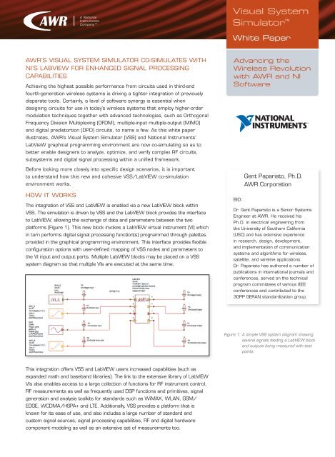
The integration of VSS and LabVIEW is enabled via a new LabVIEW block within<br />
VSS. The simulation is driven by VSS and the LabVIEW block provides the interface<br />
to LabVIEW, allowing the exchange of data and parameters between the two<br />
platforms (Figure 1). This new block invokes a LabVIEW virtual instrument (VI) which<br />
in turn performs digital signal processing function(s) programmed through palettes<br />
provided in the graphical programming environment. This interface provides flexible<br />
configuration options with user-defined mapping of VSS nodes and parameters to<br />
the VI input and output ports. Multiple LabVIEW blocks may be placed on a VSS<br />
system diagram so that multiple VIs are executed at the same time.<br />
Advancing the<br />
Wireless Revolution<br />
with AWR and NI<br />
Software<br />
BIO:<br />
Gent Paparisto, Ph.D.<br />
AWR Corporation<br />
Dr. Gent Paparisto is a Senior <strong>System</strong>s<br />
Engineer at AWR. He received his<br />
Ph.D. in electrical engineering from<br />
the University of Southern California<br />
(USC) and has extensive experience<br />
in research, design, development,<br />
and implementation of communication<br />
systems and algorithms for wireless,<br />
satellite, and wireline applications.<br />
Dr. Paparisto has authored a number of<br />
publications in international journals and<br />
conferences, served on the technical<br />
program committees of various IEEE<br />
conferences and contributed to the<br />
3GPP GERAN standardization group.<br />
Figure 1: A simple VSS system diagram showing<br />
several signals feeding a LabVIEW block<br />
and outputs being measured with test<br />
points.<br />
This integration offers VSS and LabVIEW users increased capabilities (such as<br />
expanded math and baseband libraries). The link to the extensive library of LabVIEW<br />
VIs also enables access to a large collection of functions for RF instrument control,<br />
RF measurements as well as frequently used DSP functions and primitives, signal<br />
generation and analysis toolkits for standards such as WiMAX, WLAN, GSM/<br />
EDGE, WCDMA/HSPA+ and LTE. Additionally, VSS provides a platform that is<br />
known for its ease of use, and also includes a large number of standard and<br />
custom signal sources, signal processing capabilities, RF and digital hardware<br />
component modeling as well as an extensive set of measurements too.
<strong>Visual</strong> <strong>System</strong><br />
Simulator<br />
(additional positioning<br />
line<br />
AXIEM<br />
here ???)<br />
White Paper<br />
There are two options for interfacing with LabVIEW in VSS.<br />
1. Use the LabVIEW Run-Time Engine for executing a VI -- provides<br />
for fast simulation times but disables the creation, modification or<br />
debugging of VIs.<br />
2. Connect to the LabVIEW Development <strong>System</strong> -- provides full flexibility for<br />
creation, modification and debugging of VIs as necessary.<br />
This interface further allows for the use of LabVIEW add-ons and<br />
toolkits, which provide standard signal sources and measurements,<br />
signal processing, analysis and connectivity, integration with<br />
development hardware, and many other capabilities. Taking a<br />
closer look as to how designers may utilize this new co-simulation<br />
environment, the following scenarios are presented.<br />
SCENARIO 1: SIGNAL PROCESSING BLOCKS<br />
VSS can generate signals required for the design and simulation of<br />
modern communication systems. Real, complex, and digital signal<br />
sources can be combined to provide real-world emulation of signals for a<br />
wide range of applications. Figure 2 shows a VSS system diagram with<br />
several of these signals feeding a LabVIEW block (red circle in Figure 2)<br />
and outputs being measured with test points (blue box inset into Figure 2).<br />
The LabVIEW block ties directly to a VI in LabVIEW. The link between VSS<br />
and LabVIEW is managed exclusively by this block. During VSS simulation,<br />
the time-domain data is fed into the LabVIEW data flow and the resulting<br />
VI ouput is resynchronized in time with the VSS simulation. Referring to<br />
Figure 2, the integer data in VSS goes to LabVIEW and its amplitude is<br />
calculated with a summing function and returned to VSS. The resulting<br />
output (Figure 3) - relative to the input - is scaled in amplitude according<br />
to the LabVIEW processing block. The real and complex signals have a<br />
similar operation.<br />
Additionally, LabVIEW VIs can also be used from within the VSS<br />
environment. Consider a simple VI that takes two input signals, adds<br />
them together, and scales the result by a variable gain that is set by a<br />
user-controlled slider (Figure 4). Here, this VI is converted to a “subVI”<br />
by assigning Input 1 and Input 2 numeric controls as input terminals and<br />
Output as an output terminal in the connector pane. This VI can then be<br />
used in a VSS system diagram with a LabVIEW block configured to the<br />
desired VI, and the input and output nodes that will interface with the VI<br />
are added. In essence, the controls and indicators in LabVIEW become<br />
inputs and outputs, respectively, in VSS. This is accomplished by clicking<br />
“Add” under the Input Ports section, selecting the nodes from available<br />
input ports defined in the VI, and if desired defining a name for each port.<br />
The output port is also added and the property propagation is defined.<br />
This simulation also uses the LabVIEW Run-Time Engine and shows<br />
the VI front panel. The input to the VI consists of two tones: 1 and<br />
1.1 GHz. The results are displayed on a graph in the LabVIEW<br />
front panel window, as defi ned in the VI (Figure 5). This window is<br />
automatically opened during the simulation. The results will display<br />
immediately on a VSS graph as well.<br />
Figure 2: The view shows how the LabVIEW block ties directly<br />
to a VI in LabVIEW.<br />
Figure 3: The resulting output relative to the input is scaled in<br />
amplitude according to the LabVIEW processing block.<br />
Figure 4: User-controlled slider within LabVIEW VI.<br />
Figure 5: LabVIEW front panel window displayed within VSS.
<strong>Visual</strong> <strong>System</strong><br />
Simulator<br />
(additional positioning<br />
line<br />
AXIEM<br />
here ???)<br />
White Paper<br />
SCENARIO 2:<br />
A DIGITAL PREDISTORTION (DPD) EXAMPLE<br />
Digital predistortion techniques, employed to overcome the nonlinear<br />
operation of base station amplifiers, have become a mandatory<br />
component to support today’s wider bandwidth signals, high power<br />
efficiency and output linearity requirements. VSS provides an<br />
environment for generating input signals, modeling the circuit-level<br />
amplifier, as well as performing the required measurements. It also<br />
offers the ability to design a DPD proof-of-concept and then convert it<br />
from floating-point to a realistic fixed-point implementation. LabVIEW<br />
includes many of these signal processing capabilities as well but<br />
also offers the option of implementing the resulting design in an<br />
FPGA. In this way, users are greatly aided by the joint VSS/LabVIEW<br />
environment in that it allows for faster design thru to prototype and<br />
test of final DPD implementations.<br />
In this scenario, the predistortion circuit uses digitally-controlled<br />
attenuators and phase shifters and its implementation is moved very<br />
early in the design process to LabVIEW given the new VSS/LabVIEW<br />
unified framework. Based on a circuit-level amplifier, a VI is created<br />
that takes a sample of the signal passing through the amplifier and<br />
creates a predistorted signal. This signal is passed back to VSS where<br />
it enters the amplifier so the resulting signal is more linear. This<br />
process benefits designers in that it provides a seamless methodology<br />
that allows for successively adding more complexity to the circuit while<br />
concurrently evaluating its performance.<br />
Figure 6 shows a 1900 MHz power amplifier from AWR’s library.<br />
The AM/AM and AM/PM curves are shown in Figure 7 along with<br />
the resulting spectrum with QPSK modulation at a power level with<br />
notable distortion (visible as spectral regrowth “side lobes”) simulated<br />
in VSS as a reference. There are two foundational aspects of digital<br />
predistortion that need to be addressed for the technique to work.<br />
A sample of the amplifier’s input-output characteristics must be available<br />
in order to determine what must be corrected. This can be done by<br />
periodically running the digital predistortion circuit in a calibration mode<br />
to characterize the amplifier, or by sampling the amplifier’s output and<br />
building a characterization table dynamically over time.<br />
In this case, the discussion concerns an early stage of the design<br />
process when only the amplifier is being simulated. A copy of the<br />
amplifier can be used to create the characterization dynamically<br />
before the signal reaches the actual amplifier simulation. This is<br />
shown in Figure 8, which is a VSS system diagram in which a copy of<br />
the 1900 MHz amplifier (element S1, circled in Figure 8) is placed<br />
early in the signal path where the signal is predistorted.<br />
The second issue that must be addressed is the amount of correction<br />
required to predistort the signal. While this can be achieved<br />
algorithmically by understanding the AM/AM and AM/PM behavior,<br />
it is being done manually within the VI to illustrate the functionality.<br />
Figure 6: Circuit-level schematic of the1900 MHz<br />
power amplifier.<br />
Figure 7: AM/AM and AM/PM curves from the amplifier along<br />
with the resulting spectrum with QPSK modulation at a<br />
nominal power level simulated in VSS as a reference.<br />
Figure 8: A VSS system diagram of the 1900 MHz amplifier<br />
when placed early in the signal path where the signal is<br />
predistorted.
<strong>Visual</strong> <strong>System</strong><br />
Simulator<br />
(additional positioning<br />
line<br />
AXIEM<br />
here ???)<br />
White Paper<br />
Here, LabVIEW’s benefits become clear as the design flow moves<br />
toward actual hardware, as the VI can be made more realistic by<br />
adding corrective algorithms and extending this VI to measure the<br />
attenuators, phase shifters, and other components that would<br />
otherwise only be modeled in the VSS system diagram.<br />
One of the benefits of the synergy between VSS and LabVIEW is<br />
in the ability of VSS to capture the simulated 1900 MHz amplifier<br />
and LabVIEW to capture the actual attenuators and phase shifters.<br />
The user can determine when and how to switch from manual to<br />
algorithmic behavior given the challenges and progress of the design<br />
flow. The LabVIEW VI is added to the VSS system diagram to create<br />
the predistorted signal (Figure 9). The VSS input signal is transferred<br />
through the LabVIEW block to the VI and separated into phase and<br />
magnitude. These signals are then used early in the development of<br />
the predistortion circuit to drive a look-up table or simple continuous<br />
algorithm corresponding to the phase and magnitude of the output<br />
signal. Operating on the complex signal (as phase and magnitude)<br />
allows direct implementation of the phase shifter and attenuator. As<br />
the digital phase shifter and attenuator are digitally controlled, the<br />
look-up table can be implemented in an FPGA for easy recalibration<br />
or updating as determined by system performance.<br />
First-pass predistorter results are shown in Figure 10. The blue<br />
trace shows the signal as it would appear without predistortion,<br />
while the red trace shows an early manual correction using the<br />
LabVIEW VI to alter the phase and magnitude as a predistortion<br />
function. The improvement is seen in the spectral mask, where<br />
regrowth is reduced by about 25 dB. As the amplifier is driven<br />
harder, the performance should be even more pronounced thereby<br />
maintaining the linearity of the amplifier at higher power levels.<br />
SUMMARY<br />
Achieving the highest possible performance from circuits used<br />
in third-and fourth-generation wireless systems requires the<br />
seamless integration of simulation and measurement at every<br />
stage of the design process. Designers who deviate from this are<br />
at risk as the further in the design process that serious design<br />
issues are discovered, the more time (and money) it will take to<br />
remedy them. AWR’s VSS software and National Instruments’<br />
LabVIEW signifi cantly reduce the possibility that the latter scenario<br />
will occur, as the circuit and its components are passed back<br />
and forth seamlessly between the two tools. The result is better<br />
performance, shorter design time, and a minimum of frustration.<br />
Figure 9: A LabVIEW VI added to the VSS system diagram to create<br />
the predistorted signal.<br />
Figure 10: First-pass predistorter results. The blue trace shows the<br />
signal as it would appear without predistortion, while the red<br />
trace shows an early manual correction using the LabVIEW<br />
VI to alter the phase and magnitude as a predistortion<br />
function. The improvement is seen in the spectral mask,<br />
where regrowth is reduced by about 25 dB.<br />
View the AWR<br />
VSS/LabVIEW<br />
Integration video<br />
on AWR.TV.<br />
AWR, 1960 East Grand Avenue, Suite 430, El Segundo, CA 90245, USA<br />
Tel: +1 (310) 726-3000 Fax: +1 (310) 726-3005 www.awrcorp.com<br />
Copyright © 2012 AWR Corp. All rights reserved. AWR is a National Instruments Company. AWR, and the<br />
AWR logo are registered trademarks and <strong>Visual</strong> <strong>System</strong> Simulator is a trademark of AWR Corporation.<br />
All others are trademarks of their respective holders.<br />
WP-VSS-NI-2012.5.31