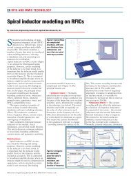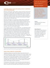
Visual System Simulator™
Visual System Simulator™
Visual System Simulator™

You also want an ePaper? Increase the reach of your titles
YUMPU automatically turns print PDFs into web optimized ePapers that Google loves.
<strong>Visual</strong> <strong>System</strong><br />
Simulator<br />
(additional positioning<br />
line<br />
AXIEM<br />
here ???)<br />
White Paper<br />
SCENARIO 2:<br />
A DIGITAL PREDISTORTION (DPD) EXAMPLE<br />
Digital predistortion techniques, employed to overcome the nonlinear<br />
operation of base station amplifiers, have become a mandatory<br />
component to support today’s wider bandwidth signals, high power<br />
efficiency and output linearity requirements. VSS provides an<br />
environment for generating input signals, modeling the circuit-level<br />
amplifier, as well as performing the required measurements. It also<br />
offers the ability to design a DPD proof-of-concept and then convert it<br />
from floating-point to a realistic fixed-point implementation. LabVIEW<br />
includes many of these signal processing capabilities as well but<br />
also offers the option of implementing the resulting design in an<br />
FPGA. In this way, users are greatly aided by the joint VSS/LabVIEW<br />
environment in that it allows for faster design thru to prototype and<br />
test of final DPD implementations.<br />
In this scenario, the predistortion circuit uses digitally-controlled<br />
attenuators and phase shifters and its implementation is moved very<br />
early in the design process to LabVIEW given the new VSS/LabVIEW<br />
unified framework. Based on a circuit-level amplifier, a VI is created<br />
that takes a sample of the signal passing through the amplifier and<br />
creates a predistorted signal. This signal is passed back to VSS where<br />
it enters the amplifier so the resulting signal is more linear. This<br />
process benefits designers in that it provides a seamless methodology<br />
that allows for successively adding more complexity to the circuit while<br />
concurrently evaluating its performance.<br />
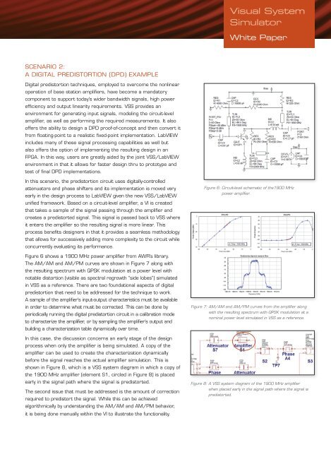
Figure 6 shows a 1900 MHz power amplifier from AWR’s library.<br />
The AM/AM and AM/PM curves are shown in Figure 7 along with<br />
the resulting spectrum with QPSK modulation at a power level with<br />
notable distortion (visible as spectral regrowth “side lobes”) simulated<br />
in VSS as a reference. There are two foundational aspects of digital<br />
predistortion that need to be addressed for the technique to work.<br />
A sample of the amplifier’s input-output characteristics must be available<br />
in order to determine what must be corrected. This can be done by<br />
periodically running the digital predistortion circuit in a calibration mode<br />
to characterize the amplifier, or by sampling the amplifier’s output and<br />
building a characterization table dynamically over time.<br />
In this case, the discussion concerns an early stage of the design<br />
process when only the amplifier is being simulated. A copy of the<br />
amplifier can be used to create the characterization dynamically<br />
before the signal reaches the actual amplifier simulation. This is<br />
shown in Figure 8, which is a VSS system diagram in which a copy of<br />
the 1900 MHz amplifier (element S1, circled in Figure 8) is placed<br />
early in the signal path where the signal is predistorted.<br />
The second issue that must be addressed is the amount of correction<br />
required to predistort the signal. While this can be achieved<br />
algorithmically by understanding the AM/AM and AM/PM behavior,<br />
it is being done manually within the VI to illustrate the functionality.<br />
Figure 6: Circuit-level schematic of the1900 MHz<br />
power amplifier.<br />
Figure 7: AM/AM and AM/PM curves from the amplifier along<br />
with the resulting spectrum with QPSK modulation at a<br />
nominal power level simulated in VSS as a reference.<br />
Figure 8: A VSS system diagram of the 1900 MHz amplifier<br />
when placed early in the signal path where the signal is<br />
predistorted.