CMOS Linear Applications
CMOS Linear Applications
CMOS Linear Applications

You also want an ePaper? Increase the reach of your titles
YUMPU automatically turns print PDFs into web optimized ePapers that Google loves.
<strong>CMOS</strong> <strong>Linear</strong> <strong>Applications</strong><br />
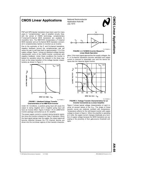
PNP and NPN bipolar transistors have been used for many<br />
years in ‘‘complementary’’ type of amplifier circuits Now<br />
with the arrival of <strong>CMOS</strong> technology complementary<br />
P-channelN-channel MOS transistors are available in<br />
monolithic form The MM74C04 incorporates a P-channel<br />
MOS transistor and an N-channel MOS transistor connected<br />
in complementary fashion to function as an inverter<br />
Due to the symmetry of the P- and N-channel transistors<br />
negative feedback around the complementary pair will<br />
cause the pair to self bias itself to approximately 12 of the<br />
supply voltage Figure 1 shows an idealized voltage transfer<br />
characteristic curve of the <strong>CMOS</strong> inverter connected with<br />
negative feedback Under these conditions the inverter is<br />
biased for operation about the midpoint in the linear segment<br />
on the steep transition of the voltage transfer characteristics<br />
as shown in Figure 1<br />
TLF6020–1<br />
FIGURE 1 Idealized Voltage Transfer<br />
Characteristics of an MM74C04 Inverter<br />
Under AC Conditions a positive going input will cause the<br />
output to swing negative and a negative going input will<br />
have an inverse effect Figure 2 shows 16 of a MM74C04<br />
inverter package connected as an AC amplifier<br />
The power supply current is constant during dynamic operation<br />
since the inverter is biased for Class A operation When<br />
the input signal swings near the supply the output signal will<br />
become distorted because the P-N channel devices are<br />
driven into the non-linear regions of their transfer character-<br />
National Semiconductor<br />
Application Note 88<br />
July 1973<br />
TLF6020–2<br />
FIGURE 2 A 74<strong>CMOS</strong> Inverter Biased for<br />
<strong>Linear</strong> Mode Operation<br />
istics If the input signal approaches the supply voltages the<br />
P- or N-channel transistors become saturated and supply<br />
current is reduced to essentially zero and the device behaves<br />
like the classical digital inverter<br />
TLF6020–3<br />
FIGURE 3 Voltage Transfer Characteristics for an<br />
Inverter Connected as a <strong>Linear</strong> Amplifier<br />
Figure 3 shows typical voltage characteristics of each inverter<br />
at several values of the V CC The shape of these<br />
transfer curves are relatively constant with temperature<br />
Temperature affects for the self-biased inverter with supply<br />
voltage is shown in Figure 4 When the amplifier is operating<br />
at 3 volts the supply current changes drastically as a function<br />
of supply voltage because the MOS transistors are operating<br />
in the proximity of their gate-source threshold voltages<br />
<strong>CMOS</strong> <strong>Linear</strong> <strong>Applications</strong> AN-88<br />
C1995 National Semiconductor Corporation<br />
TLF6020<br />
RRD-B30M105Printed in U S A
Post Amplifier for Op Amps<br />
A standard operational amplifier used with a <strong>CMOS</strong> inverter<br />
for a Post Amplifier has several advantages The operational<br />
amplifier essentially sees no load condition since the input<br />
impedance to the inverter is very high Secondly the<br />
<strong>CMOS</strong> inverters will swing to within millivolts of either supply<br />
This gives the designer the advantage of operating the<br />
operational amplifier under no load conditions yet having<br />
the full supply swing capability on the output Shown in Figure<br />
7 is the LM4250 micropower Op Amp used with a 74C04<br />
inverter for increased output capability while maintaining the<br />
low power advantage of both devices<br />
TLF6020–4<br />
FIGURE 4 Normalized Amplifier Supply Current<br />
Versus Ambient Temperature Characteristics<br />
Figure 5 shows typical curves of voltage gain as a function<br />
of operating frequency for various supply voltages<br />
Output voltages can swing within millivolts of the supplies<br />
with either a single or a dual supply<br />
TLF6020–7<br />
P D e 500 nW<br />
FIGURE 7 MM74C04 Inverter Used as a Post<br />
Amplifier for a Battery Operated Op Amp<br />
The MM74C04 can also be used with single supply amplifier<br />
such as the LM324 With the circuit shown in Figure 8 the<br />
open loop gain is approximately 160 dB The LM324 has 4<br />
amplifiers in a package and the MM74C04 has 6 amplifiers<br />
per package<br />
TLF6020–5<br />
FIGURE 5 Typical Voltage Gain Versus Frequency<br />
Characteristics for Amplifier Shown in Figure 2<br />
APPLICATIONS<br />
Cascading Amplifiers for Higher Gain<br />
By cascading the basic amplifier block shown in Figure 2 a<br />
high gain amplifier can be achieved The gain will be multiplied<br />
by the number of stages used If more than one inverter<br />
is used inside the feedback loop (as in Figure 6) a higher<br />
open loop gain is achieved which results in more accurate<br />
closed loop gains<br />
FIGURE 6 Three <strong>CMOS</strong> Inverters<br />
Used as an X10 AC Amplifier<br />
TLF6020–6<br />
TLF6020–8<br />
FIGURE 8 Single Supply Amplifier Using a <strong>CMOS</strong><br />
Cascade Post Amplifier with the LM324<br />
<strong>CMOS</strong> inverters can be paralleled for increased power to<br />
drive higher current loads Loads of 50 mA per inverter can<br />
be expected under AC conditions<br />
Other 74C devices can be used to provide greater complementary<br />
current outputs The MM74C00 NAND Gate will<br />
provide approximately 10 mA from the V CC supply while the<br />
2
MM74C02 will supply approximately 10 mA from the negative<br />
supply Shown in Figure 9 is an operational amplifier<br />
using a <strong>CMOS</strong> power post amplifier to provide greater than<br />
40 mA complementary currents<br />
Phase Shift Oscillator Using MM74C04<br />
f e 1<br />
33 RC<br />
TLF6020–10<br />
Integrator Using Any Inverting <strong>CMOS</strong> Gate<br />
T e RC<br />
TLF6020–11<br />
Square Wave Oscillator<br />
I OUT 50 mA<br />
V OUT 60 V PP<br />
TLF6020–9<br />
FIGURE 9 MM74C00 and MM74C02 Used as a Post<br />
Amplifier to Provide Increased Current Drive<br />
Other <strong>Applications</strong><br />
Shown in Figure 10 is a variety of applications utilizing<br />
<strong>CMOS</strong> devices Shown is a linear phase shift oscillator and<br />
an integrator which use the <strong>CMOS</strong> devices in the linear<br />
mode as well as a few circuit ideas for clocks and one<br />
shots<br />
Conclusion<br />
Careful study of <strong>CMOS</strong> characteristics show that <strong>CMOS</strong> devices<br />
used in a system design can be used for linear building<br />
blocks as well as digital blocks<br />
Utilization of these new devices will decrease package<br />
count and reduce supply requirements The circuit designer<br />
now can do both digital and linear designs with the same<br />
type of device<br />
One Shot<br />
f e 1<br />
14 RC<br />
TLF6020–12<br />
T e 14 RC<br />
TLF6020–13<br />
Staircase Generator<br />
TLF6020–14<br />
FIGURE 10 Variety of Circuit Ideas<br />
Using <strong>CMOS</strong> Devices<br />
3
AN-88 <strong>CMOS</strong> <strong>Linear</strong> <strong>Applications</strong><br />
LIFE SUPPORT POLICY<br />
NATIONAL’S PRODUCTS ARE NOT AUTHORIZED FOR USE AS CRITICAL COMPONENTS IN LIFE SUPPORT<br />
DEVICES OR SYSTEMS WITHOUT THE EXPRESS WRITTEN APPROVAL OF THE PRESIDENT OF NATIONAL<br />
SEMICONDUCTOR CORPORATION As used herein<br />
1 Life support devices or systems are devices or 2 A critical component is any component of a life<br />
systems which (a) are intended for surgical implant support device or system whose failure to perform can<br />
into the body or (b) support or sustain life and whose be reasonably expected to cause the failure of the life<br />
failure to perform when properly used in accordance support device or system or to affect its safety or<br />
with instructions for use provided in the labeling can effectiveness<br />
be reasonably expected to result in a significant injury<br />
to the user<br />
National Semiconductor National Semiconductor National Semiconductor National Semiconductor<br />
Corporation Europe Hong Kong Ltd Japan Ltd<br />
1111 West Bardin Road Fax (a49) 0-180-530 85 86 13th Floor Straight Block Tel 81-043-299-2309<br />
Arlington TX 76017 Email cnjwge tevm2nsccom Ocean Centre 5 Canton Rd Fax 81-043-299-2408<br />
Tel 1(800) 272-9959 Deutsch Tel (a49) 0-180-530 85 85 Tsimshatsui Kowloon<br />
Fax 1(800) 737-7018 English Tel (a49) 0-180-532 78 32 Hong Kong<br />
Franais Tel (a49) 0-180-532 93 58 Tel (852) 2737-1600<br />
Italiano Tel (a49) 0-180-534 16 80 Fax (852) 2736-9960<br />
National does not assume any responsibility for use of any circuitry described no circuit patent licenses are implied and National reserves the right at any time without notice to change said circuitry and specifications