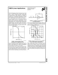
MAX192 Low-Power, 8-Channel, Serial 10-Bit ADC - Robotics UWA
MAX192 Low-Power, 8-Channel, Serial 10-Bit ADC - Robotics UWA
MAX192 Low-Power, 8-Channel, Serial 10-Bit ADC - Robotics UWA

You also want an ePaper? Increase the reach of your titles
YUMPU automatically turns print PDFs into web optimized ePapers that Google loves.
19-0247; Rev. 0; 3/94_______________General DescriptionThe <strong>MAX192</strong> is a low-cost, <strong>10</strong>-bit data-acquisition systemthat combines an 8-channel multiplexer, high-bandwidthtrack/hold, and serial interface with high conversionspeed and ultra-low power consumption. The deviceoperates with a single +5V supply. The analog inputsare software configurable for single-ended and differential(unipolar/bipolar) operation.The 4-wire serial interface connects directly to SPI,QSPI, and Microwire devices, without using externallogic. A serial strobe output allows direct connection toTMS320 family digital signal processors. The <strong>MAX192</strong>uses either the internal clock or an external serial-interfaceclock to perform successive approximation A/Dconversions. The serial interface can operate beyond4MHz when the internal clock is used. The <strong>MAX192</strong> hasan internal 4.096V reference with a drift of ±30ppm typical.A reference-buffer amplifier simplifies gain trim andtwo sub-LSBs reduce quantization errors.The <strong>MAX192</strong> provides a hardwired – S — H D — N – pin and twosoftware-selectable power-down modes. Accessingthe serial interface automatically powers up the device,and the quick turn-on time allows the <strong>MAX192</strong> to beshut down between conversions. By powering downbetween conversions, supply current can be cut tounder <strong>10</strong>µA at reduced sampling rates.The <strong>MAX192</strong> is available in 20-pin DIP and SO packages,and in a shrink-small-outline package (SSOP)that occupies 30% less area than an 8-pin DIP. Thedata format provides hardware and software compatibilitywith the MAX186/MAX188. For anti-aliasing filters,consult the data sheets for the MAX291–MAX297.________________________ApplicationsAutomotivePen-Entry SystemsConsumer ElectronicsPortable Data Logging<strong>Robotics</strong>Battery-<strong>Power</strong>ed Instruments, BatteryManagementMedical Instruments<strong>Low</strong>-<strong>Power</strong>, 8-<strong>Channel</strong>,<strong>Serial</strong> <strong>10</strong>-<strong>Bit</strong> <strong>ADC</strong>____________________________Features♦ 8-<strong>Channel</strong> Single-Ended or 4-<strong>Channel</strong> DifferentialInputs♦ Single +5V Operation♦ <strong>Low</strong> <strong>Power</strong>: 1.5mA (operating)2µA (power-down)♦ Internal Track/Hold, 133kHz Sampling Rate♦ Internal 4.096V Reference♦ 4-Wire <strong>Serial</strong> Interface is Compatiblewith SPI, QSPI, Microwire, and TMS320♦ 20-Pin DIP, SO, SSOP Packages♦ Pin-Compatible 12-<strong>Bit</strong> Upgrade (MAX186/MAX188)______________Ordering InformationPART<strong>MAX192</strong>ACPP<strong>MAX192</strong>BCPPTOP VIEWTEMP. RANGE0°C to +70°C0°C to +70°CPIN-PACKAGE20 Plastic DIP20 Plastic DIP<strong>MAX192</strong>ACWP 0°C to +70°C 20 Wide SO<strong>MAX192</strong>BCWP 0°C to +70°C 20 Wide SO<strong>MAX192</strong>ACAP 0°C to +70°C 20 SSOP<strong>MAX192</strong>BCAP 0°C to +70°C 20 SSOPCH0CH1CH2CH3CH4CH51 23456<strong>MAX192</strong>201918171615V DDSCLKCSDINSSTRBDOUTINL(LSBs)±1/2±1/2±1±1/2±1<strong>MAX192</strong>AEPP -40°C to +85°C 20 Plastic DIP ±1/2<strong>MAX192</strong>BEPP -40°C to +85°C 20 Plastic DIP ±1<strong>MAX192</strong>AEWP -40°C to +85°C 20 Wide SO ±1/2<strong>MAX192</strong>BEWP -40°C to +85°C 20 Wide SO ±1<strong>MAX192</strong>AEAP -40°C to +85°C 20 SSOP ±1/2<strong>MAX192</strong>BEAP -40°C to +85°C 20 SSOP ±1<strong>MAX192</strong>AMJP -55°C to +125°C 20 CERDIP ±1/2<strong>MAX192</strong>BMJP -55°C to +125°C 20 CERDIP ±1__________________Pin Configuration±1<strong>MAX192</strong>CH6714DGNDCH7813AGNDSee last page for Typical Operating Circuit. SPI and QSPI are trademarks of Motorola Corp.Microwire is a trademark of National Semiconductor Corp.AGND 9SHDN <strong>10</strong>DIP/SO/SSOP1211REFADJVREF________________________________________________________________ Maxim Integrated Products 1Call toll free 1-800-998-8800 for free samples or literature.
<strong>Low</strong>-<strong>Power</strong>, 8-<strong>Channel</strong>,<strong>Serial</strong> <strong>10</strong>-<strong>Bit</strong> <strong>ADC</strong>ELECTRICAL CHARACTERISTICS (continued)(V DD = 5V ±5%, f CLK = 2.0MHz, external clock (50% duty cycle), 15 clocks/conversion cycle (133ksps), 4.7µF capacitor at VREF pin,T A = T MIN to T MAX, unless otherwise noted. Typical values are at T A = +25°C.)PARAMETER SYMBOLCONDITIONSMIN TYP MAX UNITSExternal Clock FrequencyExternal compensation, 4.7µFInternal compensation (Note 5)0.<strong>10</strong>.12.00.4 MHzCommon-mode range (any input) (Note 6) 0 V DDUsed for data transfer only<strong>10</strong>ANALOG INPUTSingle-ended range (unipolar only)0 V REFAnalog Input Voltage Unipolar0 V REF VDifferential rangeBipolar- V ––2 R –— E F –+ V ––2 – R — E F –<strong>MAX192</strong>Multiplexer Leakage CurrentOn/off leakage current, V IN = 0V, 5V±0.01 ±1Input Capacitance(Note 5)16INTERNAL REFERENCE (reference buffer enabled)VREF Output VoltageT A = +25°C4.076 4.096 4.116VREF Short-Circuit Current30VREF Tempco±30Load Regulation (Note 7)0mA to 0.5mA output load2.5Capacitive Bypass at VREFInternal compensation0External compensation 4.7Capacitive Bypass at REFADJInternal compensation 0.01External compensation 0.01REFADJ Adjustment Range ±1.5 %EXTERNAL REFERENCE AT VREF (buffer disabled, VREF = 4.096V)µApFVmAppm/°CmVVInput Voltage Range 2.5DD +V50mVInput Current 200 350 µAInput Resistance 12 20 kΩShutdown VREF Input Current 1.5 <strong>10</strong> µABuffer Disable ThresholdREFADJV DD -50mVEXTERNAL REFERENCE AT REFADJCapacitive Bypass at VREFInternal compensation mode 0External compensation mode 4.7µFReference-Buffer Gain 1.678 V/VREFADJ Input Current ±50 µAµFµFV_______________________________________________________________________________________ 3
<strong>Low</strong>-<strong>Power</strong>, 8-<strong>Channel</strong>,<strong>Serial</strong> <strong>10</strong>-<strong>Bit</strong> <strong>ADC</strong><strong>MAX192</strong>ELECTRICAL CHARACTERISTICS (continued)(V DD = 5V ±5%, f CLK = 2.0MHz, external clock (50% duty cycle), 15 clocks/conversion cycle (133ksps), 4.7µF capacitor at VREF pin,T A = T MIN to T MAX, unless otherwise noted. Typical values are at T A = +25°C.)PARAMETER SYMBOLEXTERNAL DIGITAL INPUTS REFERENCE (DIN, SCLK, AT REFADJC — S – , – S — H D — N – )DIN,SCLK, – C — S – Input High Voltage V INHDIN,SCLK, – C — S – Input <strong>Low</strong> Voltage V INLDIN, SCLK, – C — S – Input Hysteresis V HYSTDIN, SCLK, – C — S – Input Leakage I INDIN,SCLK, – C — S – Input Capacitance C IN–S — H D — N – Input High Voltage V INHS — H D — N – Input <strong>Low</strong> VoltageV INLS — H D — N – Input Current, High I INHS — H D — N – Input Current, <strong>Low</strong>I INL–S — H D — N – Input Mid VoltageV IMV FLTS — H D — N – Voltage, Floating–S — H D — N – Max Allowed Leakage,Mid InputDIGITAL OUTPUTS (DOUT, SSTRB)Output Voltage <strong>Low</strong>V OLV IN = 0V or V DDCONDITIONS(Note 5)–S — H D — N – = V DD–S — H D — N – = 0VS — H — D — N – = open–S — H — D — N – = openI SINK = 5mAI SINK = 16mAMIN TYP MAX2.40.80.15±115V DD - 0.50.54.0-4.01.5 V DD - 1.52.75-<strong>10</strong>0 <strong>10</strong>0Output Voltage High V OH I SOURCE = 1mA 4 VThree-State Leakage Current I L C — S – = 5V ±<strong>10</strong> µAThree-State Leakage Capacitance C OUT– C— S– = 5V (Note 5) 15 pFPOWER REQUIREMENTSPositive Supply Voltage V DD 5 ±5% V0.30.4UNITSOperating mode 1.5 2.5 mAPositive Supply Current I DD Fast power-down 30 70Full power-down 2 <strong>10</strong>VVVµApFVVµAµAVVnAVµAPositive Supply Rejection(Note 8)PSRV DD = 5V ±5%; external reference, 4.096V;full-scale input±0.06 ±0.5 mVNote 1: Tested at V DD = 5.0V; single-ended, unipolar.Note 2: Relative accuracy is the deviation of the analog value at any code from its theoretical value after the full-scale range hasbeen calibrated.Note 3: Grounded on-channel; sine wave applied to all off channels.Note 4: Conversion time defined as the number of clock cycles times the clock period; clock has 50% duty cycle.Note 5: Guaranteed by design. Not subject to production testing.Note 6: The common-mode range for the analog inputs is from AGND to V DD .Note 7: External load should not change during conversion for specified accuracy.Note 8: Measured at V SUPPLY +5% and V SUPPLY -5% only.4 _______________________________________________________________________________________
<strong>Low</strong>-<strong>Power</strong>, 8-<strong>Channel</strong>,<strong>Serial</strong> <strong>10</strong>-<strong>Bit</strong> <strong>ADC</strong>s<strong>MAX192</strong>_____________________________________________________________Pin DescriptionPIN NAME FUNCTION1–8 CH0–CH7 Sampling Analog Inputs9, 13 AGNDAnalog Ground. Also IN- Input for single-enabled conversions. Connect both AGND pins toanalog ground.<strong>10</strong> S — H D — N – rent, otherwise the <strong>MAX192</strong> is fully operational. Pulling SHDN high puts the reference-buffer amplifierin internal compensation mode. Letting SHDN float puts the reference-buffer amplifier in externalThree-Level Shutdown Input. Pulling SHDN low shuts the <strong>MAX192</strong> down to <strong>10</strong>µA (max) supply cur-compensation mode.11 VREFReference Voltage for analog-to-digital conversion. Also, Output of the Reference Buffer Amplifier.Add a 4.7µF capacitor to ground when using external compensation mode. Also functions as aninput when used with a precision external reference.12 REFADJ Reference-Buffer Amplifier Input. To disable the reference-buffer amplifier, tie REFADJ to V DD.14 DGND Digital Ground15 DOUT<strong>Serial</strong> Data Output. Data is clocked out at the falling edge of SCLK. High impedance when – C — S – ishigh.16 SSTRB<strong>Serial</strong> Strobe Output. In internal clock mode, SSTRB goes low when the <strong>MAX192</strong> begins the A/Dconversion and goes high when the conversion is done. In external clock mode, SSTRB pulseshigh for one clock period before the MSB decision. SSTRB is high impedance when – C — S – is high(external mode).17 DIN <strong>Serial</strong> Data Input. Data is clocked in at the rising edge of SCLK.18 C — S – Active-<strong>Low</strong> Chip Select. Data will not be clocked into DIN unless – C — S – is low. When – C — S – is high,DOUT is high impedance.19 SCLK<strong>Serial</strong> Clock Input. Clocks data in and out of serial interface. In external clock mode, SCLK alsosets the conversion speed. (Duty cycle must be 45% to 55%.)20 V DD Positive Supply Voltage, +5V ±5%+5V+5V3k3kDOUTDOUTDOUTDOUT3kC LO<strong>ADC</strong> LOAD3kC LO<strong>ADC</strong> LOADDGNDDGNDDGNDDGNDa. High-Z to V OH and V OL to V OH b. High-Z to V OL and V OH to V OL a V OH to High-Zb V OL to High-ZFigure 1. Load Circuits for Enable TimeFigure 2. Load Circuits for Disabled Time6 ________________________________________________________________________________________________
<strong>Low</strong>-<strong>Power</strong>, 8-<strong>Channel</strong>,<strong>Serial</strong> <strong>10</strong>-<strong>Bit</strong> <strong>ADC</strong>CSSCLKDINSHDN181917<strong>10</strong>CH01CH1 2CH2 3CH3 4CH4 5CH5 6CH6 7 CH7 8AGND 13AGND 9REFADJ12VREF 11INPUTSHIFTREGISTERANALOGINPUTMUX+2.46VREFERENCECONTROLLOGICT/HINTCLOCKA ≈ 1.6520kCLOCKINSAR<strong>ADC</strong>OUTREF+4.096VOUTPUTSHIFTREGISTER<strong>MAX192</strong>15162014DOUTSSTRBV DDDGNDCH0CH1CH2CH3CH4CH5CH6CH7AGNDVREFINPUTMUXCAPACITIVE DACC HOLD– +16pFC SWITCHTRACKT/HSWITCHZERO<strong>10</strong>kR SHOLDCOMPARATORAT THE SAMPLING INSTANT,THE MUX INPUT SWITCHES FROM THE SELECTED IN+ CHANNEL TO THE SELECTED IN- CHANNEL.SINGLE-ENDED MODE: IN+ = CHO-CH7, IN- = AGND.DIFFERENTIAL MODE (BIPOLAR): IN+ AND IN- SELECTED FROM PAIRS OFCH0/CH1, CH2/CH3, CH4/CH5, CH6/CH7.<strong>MAX192</strong>Figure 3.Block Diagram_______________Detailed DescriptionThe <strong>MAX192</strong> uses a successive-approximation conversiontechnique and input track/hold (T/H) circuitry toconvert an analog signal to a <strong>10</strong>-bit digital output. Aflexible serial interface provides easy interface tomicroprocessors. No external hold capacitors arerequired. Figure 3 shows the block diagram for the<strong>MAX192</strong>.Pseudo-Differential InputThe sampling architecture of the <strong>ADC</strong>’s analog comparatoris illustrated in the Equivalent Input Circuit(Figure 4). In single-ended mode, IN+ is internallyswitched to CH0–CH7 and IN- is switched to AGND. Indifferential mode, IN+ and IN- are selected from pairsof CH0/CH1, CH2/CH3, CH4/CH5 and CH6/CH7. Referto Tables 1 and 2 to configure the channels.In differential mode, IN- and IN+ are internally switchedto either one of the analog inputs. This configuration ispseudo-differential to the effect that only the signal atIN+ is sampled. The return side (IN-) must remain stablewithin ±0.5LSB (±0.1LSB for best results) withFigure 4. Equivalent Input Circuitrespect to AGND during a conversion. Accomplish thisby connecting a 0.1µF capacitor from AIN- (the selectedanalog input, respectively) to AGND.During the acquisition interval, the channel selected asthe positive input (IN+) charges capacitor C HOLD . Theacquisition interval spans three SCLK cycles and endson the falling SCLK edge after the last bit of the inputcontrol word has been entered. At the end of the acquisitioninterval, the T/H switch opens, retaining chargeon CHOLD as a sample of the signal at IN+.The conversion interval begins with the input multiplexerswitching CHOLD from the positive input (IN+) to thenegative input (IN-). In single-ended mode, IN- issimply AGND. This unbalances node ZERO at the inputof the comparator. The capacitive DAC adjusts duringthe remainder of the conversion cycle to restore itsnode ZERO to 0V within the limits of its resolution. Thisaction is equivalent to transferring a charge of16pF x (VIN+ - VIN-) from CHOLD to the binary-weightedcapacitive DAC, which in turn forms a digital representationof the analog input signal._______________________________________________________________________________________ 7
<strong>Low</strong>-<strong>Power</strong>, 8-<strong>Channel</strong>,<strong>Serial</strong> <strong>10</strong>-<strong>Bit</strong> <strong>ADC</strong><strong>MAX192</strong>Track/HoldThe T/H enters its tracking mode on the falling clock edgeafter the fifth bit of the 8-bit control word has been shiftedin. The T/H enters its hold mode on the falling clock edgeafter the eighth bit of the control word has been shifted in.If the converter is set up for single-ended inputs, IN- isconnected to AGND, and the converter samples the “+”input. If the converter is set up for differential inputs, INconnectsto the “-” input, and the difference of |IN+ - IN-|is sampled. At the end of the conversion, the positiveinput connects back to IN+, and C HOLD charges to theinput signal.The time required for the T/H to acquire an input signal isa function of how quickly its input capacitance ischarged. If the input signal’s source impedance is high,the acquisition time lengthens and more time must beallowed between conversions. Acquisition time is calculatedby:t AZ = 9 (R S + R IN ) 16pFwhere R IN = 5kΩ, R S = the source impedance of the inputsignal, and t AZ is never less than 1.5µs. Note that sourceimpedances below 5kΩ do not significantly affect the ACperformance of the <strong>ADC</strong>.Input BandwidthThe <strong>ADC</strong>’s input tracking circuitry has a 4.5MHzsmall-signal bandwidth, so it is possible to digitizehigh-speed transient events and measure periodic signalswith bandwidths exceeding the <strong>ADC</strong>’s sampling rateby using undersampling techniques. To avoid high-frequencysignals being aliased into the frequency band ofinterest, anti-alias filtering is recommended. See the datasheets for the MAX291–MAX297 filters.Table 1. <strong>Channel</strong> Selection in Single-Ended Mode (SGL/DIFF = 1)Analog Input Range and Input ProtectionInternal protection diodes, which clamp the analoginput to V DD and AGND, allow the channel input pins toswing from AGND - 0.3V to V DD + 0.3V without damage.However, for accurate conversions near full scale,the inputs must not exceed V DD by more than 50mV, orbe lower than AGND by 50mV.If an off-channel analog input exceeds the suppliesby more than 50mV, current will flow through theprotection diodes on that input. If this currentexceeds 2mA, the accuracy of the on-channel’s conversionwill be degraded.The <strong>MAX192</strong> can be configured for differential (unipolaror bipolar) or single-ended (unipolar only) inputs, asselected by bits 2 and 3 of the control byte (Table 3).In the single-ended mode, set the UNI/BIP bit to unipolar.In this mode, analog inputs are internally referencedto AGND, with a full-scale input range from 0V to V REF .In differential mode, both unipolar and bipolar settingscan be used. Choosing unipolar mode sets the differentialinput range at 0V to V REF . The output code isinvalid (code zero) when a negative differential inputvoltage is applied. Bipolar mode sets the differentialinput range to ±V REF / 2. Note that in this differentialmode, the common-mode input range includes bothsupply rails. Refer to Tables 4a and 4b for input voltageranges.Quick LookTo evaluate the analog performance of the <strong>MAX192</strong>quickly, use Figure 5’s circuit. The <strong>MAX192</strong> requires acontrol byte to be written to DIN before eachSEL2 SEL1 SEL0 CH0 CH1 CH2 CH3 CH4 CH5 CH6 CH7 AGND0 0 0 + –1 0 0 + –0 0 1 + –1 0 1 + –0 1 0 + –1 1 0 + –0 1 1 + –1 1 1 + –8 _______________________________________________________________________________________
<strong>Low</strong>-<strong>Power</strong>, 8-<strong>Channel</strong>,<strong>Serial</strong> <strong>10</strong>-<strong>Bit</strong> <strong>ADC</strong>Table 2. <strong>Channel</strong> Selection in Differential Mode (SGL/DIFF = 0)SEL2 SEL1 SEL0 CH0 CH1 CH2 CH3 CH4 CH5 CH6 CH70 0 0 + –0 0 1 + –0 1 0 + –0 1 1 + –1 0 0 – +1 0 1 – +1 1 0 – +1 1 1 – +<strong>MAX192</strong>Table 3. Control-Byte Format<strong>Bit</strong> 7 <strong>Bit</strong> 6 <strong>Bit</strong> 5 <strong>Bit</strong> 4 <strong>Bit</strong> 3 <strong>Bit</strong> 2 <strong>Bit</strong> 1 <strong>Bit</strong> 0(MSB)(LSB)START SEL2 SEL1 SEL0 UNI/ – B — I — P – SGL/ – D — I — F – PD1 PD0<strong>Bit</strong> Name Description7(MSB) START The first logic “1” bit after – C — S – goes low defines the beginning of the control byte.6 SEL2 These three bits select which of the eight channels are used for the conversion.5 SEL1 See Tables 1 and 2.4 SEL03 UNI/ B –— I P – 1 = unipolar, 0 = bipolar. Selects unipolar or bipolar conversion mode. In unipolarmode, an analog input signal from 0V to VREF can be converted; in differential bipolarmode, the differential signal can range from -VREF / 2 to +VREF / 2. Select differentialoperation if bipolar mode is used.2 SGL/ – D — I F – 1 = single ended, 0 = differential. Selects single-ended or differential conversions. Insingle-ended mode, input signal voltages are referred to AGND. In differential mode,the voltage difference between two channels is measured. Select unipolar operationif single-ended mode is used. See Tables 1 and 2.1 PD1 Selects clock and power-down modes.0(LSB) PD0 PD1 PD0 Mode0 0 Full power-down (I Q = 2µA)0 1 Fast power-down (I Q = 30µA)1 0 Internal clock mode1 1 External clock mode_______________________________________________________________________________________ 9
<strong>Low</strong>-<strong>Power</strong>, 8-<strong>Channel</strong>,<strong>Serial</strong> <strong>10</strong>-<strong>Bit</strong> <strong>ADC</strong><strong>MAX192</strong>Table 4a. Unipolar Full Scale and Zero ScaleREFERENCEZEROSCALEFULL SCALEInternal Reference 0V +4.096VTable 4b. Differential Bipolar Full Scale, Zero Scale,and Negative Full ScaleREFERENCENEGATIVE ZEROFULL SCALE SCALEFULL SCALEInternal Reference -4.096V / 2 0V +4.096V / 2ExternalReferenceat REFADJat VREF0V0VV REFADJ (1.678)V REFat -1/2V REFADJ+1/2V0VREFADJExternal REFADJ (1.678)(1.678)Referenceat VREF -1/2 V REF 0V +1/2 V REFconversion. Tying DIN to +5V feeds in control bytes of$FF (HEX), which trigger single-ended conversions onCH7 in external clock mode without powering downbetween conversions. In external clock mode, theSSTRB output pulses high for one clock period beforethe most significant bit of the conversion result comesout of DOUT. Varying the analog input to CH7 shouldalter the sequence of bits from DOUT. A total of 15clock cycles is required per conversion. All transitionsof the SSTRB and DOUT outputs occur on the fallingedge of SCLK.How to Start a ConversionA conversion is started on the <strong>MAX192</strong> by clocking acontrol–byte into DIN. Each rising edge on SCLK, withC — S – low, clocks a bit from DIN into the <strong>MAX192</strong>’s internalshift register. After – C — S – falls, the first arriving logic“1” bit defines the MSB of the control byte. Until thisfirst “start” bit arrives, any number of logic “0” bits canbe clocked into DIN with no effect. Table 3 shows thecontrol-byte format.The <strong>MAX192</strong> is compatible with Microwire, SPI, andQSPI devices. For SPI, select the correct clock polarityand sampling edge in the SPI control registers: setCPOL = 0 and CPHA = 0. Microwire and SPI bothtransmit a byte and receive a byte at the same time.Using the Typical Operating Circuit, the simplest softwareinterface requires only three 8-bit transfers to performa conversion (one 8-bit transfer to configure the<strong>ADC</strong>, and two more 8-bit transfers to clock out the12-bit conversion result).Example: Simple Software InterfaceMake sure the CPU’s serial interface runs in mastermode so the CPU generates the serial clock. Choose aclock frequency from <strong>10</strong>0kHz to 2MHz.1) Set up the control byte for external clock mode,call it TB1. TB1 should be of the format:1XXXXX11 binary, where the Xs denote the particularchannel and conversion-mode selected.2) Use a general-purpose I/O line on the CPU topull C –— S – on the <strong>MAX192</strong> low.3) Transmit TB1 and simultaneously receive a byteand call it RB1. Ignore RB1.4) Transmit a byte of all zeros ($00 HEX) andsimultaneously receive byte RB2.5) Transmit a byte of all zeros ($00 HEX) andsimultaneously receive byte RB3.6) Pull C –— S – on the <strong>MAX192</strong> high.Figure 6 shows the timing for this sequence. BytesRB2 and RB3 will contain the result of the conversionpadded with one leading zero, two sub-LSB bits, andthree trailing zeros. The total conversion time is a functionof the serial clock frequency and the amount ofdead time between 8-bit transfers. Make sure that thetotal conversion time does not exceed 120µs, to avoidexcessive T/H droop.Digital OutputIn unipolar input mode, the output is straight binary(Figure 15). For bipolar inputs in differential mode, theoutput is twos-complement (Figure 16). Data is clockedout at the falling edge of SCLK in MSB-first format.Internal and External Clock ModesThe <strong>MAX192</strong> may use either an external serial clock orthe internal clock to perform the successive-approximationconversion. In both clock modes, the external clockshifts data in and out of the <strong>MAX192</strong>. The T/H acquiresthe input signal as the last three bits of the control byteare clocked into DIN. <strong>Bit</strong>s PD1 and PD0 of the controlbyte program the clock mode. Figures 7 through <strong>10</strong>show the timing characteristics common to bothmodes.<strong>10</strong> ______________________________________________________________________________________
<strong>Low</strong>-<strong>Power</strong>, 8-<strong>Channel</strong>,<strong>Serial</strong> <strong>10</strong>-<strong>Bit</strong> <strong>ADC</strong>0V TO4.096VANALOG0.01µFINPUTCH7<strong>MAX192</strong>V DDDGNDAGNDAGNDCSSCLK+5V0.1µFOSCILLOSCOPESCLKSSTRBDOUT*<strong>MAX192</strong>+5VDIN+5V2MHzOSCILLATORCH1 CH2 CH3 CH4D11N4148REFADJDOUTSSTRBC20.01µFC14.7µFVREF+2.5V+2.5VREFERENCE**SHDNN.C.* FULL-SCALE ANALOG INPUT, CONVERSION RESULT = $FFF (HEX)**OPTIONAL. A POTENTIOMETER MAY BE USED IN PLACE OF THE REFERENCE FOR TEST PURPOSES.Figure 5. Quick-Look CircuitExternal ClockIn external clock mode, the external clock not onlyshifts data in and out, it also drives the analog-to-digitalconversion steps. SSTRB pulses high for one clockperiod after the last bit of the control byte.Successive-approximation bit decisions are made andappear at DOUT on each of the next 12 SCLK fallingedges (see Figure 6). The first <strong>10</strong> bits are the true databits, and the last two are sub-LSB bits.SSTRB and DOUT go into a high-impedance state when–C — S – goes high; after the next C –— S – falling edge, SSTRB willoutput a logic low. Figure 8 shows the SSTRB timing inexternal clock mode.The conversion must complete in some minimum time,or else droop on the sample-and-hold capacitors maydegrade conversion results. Use internal clock mode ifthe clock period exceeds <strong>10</strong>µs, or if serial-clock interruptionscould cause the conversion interval to exceed120µs.Internal ClockIn internal clock mode, the <strong>MAX192</strong> generates its ownconversion clock internally. This frees the microprocessorfrom the burden of running the SAR conversionclock, and allows the conversion results to be readback at the processor’s convenience, at any clock ratefrom zero to typically <strong>10</strong>MHz. SSTRB goes low at thestart of the conversion and then goes high when theconversion is complete. SSTRB will be low for a maximumof <strong>10</strong>µs, during which time SCLK should remainlow for best noise performance. An internal registerstores data when the conversion is in progress. SCLKclocks the data out at this register at any time after theconversion is complete. After SSTRB goes high, thenext falling clock edge will produce the MSB of theconversion at DOUT, followed by the remaining bits inMSB-first format (Figure 9). – C — S – does not need to beheld low once a conversion is started.Pulling – C — S – high prevents data from being clocked into______________________________________________________________________________________ 11
t DSt DH<strong>Low</strong>-<strong>Power</strong>, 8-<strong>Channel</strong>,<strong>Serial</strong> <strong>10</strong>-<strong>Bit</strong> <strong>ADC</strong><strong>MAX192</strong>CSSCLKDIN1 4 8 12 16 20 24START SEL2 SEL1 SEL0UNI/BIPt AZRB1 RB2 RB3SSTRBRB2RB3DOUTA/D STATEIDLERB1SCL/DIFF PD1 PD0 B9ACQUISITIONAUTO ZERO1.5µs (CLK = 2MHz)RB2MSB B8 B7 B6 B5 B4 B3 B2 B1CONVERSIONRB3B0FILLED WITH LSB S1 SO ZEROSIDLEFigure 6. 24-<strong>Bit</strong> External Clock Mode Conversion Timing (SPI, QSPI and Microwire Compatible)CS• • •t CSHt CSSt CLt CSHSCLK• • •DIN• • •t DVt CHt DO t TRDOUT• • •Figure 7. Detailed <strong>Serial</strong>-Interface Timingthe <strong>MAX192</strong> and three-states DOUT, but it does notadversely affect an internal clock-mode conversionalready in progress. When internal clock mode isselected, SSTRB does not go into a high-impedancestate when – C — S – goes high.Figure <strong>10</strong> shows the SSTRB timing in internal clockmode. In internal clock mode, data can be shifted inand out of the <strong>MAX192</strong> at clock rates exceeding4.0MHz, provided that the minimum acquisition time,tAZ, is kept above 1.5µs.Data FramingThe falling edge of – C — S – does not start a conversion on the<strong>MAX192</strong>. The first logic high clocked into DIN is interpretedas a start bit and defines the first bit of the controlbyte. A conversion starts on the falling edge of SCLK,after the eighth bit of the control byte (the PD0 bit) isclocked into DIN. The start bit is defined as:The first high bit clocked into DIN with C –— S – low anytimethe converter is idle, e.g. after V DD is applied.ORThe first high bit clocked into DIN after bit 3 of aconversion in progress is clocked onto the DOUT pin.If a falling edge on – C — S – forces a start bit before bit 3(B3) becomes available, then the current conversionwill be terminated and a new one started. Thus, thefastest the <strong>MAX192</strong> can run is 15 clocks per conversion.Figure 11a shows the serial-interface timing necessaryto perform a conversion every 15 SCLK cyclesin external clock mode.12 ______________________________________________________________________________________
<strong>Low</strong>-<strong>Power</strong>, 8-<strong>Channel</strong>,<strong>Serial</strong> <strong>10</strong>-<strong>Bit</strong> <strong>ADC</strong>CSSSTRBt SDV• • •• • • • • •• • •t STR<strong>MAX192</strong>t SSTRBt SSTRBSCLK• • • • • • • •Figure 8. External Clock Mode SSTRB Detailed TimingPD0 CLOCKED INCSSCLK1 2 3 4 5 6 7 8 9 <strong>10</strong> 11 12 18 19 20 21 22 23 24DINSTART SEL2 SEL1 SEL0UNI/DIPSCL/SSTRBDOUTA/D STATEIDLEDIFF PD1 PD0 B9t CONVACQUISITION CONVERSIONAUTO ZERO <strong>10</strong>µs MAX1.5µs (CLK = 2MHz)MSB B8 B7 B0LSB S1 S0IDLEFILLED WITH ZEROSFigure 9. Internal Clock Mode TimingMost microcontrollers require that conversions occur inmultiples of 8 SCLK clocks; 16 clocks per conversionwill typically be the fastest that a microcontroller candrive the <strong>MAX192</strong>. Figure 11b shows the serial-interfacetiming necessary to perform a conversion every 16SCLK cycles in external clock mode.__________ Applications Information<strong>Power</strong>-On ResetWhen power is first applied and if – S — H D — N – is not pulledlow, internal power-on reset circuitry will activate the<strong>MAX192</strong> in internal clock mode, ready to convert withSSTRB = high. After the power supplies have been stabilized,the internal reset time is <strong>10</strong>0µs and no conversionsshould be performed during this phase. SSTRB ishigh on power-up and, if – C — S – is low, the first logical 1 onDIN will be interpreted as a start bit. Until a conversiontakes place, DOUT will shift out zeros.Reference-Buffer CompensationIn addition to its shutdown function, the – S — H D — N – pin alsoselects internal or external compensation. The compensationaffects both power-up time and maximum conversionspeed. Compensated or not, the minimum clockrate is <strong>10</strong>0kHz due to droop on the sample-and-hold.To select external compensation, float – S — H D — N – . See theTypical Operating Circuit, which uses a 4.7µF capacitor atVREF. A value of 4.7µF or greater ensures stability andallows operation of the converter at the full clock speed of2MHz. External compensation increases power-up time(see the Choosing <strong>Power</strong>-Down Mode section, and Table 5).Internal compensation requires no external capacitor atVREF, and is selected by pulling – S — H D — N – high. Internalcompensation allows for shortest power-up times, but is______________________________________________________________________________________ 13
<strong>Low</strong>-<strong>Power</strong>, 8-<strong>Channel</strong>,<strong>Serial</strong> <strong>10</strong>-<strong>Bit</strong> <strong>ADC</strong><strong>MAX192</strong>CSSSTRBt CSHt CONVt SCKt CSSt SSTRBSCLKPD0 CLOCK INNOTE: FOR BEST NOISE PERFORMANCE, KEEP SCLK LOW DURING CONVERSION.Figure <strong>10</strong>. Internal Clock Mode SSTRB Detailed TimingCSSCLK1 8 1 8 1DINS CONTROL BYTE 0 S CONTROL BYTE 1SCONTROL BYTE 2DOUTSSTRBB9 B8 B7 B6 B5 B4 B3 B2 B1 B0 S1 S0CONVERSION RESULT 0B9 B8 B7 B6 B5 B4 B3 B2 B1 B0 S1 S0CONVERSION RESULT 1Figure 11a. External Clock Mode, 15 Clocks/Conversion TimingCSSCLKDINS CONTROL BYTE 0 S CONTROL BYTE 1DOUTB9 B8 B7 B6 B5 B4 B3 B2 B1 B0 S1 S0CONVERSION RESULT 0B9 B8 B7 B6CONVERSION RESULT 1Figure 11b. External Clock Mode, 16 Clocks/Conversion Timing14 ______________________________________________________________________________________
<strong>Low</strong>-<strong>Power</strong>, 8-<strong>Channel</strong>,<strong>Serial</strong> <strong>10</strong>-<strong>Bit</strong> <strong>ADC</strong>CLOCKMODESHDNDININTERNALSETS EXTERNALCLOCK MODEEXTERNALSXXXXX11 SXXXX X 01SETS FASTPOWER-DOWN MODESETS EXTERNALCLOCK MODES XX XXX1 1EXTERNAL<strong>MAX192</strong>DOUTDATA VALID(<strong>10</strong> + 2 DATA BITS)DATA VALID(<strong>10</strong> + 2 DATA BITS)VALID DATA INVALIDMODEPOWERED UPPOWERED UPFASTPOWER-DOWNFULLPOWERDOWNPOWEREDUPFigure 12a.Timing Diagram <strong>Power</strong>-Down Modes, External ClockCLOCKMODESETS INTERNALCLOCK MODEINTERNAL CLOCK MODESETS FULLPOWER-DOWNDINSXXXXX<strong>10</strong> SXX X X X 00S DOUTDATA VALIDDATA VALIDSSTRBCONVERSIONCONVERSIONMODEPOWERED UPFULLPOWER-DOWNPOWEREDUPFigure 12b. Timing Diagram <strong>Power</strong>-Down Modes, Internal Clockonly available using an external clock and reduces themaximum clock rate to 400kHz.<strong>Power</strong>-DownChoosing <strong>Power</strong>-Down ModeYou can save power by placing the converter in alow-current shutdown state between conversions.Select full power-down or fast power-down mode viabits 7 and 8 of the DIN control byte with – S — H D — N – high(see Tables 3 and 6). Pull – S — H D — N – low at any time to shutdown the converter completely. S –— H D — N – overrides bits 7and 8 of DIN word (see Table 7).Full power-down mode turns off all chip functions that drawquiescent current, typically reducing I DD to 2µA.Fast power-down mode turns off all circuitry except thebandgap reference. With the fast power-down mode,the supply current is 30µA. <strong>Power</strong>-up time can be shortenedto 5µs in internal compensation mode.In both software shutdown modes, the serial interfaceremains operational, however, the <strong>ADC</strong> will not convert.Table 5 illustrates how the choice of reference-buffercompensation and power-down mode affects bothpower-up delay and maximum sample rate.______________________________________________________________________________________ 15
<strong>Low</strong>-<strong>Power</strong>, 8-<strong>Channel</strong>,<strong>Serial</strong> <strong>10</strong>-<strong>Bit</strong> <strong>ADC</strong><strong>MAX192</strong>Table 5.Worst-Case <strong>Power</strong>-Up Delay TimesReference Reference- VREF <strong>Power</strong>- <strong>Power</strong>-Up MaximumBuffer Buffer Capacitor Down Delay SamplingCompensation (µF) Mode (sec) Rate (ksps)ModeEnabled Internal Fast 5µ 26Enabled Internal Full 300µ 26Enabled External 4.7 Fast See Figure 14c 133Enabled External 4.7 Full See Figure 14c 133Disabled Fast 2µ 133Disabled Full 2µ 133Table 6. Software Shutdown and Clock ModePD1 PD0 Device Mode1 1 External Clock Mode1 0 Internal Clock Mode0 1 Fast <strong>Power</strong>-Down Mode0 0 Full <strong>Power</strong>-Down ModeIn external compensation mode, the power-up time is20ms with a 4.7µF compensation capacitor when thecapacitor is fully discharged. In fast power-down, youcan eliminate start-up time by using low-leakage capacitorsthat will not discharge more than 1/2LSB while shutdown. In shutdown, the capacitor has to supply the currentinto the reference (1.5µA typ) and the transient currentsat power-up.Figures 12a and 12b illustrate the various power-downsequences in both external and internal clock modes.Software <strong>Power</strong>-DownSoftware power-down is activated using bits PD1 andPD0 of the control byte. As shown in Table 6, PD1 andPD0 also specify the clock mode. When software shutdownis asserted, the <strong>ADC</strong> will continue to operate inthe last specified clock mode until the conversion iscomplete. Then the <strong>ADC</strong> powers down into a low quiescent-currentstate. In internal clock mode, the interfaceremains active and conversion results may beclocked out while the <strong>MAX192</strong> has already entered asoftware power-down.The first logical 1 on DIN will be interpreted as a startbit, and powers up the <strong>MAX192</strong>. Following the start bit,the data input word or control byte also determinesTable 7. Hard-Wired Shutdown andCompensation ModeSHDN Device Reference-BufferState Mode Compensation1 Enabled Internal CompensationFloating Enabled External Compensation0 Full <strong>Power</strong>-Down N/Aclock and power-down modes. For example, if the DINword contains PD1 = 1, then the chip will remain poweredup. If PD1 = 0, a power-down will resume afterone conversion.Hardware <strong>Power</strong>-DownThe – S — H — D — N – pin places the converter into the fullpower-down mode. Unlike with the software shutdownmodes, conversion is not completed. It stops coincidentallywith – S — H D — N – being brought low. There is nopower-up delay if an external reference is used and isnot shut down. The S –— H D — N – pin also selects internal orexternal reference compensation (see Table 7).<strong>Power</strong>-Down SequencingThe <strong>MAX192</strong> auto power-down modes can save considerablepower when operating at less than maximumsample rates. The following discussion illustrates thevarious power-down sequences.<strong>Low</strong>est <strong>Power</strong> at up to 500Conversions/<strong>Channel</strong>/SecondThe following examples illustrate two differentpower-down sequences. Other combinations of clockrates, compensation modes, and power-down modesmay give lowest power consumption in other applications.16 ______________________________________________________________________________________
<strong>Low</strong>-<strong>Power</strong>, 8-<strong>Channel</strong>,<strong>Serial</strong> <strong>10</strong>-<strong>Bit</strong> <strong>ADC</strong>DINREFADJ2ms WAIT(ZEROS)(ZEROS)CH1CH71 0 01 0 1 1 1 1 1 0 0 1 0 1FULLPD FASTPD NOPD FULLPD FASTPD2.5V0VCOMPLETE CONVERSION SEQUENCE<strong>MAX192</strong>VREF4V0Vτ = RC = 20kΩ x C REFADJt BUFFEN ≈ 15µsFigure 13. FULLPD/FASTPD <strong>Power</strong>-Up SequenceFULL POWER-DOWN<strong>10</strong>00AVG. SUPPLY CURRENT (µA)<strong>10</strong>0<strong>10</strong>18 CHANNELS1 CHANNEL2ms FASTPD WAIT400kHz EXTERNAL CLOCKINTERNAL COMPENSATION0 <strong>10</strong>0 200 300 400 500CONVERSIONS PER CHANNEL PER SECONDFigure 14a. Supply Current vs. Sample Rate/Second, FULLPD,400kHz ClockFigure 14a depicts the <strong>MAX192</strong> power consumption forone or eight channel conversions utilizing fullpower-down mode and internal reference compensation.A 0.01µF bypass capacitor at REFADJ forms anRC filter with the internal 20kΩ reference resistor with a0.2ms time constant. To achieve full <strong>10</strong>-bit accuracy,<strong>10</strong> time constants or 2ms are required after power-up.Waiting 2ms in FASTPD mode instead of full power-upwill reduce the power consumption by a factor of <strong>10</strong> ormore. This is achieved by using the sequence shown inFigure 13.<strong>Low</strong>est <strong>Power</strong> at Higher ThroughputsFigure 14b shows the power consumption withexternal-reference compensation in fast power-down,with one and eight channels converted. The external4.7µF compensation requires a 50µs wait afterpower-up, accomplished by 75 idle clocks after a<strong>MAX192</strong>-14AAVG. SUPPLY CURRENT (µA)POWER-UP DELAY (ms)<strong>10</strong>,000<strong>10</strong>00<strong>10</strong>0<strong>10</strong>3.02.52.01.51.00.508 CHANNELSFAST POWER-DOWN1 CHANNEL2MHz EXTERNAL CLOCKEXTERNAL COMPENSATION50µs WAIT4k 8k 12k 16kCONVERSIONS PER CHANNEL PER SECONDFigure 14b. Supply Current vs. Sample Rate/Second, FASTPD,2MHz Clock00.0001 0.001 0.01 0.1 1 <strong>10</strong>TIME IN SHUTDOWN (sec)Figure 14c. Typical <strong>Power</strong>-Up Delay vs. Time in Shutdown<strong>MAX192</strong>-14B______________________________________________________________________________________ 17
<strong>Low</strong>-<strong>Power</strong>, 8-<strong>Channel</strong>,<strong>Serial</strong> <strong>10</strong>-<strong>Bit</strong> <strong>ADC</strong><strong>MAX192</strong>11 . . . 11111 . . . 1<strong>10</strong>11 . . . <strong>10</strong>1OUTPUT CODEFULL-SCALETRANSITION011 . . . 11<strong>10</strong>11 . . . 1<strong>10</strong>000 . . . 0<strong>10</strong>000 . . . 00<strong>10</strong>00 . . . 000111 . . . 111111 . . . 1<strong>10</strong>111 . . . <strong>10</strong>1FS = +4.09621LSB = +4.096<strong>10</strong>24FS = +4.096V1LSB = FS<strong>10</strong>24<strong>10</strong>0 . . . 001<strong>10</strong>0 . . . 00000 . . . 01<strong>10</strong>0 . . . 0<strong>10</strong>00 . . . 00<strong>10</strong>0 . . . 0000 1 2 3FSINPUT VOLTAGE (LSBs)FS - 3/2LSB-FS0V+FS - 1LSBDIFFERENTIAL INPUT VOLTAGE (LSBs)Figure 15. Unipolar Transfer Function, 4.096V = Full Scale Figure 16. Differential Bipolar Transfer Function,±4.096V / 2 = Full Scaledummy conversion. This circuit combines fastmulti-channel conversion with lowest power consumptionpossible. Full power-down mode may provideincreased power savings in applications where the<strong>MAX192</strong> is inactive for long periods of time, but whereintermittent bursts of high-speed conversions arerequired.External and Internal ReferencesThe <strong>MAX192</strong> can be used with an internal or externalreference. Diode D1 shown in the Typical OperatingCircuit ensures correct start-up. Any standard signaldiode can be used. An external reference can eitherbe connected directly at the VREF terminal or at theREFADJ pin.The <strong>MAX192</strong>’s internally trimmed 2.46V reference isbuffered with a gain of 1.678 to scale an external 2.5Vreference at REFADJ to 4.096V at VREF.Internal ReferenceThe full-scale range of the <strong>MAX192</strong> with internal referenceis 4.096V with unipolar inputs, and ±2.048V with differentialbipolar inputs. The internal reference voltage isadjustable to ±1.5% with the Reference-Adjust Circuit ofFigure 17.External ReferenceAn external reference can be placed at either theinput (REFADJ) or the output (VREF) of the internalbuffer amplifier. The REFADJ input impedance istypically 20kΩ. At VREF, the input impedance is aminimum of 12kΩ for DC currents. During conversion,an external reference at VREF must be able to deliverup to 350µA DC load current and have an outputimpedance of <strong>10</strong>Ω or less. If the reference has higheroutput impedance or is noisy, bypass it close to theVREF pin with a 4.7µF capacitor.Using the buffered REFADJ input avoids externalbuffering of the reference. To use the direct VREF input,disable the internal buffer by tying REFADJ to V DD .Transfer Function and Gain AdjustFigure 15 depicts the nominal, unipolar input/output(I/O) transfer function, and Figure 16 shows the differentialbipolar input/output transfer function. Codetransitions occur halfway between successive integerLSB values. Output coding is binary with1LSB = 4.00mV (4.096V / <strong>10</strong>24) for unipolar operationand 1LSB = 4.00mV [(4.096V / 2 - -4.096V / 2)/<strong>10</strong>24]for bipolar operation.18 ______________________________________________________________________________________
<strong>Low</strong>-<strong>Power</strong>, 8-<strong>Channel</strong>,<strong>Serial</strong> <strong>10</strong>-<strong>Bit</strong> <strong>ADC</strong><strong>10</strong>0k+5V5<strong>10</strong>k12<strong>MAX192</strong>REFADJ+5V GNDR* = <strong>10</strong>ΩSUPPLIES<strong>MAX192</strong>24k0.01µFV DDAGNDDGND+5VDGND<strong>MAX192</strong>DIGITALCIRCUITRY* OPTIONALFigure 17.Reference-Adjust CircuitFigure 18. <strong>Power</strong>-Supply Grounding ConnectionFigure 17, the Reference-Adjust Circuit, shows how toadjust the <strong>ADC</strong> gain in applications that use the internalreference. The circuit provides ±1.5% (±15LSBs) ofgain adjustment range.Layout, Grounding, BypassingFor best performance, use printed circuit boards.Wire-wrap boards are not recommended. Board layoutshould ensure that digital and analog signal lines areseparated from each other. Do not run analog and digital(especially clock) lines parallel to one another, ordigital lines underneath the <strong>ADC</strong> package.Figure 18 shows the recommended system groundconnections. A single-point analog ground (“star”ground point) should be established at AGND, separatefrom the logic ground. All other analog groundsand DGND should be connected to this ground. Noother digital system ground should be connected tothis single-point analog ground. The ground return tothe power supply for this ground should be low impedanceand as short as possible for noise-free operation.High-frequency noise in the V DD power supply mayaffect the high-speed comparator in the <strong>ADC</strong>. Bypassthese supplies to the single-point analog ground with0.1µF and 4.7µF bypass capacitors close to the<strong>MAX192</strong>. Minimize capacitor lead lengths for best supply-noiserejection. If the +5V power supply is verynoisy, a <strong>10</strong>Ω resistor can be connected as a lowpassfilter, as shown in Figure 18.High-Speed Digital InterfacingThe <strong>MAX192</strong> can interface with QSPI at high throughputrates using the circuit in Figure 19. This QSPI circuitcan be programmed to do a conversion on each ofthe eight channels. The result is stored in memory withouttaxing the CPU since QSPI incorporates its ownmicro-sequencer.Figure 20 details the code that sets up QSPI forautonomous operation. In external clock mode, the<strong>MAX192</strong> performs a single-ended, unipolar conversionon each of the eight analog input channels. Figure 21shows the timing associated with the assembly code ofFigure 20. The first byte clocked into the <strong>MAX192</strong> is thecontrol byte, which triggers the first conversion on CH0.The last two bytes clocked into the <strong>MAX192</strong> are allzero, and clock out the results of the CH7 conversion.______________________________________________________________________________________ 19
<strong>Low</strong>-<strong>Power</strong>, 8-<strong>Channel</strong>,<strong>Serial</strong> <strong>10</strong>-<strong>Bit</strong> <strong>ADC</strong><strong>MAX192</strong>ANALOG INPUTS1 CH0V 20 DD2 CH13 CH24 CH35 CH4<strong>MAX192</strong>SCLK 19CS 18DIN 17SSTRB 160.1µF4.7µF+5VV DDI , V DDE , V DDSYN , V STBYSCKPCS0 MC68HC16MOSI6CH5DOUT15MISO7CH6DGND148CH7AGND139AGNDREFADJ12<strong>10</strong>SHDNVREF1<strong>10</strong>.1µF+ 4.7µF0.01µFV SSIV SSE* CLOCK CONNECTIONS NOT SHOWNFigure 19. <strong>MAX192</strong> QSPI ConnectionTMS320 to <strong>MAX192</strong> InterfaceFigure 22 shows an application circuit to interface the<strong>MAX192</strong> to the TMS320 in external clock mode. Thetiming diagram for this interface circuit is shown inFigure 23.Use the following steps to initiate a conversion in the<strong>MAX192</strong> and to read the results:1) The TMS320 should be configured with CLKX(transmit clock) as an active-high output clock andCLKR (TMS320 receive clock) as an active-highinput clock. CLKX and CLKR of the TMS320 aretied together with the SCLK input of the <strong>MAX192</strong>.2) The <strong>MAX192</strong> – C — S – is driven low by the XF_ I/O portof the TMS320 to enable data to be clocked intoDIN of the <strong>MAX192</strong>.3) An 8-bit word (1XXXXX11) should be written to the<strong>MAX192</strong> to initiate a conversion and place thedevice into external clock mode. Refer to Table 3to select the proper XXXXX bit values for your specificapplication.4) The SSTRB output of the <strong>MAX192</strong> is monitored viathe FSR input of the TMS320. A falling edge onthe SSTRB output indicates that the conversion isin progress and data is ready to be received fromthe <strong>MAX192</strong>.5) The TMS320 reads in one data bit on each of thenext 16 rising edges of SCLK. These data bitsrepresent the <strong>10</strong>-bit conversion result and twosub-LSBs, followed by four trailing bits, whichshould be ignored.6) Pull – C — S – high to disable the <strong>MAX192</strong> until the nextconversion is initiated.20 ______________________________________________________________________________________
<strong>Low</strong>-<strong>Power</strong>, 8-<strong>Channel</strong>,<strong>Serial</strong> <strong>10</strong>-<strong>Bit</strong> <strong>ADC</strong>* Description :* This is a shell program for using a stand-alone 68HC16 without any external memory. The internal 1K RAM* is put into bank $0F to maintain 68HC11 code compatibility. This program was written with software* provided in the Motorola 68HC16 Evaluation Kit.** Roger J.A. Chen, Applications Engineer* MAXIM Integrated Products* November 20, 1992*******************************************************************************************************************************************************INCLUDE ‘EQUATES.ASM’ ;Equates for common reg addrsINCLUDE ‘ORG00000.ASM’ ;initialize reset vectorINCLUDE ‘ORG00008.ASM’ ;initialize interrupt vectorsORG $0200 ;start program after interrupt vectorsINCLUDE ‘INITSYS.ASM’ ;set EK=F,XK=0,YK=0,ZK=0;set sys clock at 16.78 MHz, COP offINCLUDE ‘INITRAM.ASM’ ;turn on internal SRAM at $<strong>10</strong>000;set stack (SK=1, SP=03FE)MAIN:JSR INITQSPIMAINLOOP:JSR READ192WAIT:LDAA SPSRANDA #$80BEQ WAIT ;wait for QSPI to finishBRA MAINLOOPENDPROGRAM:<strong>MAX192</strong>INITQSPI:;This routine sets up the QSPI microsequencer to operate on its own.;The sequencer will read all eight channels of a <strong>MAX192</strong> each time;it is triggered. The A/D converter results will be left in the;receive data RAM. Each 16 bit receive data RAM location will;have a leading zero, <strong>10</strong> + 2 bits of conversion result and three zeros.;;Receive RAM <strong>Bit</strong>s 15 14 13 12 11 <strong>10</strong> 09 08 07 06 05 04 03 02 01 00;A/D Result 0 MSB LSB 0 0 0***** Initialize the QSPI Registers ******PSHAPSHBLDAA #%0111<strong>10</strong>00STAA QPDR ;idle state for PCS0-3 = highLDAA #%0111<strong>10</strong>11STAA QPAR ;assign port D to be QSPILDAA #%011111<strong>10</strong>STAA QDDR ;only MISO is an inputLDD #$8008STD SPCR0 ;master mode,16 bits/transfer,;CPOL=CPHA=0,1MHz Ser ClockLDD #$0000STD SPCR1 ;set delay between PCS0 and SCK,;set delay between transfersFigure 20. <strong>MAX192</strong> Assembly-Code Listing______________________________________________________________________________________ 21
<strong>Low</strong>-<strong>Power</strong>, 8-<strong>Channel</strong>,<strong>Serial</strong> <strong>10</strong>-<strong>Bit</strong> <strong>ADC</strong><strong>MAX192</strong>LDD #$0800STD SPCR2 ;set ENDQP to $8 for 9 transfers***** Initialize QSPI Command RAM *****LDAA #$80 ;CONT=1,BITSE=0,DT=0,DSCK=0,PCS0=ACTIVESTAA $FD40 ;store first byte in COMMAND RAMLDAA #$C0 ;CONT=1,BITSE=1,DT=0,DSCK=0,PCS0=ACTIVESTAA $FD41STAA $FD42STAA $FD43STAA $FD44STAA $FD45STAA $FD46STAA $FD47LDAA #$40 ;CONT=0,BITSE=1,DT=0,DSCK=0,PCS0=ACTIVESTAA $FD48***** Initialize QSPI Transmit RAM *****LDDLDDLDDLDDLDDLDDLDDLDD#$008F#$00CF#$009F#$00DF#$00AF#$00EF#$00BF#$00FFLDD #$0000PULBPULARTSSTDSTDSTDSTDSTDSTDSTDSTDSTD$FD20$FD22$FD24$FD26$FD28$FD2A$FD2C$FD2E$FD30READ192:;This routine triggers the QSPI microsequencer to autonomously;trigger conversions on all 8 channels of the <strong>MAX192</strong>. Each;conversion result is stored in the receive data RAM.PSHALDAA #$80ORAA SPCR1STAA SPCR1 ;just set SPEPULARTS***** Interrupts/Exceptions *****BDM: BGND;exception vectors point here;and put the user in background debug modeFigure 20. <strong>MAX192</strong> Assembly-Code Listing (continued)22 ______________________________________________________________________________________
<strong>Low</strong>-<strong>Power</strong>, 8-<strong>Channel</strong>,<strong>Serial</strong> <strong>10</strong>-<strong>Bit</strong> <strong>ADC</strong>• • • •• • • •CSSCLK<strong>MAX192</strong>• • • •SSTRB• • • •DINFigure 21. QSPI Assembly-Code TimingXFCSCLKXTMS320CLKRSCLK<strong>MAX192</strong>DXDINDRDOUTFSRSSTRBFigure 22. <strong>MAX192</strong> to TMS320 <strong>Serial</strong> InterfaceCSSCLKDINSTART SEL2 SEL1 SEL0 UNI/BIP SGL/DIF PD1 PD0SSTRBDOUTMSB B<strong>10</strong> S1 S0HIGHIMPEDANCEHIGHIMPEDANCEFigure 23. TMS320 <strong>Serial</strong>-Interface Timing Diagram______________________________________________________________________________________ 23
<strong>Low</strong>-<strong>Power</strong>, 8-<strong>Channel</strong>,<strong>Serial</strong> <strong>10</strong>-<strong>Bit</strong> <strong>ADC</strong><strong>MAX192</strong>__________Typical Operating CircuitC14.7µF0V to4.096VANALOGINPUTS+5VD11N4148C2 0.01µFCH0V DDDGNDAGNDCH7 <strong>MAX192</strong> AGNDCSSCLKVREFDINDOUTREFADJ SSTRBSHDN+5VC30.1µFC4 0.1µFV DDCPUI/OSCK (SK)*MOSI (SO)MISO (SI)V SSTRANSISTOR COUNT: 2278Maxim cannot assume responsibility for use of any circuitry other than circuitry entirely embodied in a Maxim product. No circuit patent licenses areimplied. Maxim reserves the right to change the circuitry and specifications without notice at any time.24 ________________Maxim Integrated Products, 120 San Gabriel Drive, Sunnyvale, CA 94086 (408) 737-7600© 1994 Maxim Integrated Products Printed USA is a registered trademark of Maxim Integrated Products.