MH88612BV-K Datasheet Download From IC-ON-LINE.CN
MH88612BV-K Datasheet Download From IC-ON-LINE.CN
MH88612BV-K Datasheet Download From IC-ON-LINE.CN

Create successful ePaper yourself
Turn your PDF publications into a flip-book with our unique Google optimized e-Paper software.
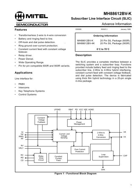
<strong>MH88612BV</strong>-K<br />
Subscriber Line Interface Circuit (SL<strong>IC</strong>)<br />
Advance Information<br />
Features<br />
• Transformerless 2-wire to 4-wire conversion<br />
• Battery and ringing feed to line.<br />
• Off-hook and dial pulse detection. .<br />
• Ring ground over-current protection.<br />
• Constant current feed with constant voltage<br />
foldover.<br />
• Relay driver.<br />
• Power Denial.<br />
• Wide Operating Range.<br />
• Pin for pin compatible 600R and 900R variants.<br />
Applications<br />
Line interface for:<br />
• PABX<br />
• Intercoms<br />
• Key Telephone Systems<br />
• Control Systems<br />
DS5066 ISSUE 2 January 1999<br />
<strong>MH88612BV</strong>-K<br />
<strong>MH88612BV</strong>-4K<br />
Description<br />
Ordering Information<br />
20 Pin SIL Package (600R)<br />
20 Pin SIL Package (900R)<br />
0°C to 70°C<br />
The SL<strong>IC</strong> provides a complete interface between a<br />
switching system and a subscriber loop. Functions<br />
provided include battery feed and ringing feed to the<br />
subscriber line, 2-Wire to 4-Wire hybrid interfacing,<br />
constant current feed with constant voltage foldback,<br />
and dial pulse detection. The device is fabricated<br />
using thick film hybrid technology in a 20-pin single<br />
in-line package.<br />
LPGND VBAT PD VCC VEE AGND<br />
Constant<br />
Voltage<br />
Foldback<br />
Power<br />
Management<br />
TF<br />
TIP<br />
RING<br />
RF<br />
Current and<br />
Voltage<br />
Sensing<br />
2-Wire to<br />
4-Wire<br />
Conversion<br />
VR<br />
VX<br />
RV<br />
VRLY<br />
RC<br />
RD<br />
CD<br />
Relay<br />
Drive<br />
Circuit<br />
Constant<br />
Current<br />
Feed<br />
Over Current<br />
Protection<br />
Loop<br />
Supervision<br />
CAP<br />
Figure 1 - Functional Block Diagram<br />
SHK<br />
1
<strong>MH88612BV</strong>-K<br />
Advance Information<br />
TF<br />
LPGND<br />
VR<br />
<strong>IC</strong><br />
VEE<br />
AGND<br />
PD<br />
VX<br />
TIP<br />
RING<br />
RF<br />
VCC<br />
RC<br />
RD<br />
RV<br />
VRLY<br />
CD<br />
VBAT<br />
CAP<br />
SHK<br />
1<br />
2<br />
3<br />
4<br />
5<br />
6<br />
7<br />
8<br />
9<br />
10<br />
11<br />
12<br />
13<br />
14<br />
15<br />
16<br />
17<br />
18<br />
19<br />
20<br />
Figure 2 - Pin Connections<br />
Pin Description<br />
Pin # Name Description<br />
1 TF Tip Feed. Connects to external diode for protection<br />
2 LPGND Loop Ground. Is the system ground reference with respect to VBAT. Normally connected<br />
to AGND.<br />
3 VR Voice Receive (Input). The 4 wire analog signal to the device.<br />
4 <strong>IC</strong> Internal Connection. No connection should be made to this pin<br />
5 VEE Negative Power Supply Voltage (-5V).<br />
6 AGND Analog Ground. Connects to System Ground (Earth).<br />
7 PD Power Denial (Input). A logic high will isolate the battery voltage to Tip/Ring.<br />
8 VX Voice Transmit (Output). The 4-wire analog signal from the device.<br />
9 TIP Tip Lead. Connects to the "Tip" lead of the telephone line.<br />
10 RING Ring Lead. Connects to the "Ring" lead of the telephone line.<br />
11 RF Ring Feed (Input). Normally connected to Ring relay for negative battery feed voltage and<br />
ringing voltage input.<br />
12 VCC Positive Power Supply Voltage (+5V).<br />
13 RC Relay Control (Input). Active high.<br />
14 RD Relay Drive. Open collector sinks current when RC is at logic high.<br />
15 RV Ring Feed Voltage. Normally connected to pin 11 (RF) through a normally closed relay<br />
and to external diode protection.<br />
16 VRLY Relay voltage Supply (+5V).<br />
17 CD Clamping Diode. Normally connected to AGND.<br />
18 VBAT Negative Battery Feed Supply Voltage (-48V). Battery supply for the Subscriber Line.<br />
Typically -48VDC is applied to this pin.<br />
19 CAP Ring Trip Filter Capacitor. Normally connected via an external capacitor to ground to<br />
prevent false ring trip. Must be open circuit to allow dial pulse detection.<br />
20 SHK Switch Hook Detect (Output). A logic level 1 will indicate that the Subscriber Line is in<br />
the ’Off-Hook’ state.<br />
Note 1: C4 in Figure 3 can be added permanently to this pin for certain dial pulse applications.<br />
2
Advance Information<br />
Functional Description<br />
The SL<strong>IC</strong> performs a transformerless 2-wire to 4-<br />
wire conversion of the analog signal. The 2-wire<br />
circuit is the balanced line going to the subscriber<br />
loop, while the 4-wire circuit is the audio signal going<br />
to and from devices such as the voice codec or<br />
switching circuit. The SL<strong>IC</strong> also provides a switch<br />
hook (SHK) status output which goes high when the<br />
telephone is set off-hook.<br />
Constant Current Feed<br />
The <strong>MH88612BV</strong>-K family employs complex<br />
feedback circuits to supply a constant current feed<br />
or, if necessary, constant voltage feed to the line.<br />
With a nominal -48V battery the device will supply a<br />
constant current of typically 25mA to a line up to<br />
1100Ω. For longer lines there is insufficient battery<br />
voltage so the device automatically switches to<br />
constant voltage mode where Tip and Ring will stay<br />
at their minimum and maximum voltage levels and<br />
the supplied current will be reduced accordingly. The<br />
maximum line resistance supported is 2000Ω<br />
including the telephone set.<br />
Switch Hook Detection<br />
The SHK pin will go to logic 1 to indicate that a<br />
telephone connected to the line has gone off-hook<br />
(on-line). Off-hook will not be indicated if the loop<br />
resistance (including the telephone set) is too high<br />
for the device to support.<br />
The SHK output will toggle to indicate dial pulses on<br />
the line. If the capacitor on CAP (Pin 19) has not<br />
been switched out of circuit the dial pulses will be<br />
distorted.<br />
Ringing And Ring Trip Detection<br />
In Figure 3 a ringing signal (e.g.90 Vrms and -48Vdc)<br />
is applied to the line by disconnecting pin 15 (RV)<br />
from pin 11(RF), and connecting the ringing voltage<br />
at pin 11 (RF) by use of the relay K1.<br />
The SL<strong>IC</strong> can detect an off-hook condition during<br />
ringing but there is a large AC component which<br />
must be filtered out to give a true off-hook condition<br />
at SHK.<br />
<strong>MH88612BV</strong>-K<br />
disconnect the ringing voltage from pin 11 and<br />
reconnect to pin 15. At that time the SL<strong>IC</strong> will revert<br />
to constant current feed operation.<br />
For applications requiring Dial Pulse Detection the<br />
Capacitor connection to ground C1 should be<br />
controlled such that the capacitor is disconnected<br />
during Pulse Dialling.<br />
If the signalling method is unknown, a capacitor of<br />
approximately 56nf should be permanently fitted<br />
between CAP (pin 19) and ground. This should be in<br />
addition to the capacitor mentioned in the above<br />
paragraph.<br />
During off-hook conditions (on-line), the capacitor<br />
(C1) should not have a low impedance path to<br />
ground. This can be achieved using a transistor (Q1)<br />
and resistor (R2) as shown in Figure 3, with R2<br />
providing a high impedance path for C1. When<br />
ringing is applied (RC = 5V) the transistor will short<br />
circuit R2 which will give C1 a low impedance path to<br />
ground and provide the required filtering.<br />
Other methods can be used to switch out C1, such<br />
as a relay or a codec system drive output (with a<br />
similar configuration as above).<br />
For applications using DTMF signalling, C1 can be<br />
permanently connected to ground.<br />
Current Limit<br />
The Tip or Ring of the telephone line may<br />
accidentally be shorted to ground. In such a case,<br />
current will only flow through the feed resistor. This<br />
high current will be sensed and reduced by the<br />
current limit circuit to a lower value to protect the<br />
internal circuitry.<br />
Power Denial<br />
The power denial function is a feature of the<br />
MH88612 which allows for powering down of the<br />
subscriber loop. A logic high voltage applied to the<br />
power denial input effectively removes the battery<br />
voltage from the loop driver circuitry. The resulting<br />
I LOOP is negligible and power consumption is<br />
minimised. The power denial function is useful for<br />
disabling a loop which may have a ground fault.<br />
A 1.0µF capacitor connected from pin 19 (CAP) to<br />
ground will provide adequate attenuation when<br />
ringing is applied. Once an off-hook condition has<br />
been detected a logic low should be applied to pin 13<br />
(RC) which will deactivate the relay (K1) to<br />
3
<strong>MH88612BV</strong>-K<br />
Advance Information<br />
~<br />
90<br />
-<br />
+<br />
R1<br />
VRMS<br />
48V<br />
K1<br />
D4<br />
D2<br />
VBAT<br />
D3<br />
D1<br />
11<br />
1<br />
15<br />
2<br />
RF<br />
TF<br />
RV<br />
LPGND<br />
<strong>MH88612BV</strong>-K<br />
VR<br />
VX<br />
3<br />
8<br />
TIP<br />
9<br />
TIP<br />
Protection<br />
Circuit<br />
SHK<br />
20<br />
RING<br />
+5V<br />
C2<br />
K1<br />
10<br />
13<br />
16<br />
14<br />
17<br />
RING<br />
RC<br />
VRLY<br />
RD<br />
CD<br />
VBAT<br />
VCC<br />
VEE<br />
PD<br />
CAP<br />
AGND<br />
7<br />
19 C1<br />
C4<br />
- +<br />
R2<br />
Q1<br />
R3 RC<br />
(Pin 13)<br />
R4<br />
18<br />
12<br />
5<br />
6<br />
C3<br />
-48V<br />
+5V<br />
-5V<br />
Component List<br />
= earth = ground<br />
R1 200Ω + 10%, 1/4W<br />
R2 470kΩ + 5%, 1/4W<br />
R3, R4 10kΩ + 5%, 1/4W<br />
C1<br />
1.0µF, + 10%, 25V electrolytic capacitor<br />
C2, C3 0.1µF, + 20%, 50V ceramic de-coupling capacitors<br />
D1,D2, D3, D4 Diode rectifier 200V, 1A, IN4003<br />
Q1<br />
General purpose switching transistor<br />
K1<br />
Relay E/M, 5V or 6V, 1 Form C<br />
C4<br />
10nF - 56nF 20% 16V capacitor<br />
Protection Circuit - Depending on the application the Protection circuit may need to provide<br />
over-voltage and/or over-current protection. In certain circumstances no protection will be required.<br />
Figure 3 - Typical Application Circuit<br />
.<br />
4
Advance Information<br />
<strong>MH88612BV</strong>-K<br />
Absolute Maximum Ratings*<br />
1 DC Supply Voltage<br />
LPGND = AGND<br />
Parameter Symbol Min Max Units<br />
V CC<br />
-0.3<br />
V EE<br />
-9<br />
V BAT<br />
-60<br />
V RLY -0.3<br />
2 Storage Temperature T S -40 100 °C<br />
3 Package Power Dissipation PD 2 W<br />
* Exceeding these values may cause permanent damage. Functional operation under these conditions is not implied.<br />
Recommended Operating Conditions<br />
4.75<br />
Characteristics Sym Min Typ‡ Max Units Test Conditions<br />
1 Operating Supply Voltage V CC<br />
5.0 5.25 V<br />
V RLY 5<br />
V<br />
V EE<br />
V BAT<br />
-5.25<br />
-54<br />
-5.0<br />
-48<br />
-4.75<br />
-42<br />
V<br />
V<br />
2 Relay Driver Current I RLY 100 mA<br />
3 T o 0 70 °C<br />
‡Typical figures are at 25˚C with nominal 5V supplies and are for design aid only.<br />
9<br />
0.3<br />
0.3<br />
40<br />
V<br />
V<br />
V<br />
V<br />
DC Electrical Characteristics † - Voltages are with respect to GNDA unless otherwise stated.<br />
Characteristics Sym Min Typ‡ Max Units Test Conditions<br />
1 Supply Current V CC<br />
V EE<br />
V BAT<br />
I CC<br />
7.5<br />
I EE<br />
-5.1<br />
I BAT<br />
2 Power Consumption P C 160<br />
1600<br />
3 Constant Current Line Feed I Loop 23<br />
15<br />
9 PD Control Input<br />
Input Low Current<br />
I IL<br />
0.5<br />
Input High Current<br />
I IH 0.3<br />
† DC Electrical Characteristics are over recommended operating supply voltages.<br />
‡Typical figures are at 25˚C with nominal 5V supplies and are for design aid only.<br />
3<br />
25<br />
16.5<br />
800<br />
27<br />
19<br />
mA<br />
mA<br />
µA<br />
mA<br />
mW<br />
mW<br />
mA<br />
mA<br />
PD = Logic High<br />
PD = Logic Low, Idle<br />
Standby V BAT = -48V<br />
Active (Off Hook)<br />
R Loop
<strong>MH88612BV</strong>-K<br />
Advance Information<br />
AC Electrical Characteristics<br />
Characteristics Sym Min Typ‡ Max Units Test Conditions<br />
1 Ringing Voltage<br />
Frequency<br />
‡Typical figure are at 25°C and are for design aid only.<br />
V RING<br />
F RING 17<br />
90<br />
25<br />
V rms<br />
Hz<br />
2 Ringer Equivalence Number REN 2<br />
3 Ring Trip Detect time 200 300 ms<br />
4 Input AC Impedance 2-wire Zin 600<br />
900<br />
5 Input Impedance at VR 100 kΩ<br />
6 Output Impedance at VX 10 Ω<br />
7 Gain 2-wire to VX<br />
-1.3 -1.0 -0.7 dB<br />
Gain relative to Gain @ 1kHz<br />
8 Gain VR to 2-wire<br />
Gain relative to Gain @ 1kHz<br />
9 2-wire Return Loss over<br />
300-3400Hz<br />
-0.3<br />
-1.3<br />
-0.3<br />
+0.3<br />
-1.0 -0.7<br />
+0.3<br />
Ω<br />
Ω<br />
dB<br />
dB<br />
Superimposed on V BAT =<br />
-48V<br />
<strong>MH88612BV</strong>-K<br />
<strong>MH88612BV</strong>-4K<br />
Input + 3dBm,<br />
1kHz across Tip and Ring<br />
300-3400 Hz<br />
Input 0.5Vrms 1kHz at VR<br />
Z Load = 600Ω<br />
300 - 3400 Hz<br />
20 30 dB Input 0.5Vrms,<br />
1kHz across Tip and Ring<br />
Z Load = 600Ω<br />
10 Transhybrid Loss THL 20 30 dB 300-3400 Hz<br />
Z Load = 600Ω<br />
11 Longitudinal to Metallic<br />
Balance<br />
12 Total Harmonic Distortion<br />
at VX<br />
at Tip and Ring<br />
13 Common Mode Rejection<br />
Ratio<br />
2-wire to VX<br />
THD<br />
CMRR<br />
40<br />
46<br />
55<br />
55<br />
0.1<br />
0.1<br />
40 50<br />
1.0<br />
1.0<br />
dB<br />
dB<br />
%<br />
%<br />
dB<br />
300-600Hz<br />
600-3400Hz<br />
Input + 3dBm,<br />
1kHz across Tip and Ring<br />
Input 1.0Vrms 1kHz at VR<br />
Input 0.5Vrms, 1kHz<br />
14 Idle channel Noise Nc +14 dBrnC @ 2 Wire and VX<br />
C- Message weighted<br />
15 Power supply rejection ratio<br />
V CC<br />
V EE<br />
V BAT<br />
PSRR<br />
26<br />
26<br />
26<br />
dB<br />
dB<br />
dB<br />
100 mV PP ripple, 1kHz on<br />
V CC /V EE /V BAT , measure at<br />
VX and across Tip and<br />
Ring<br />
6
Advance Information<br />
<strong>MH88612BV</strong>-K<br />
0.08 Max 0.12 Max<br />
(2.03 Max) (3.05 Max)<br />
2.02 Max<br />
(51.30 Max)<br />
0.50 max<br />
(12.70 max)<br />
1<br />
0.18 + 0.02<br />
(4.57 + 0.51)<br />
0.01 + 0.002<br />
(0.25 + 0.05)<br />
*<br />
0.05 + 0.02<br />
(1.27+ 0.51)<br />
* 0.10+ 0.01<br />
(2.54 + 0.25)<br />
0.02 + 0.005<br />
(0.51 + 0.13)<br />
Notes:<br />
1) Not to scale<br />
2) Dimensions in inches.<br />
(Dimensions in millimetres)<br />
3) Pin tolerances are non-accumulative.<br />
4) Recommended soldering conditions:<br />
wave soldering max. temp: 260˚C for<br />
10 secs.<br />
* Dimensions to centre of pin.<br />
Figure 4 - Mechanical Data<br />
7
http://www.mitelsemi.com<br />
World Headquarters - Canada<br />
Tel: +1 (613) 592 2122<br />
Fax: +1 (613) 592 6909<br />
North America Asia/Pacific Europe, Middle East,<br />
Tel: +1 (770) 486 0194 Tel: +65 333 6193 and Africa (EMEA)<br />
Fax: +1 (770) 631 8213 Fax: +65 333 6192 Tel: +44 (0) 1793 518528<br />
Fax: +44 (0) 1793 518581<br />
Information relating to products and services furnished herein by Mitel Corporation or its subsidiaries (collectively “Mitel”) is believed to be reliable. However, Mitel assumes no<br />
liability for errors that may appear in this publication, or for liability otherwise arising from the application or use of any such information, product or service or for any infringement of<br />
patents or other intellectual property rights owned by third parties which may result from such application or use. Neither the supply of such information or purchase of product or<br />
service conveys any license, either express or implied, under patents or other intellectual property rights owned by Mitel or licensed from third parties by Mitel, whatsoever.<br />
Purchasers of products are also hereby notified that the use of product in certain ways or in combination with Mitel, or non-Mitel furnished goods or services may infringe patents or<br />
other intellectual property rights owned by Mitel.<br />
This publication is issued to provide information only and (unless agreed by Mitel in writing) may not be used, applied or reproduced for any purpose nor form part of any order or<br />
contract nor to be regarded as a representation relating to the products or services concerned. The products, their specifications, services and other information appearing in this<br />
publication are subject to change by Mitel without notice. No warranty or guarantee express or implied is made regarding the capability, performance or suitability of any product or<br />
service. Information concerning possible methods of use is provided as a guide only and does not constitute any guarantee that such methods of use will be satisfactory in a specific<br />
piece of equipment. It is the user’s responsibility to fully determine the performance and suitability of any equipment using such information and to ensure that any publication or<br />
data used is up to date and has not been superseded. Manufacturing does not necessarily include testing of all functions or parameters. These products are not suitable for use in<br />
any medical products whose failure to perform may result in significant injury or death to the user. All products and materials are sold and services provided subject to Mitel’s<br />
conditions of sale which are available on request.<br />
M Mitel (design) and ST-BUS are registered trademarks of MITEL Corporation<br />
Mitel Semiconductor is an ISO 9001 Registered Company<br />
Copyright 1999 MITEL Corporation<br />
All Rights Reserved<br />
Printed in CANADA<br />
TECHN<strong>IC</strong>AL DOCUMENTATI<strong>ON</strong> - NOT FOR RESALE