Walsin Technology Corporation
Walsin Technology Corporation
Walsin Technology Corporation

You also want an ePaper? Increase the reach of your titles
YUMPU automatically turns print PDFs into web optimized ePapers that Google loves.
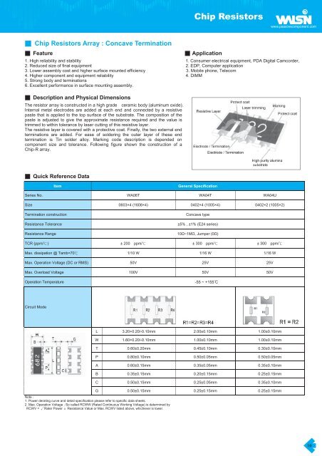
Chip Resistors<br />
www.passivecomponent.com<br />
Chip Resistors Array : Concave Termination<br />
Feature<br />
Application<br />
1. High reliability and stability 1. Consumer electrical equipment, PDA Digital Camcorder,<br />
2. Reduced size of final equipment 2. EDP, Computer application<br />
3. Lower assembly cost and higher surface mounted efficiency 3. Mobile phone, Telecom<br />
4. Higher component and equipment reliability 4. DIMM<br />
5. Strong body and terminations<br />
6. Excellent performance in surface mounting assembly.<br />
Description and Physical Dimensions<br />
The resistor array is constructed in a high grade ceramic body (aluminum oxide).<br />
Internal metal electrodes are added at each end and connected by a resistive<br />
paste that is applied to the top surface of the substrate. The composition of the<br />
paste is adjusted to give the approximate resistance required and the value is<br />
trimmed to within tolerance by laser cutting of this resistive layer.<br />
The resistive layer is covered with a protective coat. Finally, the two external end<br />
terminations are added. For ease of soldering the outer layer of these end<br />
termination is Tin solder alloy. Marking code description is depended on<br />
component size and tolerance. Following figure shown the construction of a<br />
Chip-R array.<br />
Quick Reference Data<br />
Item<br />
General Specification<br />
Series No. WA06T WA04T WA04U<br />
Size 0603×4 (1608×4) 0402×4 (1005×4) 0402×2 (1005×2)<br />
Termination construction<br />
Resistance Tolerance<br />
Resistance Range<br />
Concave type<br />
±5% , ±1% (E24 series)<br />
10~1M, Jumper (0)<br />
TCR (ppm/) ± 200 ppm/ ±300 ppm/ ±300 ppm/<br />
Max. dissipation @ Tamb=70 1/10 W 1/16 W 1/16 W<br />
Max. Operation Voltage (DC or RMS) 50V 25V 25V<br />
Max. Overload Voltage 100V 50V 50V<br />
Operation Temperature<br />
-55 ~ +155 C<br />
Circuit Mode<br />
L 3.20+0.20/-0.10mm 2.00±0.10mm 1.00±0.10mm<br />
W 1.60+0.20/-0.10mm 1.00±0.10mm 1.00±0.10mm<br />
T 0.60±0.20mm 0.45±0.10mm 0.30±0.10mm<br />
P 0.80±0.10mm 0.50±0.05mm 0.50±0.05mm<br />
A 0.60±0.15mm 0.35±0.05mm 0.35±0.10mm<br />
B 0.35±0.15mm 0.20±0.15mm 0.25±0.15mm<br />
C 0.50±0.15mm 0.25±0.05mm 0.35±0.10mm<br />
G 0.50±0.15mm 0.25±0.15mm 0.25±0.15mm<br />
Note :<br />
1. Power derating curve and detail specification please refer to specific data sheets.<br />
2. Max. Operation Voltage : So called RCWW (Rated Continuous Working Voltage) is determined by<br />
RCWV = Rater Power × Resistance Value or Max. RCWV listed above, whichever is lower.<br />
10