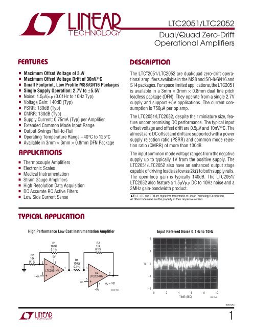
LTC2051/LTC2052 Dual/Quad Zero-Drift Operational Amplifiers ...
LTC2051/LTC2052 Dual/Quad Zero-Drift Operational Amplifiers ...
LTC2051/LTC2052 Dual/Quad Zero-Drift Operational Amplifiers ...

Create successful ePaper yourself
Turn your PDF publications into a flip-book with our unique Google optimized e-Paper software.
<strong>LTC2051</strong>/<strong>LTC2052</strong><br />
<strong>Dual</strong>/<strong>Quad</strong> <strong>Zero</strong>-<strong>Drift</strong><br />
<strong>Operational</strong> <strong>Amplifiers</strong><br />
FEATURES<br />
■ Maximum Offset Voltage of 3μV<br />
■ Maximum Offset Voltage <strong>Drift</strong> of 30nV/°C<br />
■ Small Footprint, Low Profile MS8/GN16 Packages<br />
■ Single Supply Operation: 2.7V to ±5.5V<br />
■ Noise: 1.5μV P-P (0.01Hz to 10Hz Typ)<br />
■ Voltage Gain: 140dB (Typ)<br />
■ PSRR: 130dB (Typ)<br />
■ CMRR: 130dB (Typ)<br />
■ Supply Current: 0.75mA (Typ) per Amplifier<br />
■ Extended Common Mode Input Range<br />
■ Output Swings Rail-to-Rail<br />
■ Operating Temperature Range –40°C to 125°C<br />
■ Available in 3mm × 3mm × 0.8mm DFN Package<br />
APPLICATIO S<br />
U<br />
■<br />
■<br />
■<br />
■<br />
■<br />
■<br />
■<br />
Thermocouple <strong>Amplifiers</strong><br />
Electronic Scales<br />
Medical Instrumentation<br />
Strain Gauge <strong>Amplifiers</strong><br />
High Resolution Data Acquisition<br />
DC Accurate RC Active Filters<br />
Low Side Current Sense<br />
DESCRIPTIO<br />
U<br />
The LTC ® 2051/<strong>LTC2052</strong> are dual/quad zero-drift operational<br />
amplifiers available in the MS8 and SO-8/GN16 and<br />
S14 packages. For space limited applications, the <strong>LTC2051</strong><br />
is available in a 3mm × 3mm × 0.8mm dual fine pitch<br />
leadless package (DFN). They operate from a single 2.7V<br />
supply and support ±5V applications. The current consumption<br />
is 750μA per op amp.<br />
The <strong>LTC2051</strong>/<strong>LTC2052</strong>, despite their miniature size, feature<br />
uncompromising DC performance. The typical input<br />
offset voltage and offset drift are 0.5μV and 10nV/°C. The<br />
almost zero DC offset and drift are supported with a power<br />
supply rejection ratio (PSRR) and common mode rejection<br />
ratio (CMRR) of more than 130dB.<br />
The input common mode voltage ranges from the negative<br />
supply up to typically 1V from the positive supply. The<br />
<strong>LTC2051</strong>/<strong>LTC2052</strong> also have an enhanced output stage<br />
capable of driving loads as low as 2kΩ to both supply rails.<br />
The open-loop gain is typically 140dB. The <strong>LTC2051</strong>/<br />
<strong>LTC2052</strong> also feature a 1.5μV P-P DC to 10Hz noise and a<br />
3MHz gain-bandwidth product.<br />
, LT, LTC and LTM are registered trademarks of Linear Technology Corporation.<br />
All other trademarks are the property of their respective owners.<br />
TYPICAL APPLICATIO<br />
U<br />
High Performance Low Cost Instrumentation Amplifier<br />
R2<br />
10k<br />
0.1%<br />
2<br />
R1<br />
100Ω<br />
0.1%<br />
5V<br />
8<br />
R1<br />
100Ω<br />
0.1%<br />
R2<br />
10k<br />
0.1%<br />
–<br />
1/2 1<br />
6<br />
<strong>LTC2051</strong>HV<br />
–<br />
3<br />
1/2 7<br />
–V IN +<br />
<strong>LTC2051</strong>HV<br />
5<br />
V IN +<br />
A V = 101<br />
–5V<br />
4<br />
20512 TA01<br />
μV<br />
2<br />
1<br />
0<br />
–1<br />
–2<br />
Input Referred Noise 0.1Hz to 10Hz<br />
0 2 4 6 8 10<br />
TIME (SEC)<br />
2052 TA02<br />
20512fc<br />
1
<strong>LTC2051</strong>/<strong>LTC2052</strong><br />
ABSOLUTE AXI U RATI GS<br />
W W W<br />
(Note 1)<br />
Total Supply Voltage (V + to V – )<br />
<strong>LTC2051</strong>/<strong>LTC2052</strong> .................................................. 7V<br />
<strong>LTC2051</strong>HV/<strong>LTC2052</strong>HV ....................................... 12V<br />
Input Voltage (Note 5) .......... (V + + 0.3V) to (V – – 0.3V)<br />
Output Short-Circuit Duration ......................... Indefinite<br />
U<br />
Operating Temperature Range ............. – 40°C to 125°C<br />
Specified Temperature Range (Note 3) – 40°C to 125°C<br />
Storage Temperature Range ................ – 65°C to 150°C<br />
DD Package ...................................... –65°C to 125°C<br />
Lead Temperature (Soldering, 10 sec)................. 300°C<br />
U U W<br />
PACKAGE/ORDER I FOR ATIO<br />
TOP VIEW<br />
OUT A 1<br />
8 V +<br />
–IN A<br />
+IN A<br />
V – 2<br />
3<br />
4<br />
7<br />
6<br />
5<br />
OUT B<br />
–IN B<br />
+IN B<br />
DD PACKAGE<br />
8-LEAD (3mm × 3mm) PLASTIC DFN<br />
T JMAX = 125°C, θ JA = 160°C/W<br />
OUT A<br />
–IN A<br />
+IN A<br />
TOP VIEW<br />
V – 1<br />
2<br />
3<br />
4<br />
8<br />
7<br />
6<br />
5<br />
MS8 PACKAGE<br />
8-LEAD PLASTIC MSOP<br />
V +<br />
OUT B<br />
–IN B<br />
+IN B<br />
T JMAX = 125°C, θ JA = 250°C/W<br />
OUT A<br />
–IN A<br />
+IN A<br />
V –<br />
SHDN A<br />
1<br />
2<br />
3<br />
4<br />
5<br />
TOP VIEW<br />
10<br />
9<br />
8<br />
7<br />
6<br />
MS10 PACKAGE<br />
10-LEAD PLASTIC MSOP<br />
T JMAX = 125°C, θ JA = 250°C/W<br />
V +<br />
OUT B<br />
–IN B<br />
+IN B<br />
SHDN B<br />
ORDER PART<br />
NUMBER*<br />
<strong>LTC2051</strong>CDD<br />
<strong>LTC2051</strong>IDD<br />
<strong>LTC2051</strong>HVCDD<br />
<strong>LTC2051</strong>HVIDD<br />
OUT A 1<br />
–IN A 2<br />
+IN A 3<br />
V – 4<br />
DD PART<br />
MARKING<br />
LAAN<br />
LAEL<br />
TOP VIEW<br />
8<br />
7<br />
6<br />
5<br />
S8 PACKAGE<br />
8-LEAD PLASTIC SO<br />
T JMAX = 125°C, θ JA = 190°C/W<br />
V +<br />
OUT B<br />
–IN B<br />
+IN B<br />
Order Options Tape and Reel: Add #TR<br />
Lead Free: Add #PBF Lead Free Tape and Reel: Add #TRPBF<br />
Lead Free Part Marking: http://www.linear.com/leadfree/<br />
ORDER PART<br />
NUMBER<br />
<strong>LTC2051</strong>CMS8<br />
<strong>LTC2051</strong>IMS8<br />
<strong>LTC2051</strong>HVCMS8<br />
<strong>LTC2051</strong>HVIMS8<br />
<strong>LTC2051</strong>HMS8<br />
<strong>LTC2051</strong>HVHMS8<br />
Consult LTC Marketing for parts specified with wider operating temperature ranges.<br />
MS8 PART<br />
MARKING<br />
LTMN<br />
LTMP<br />
LTPJ<br />
LTPK<br />
LTVF<br />
LTVH<br />
ORDER PART<br />
NUMBER<br />
<strong>LTC2051</strong>CS8<br />
<strong>LTC2051</strong>IS8<br />
<strong>LTC2051</strong>HVCS8<br />
<strong>LTC2051</strong>HVIS8<br />
<strong>LTC2051</strong>HS8<br />
<strong>LTC2051</strong>HVHS8<br />
ORDER PART<br />
NUMBER<br />
<strong>LTC2051</strong>CMS10<br />
<strong>LTC2051</strong>IMS10<br />
<strong>LTC2051</strong>HVCMS10<br />
<strong>LTC2051</strong>HVIMS10<br />
MS10 PART<br />
MARKING<br />
LTMQ<br />
LTMR<br />
LTRB<br />
LTRC<br />
S8 PART<br />
MARKING<br />
2051<br />
2051I<br />
2051HV<br />
051HVI<br />
2051H<br />
051HVH<br />
2<br />
20512fc
<strong>LTC2051</strong>/<strong>LTC2052</strong><br />
U W<br />
PACKAGE/ORDER I FOR ATIO<br />
U<br />
OUT A<br />
–IN A<br />
+IN A<br />
V +<br />
+IN B<br />
–IN B<br />
OUT B<br />
NC<br />
1<br />
2<br />
3<br />
4<br />
5<br />
6<br />
7<br />
8<br />
TOP VIEW<br />
GN PACKAGE<br />
16-LEAD PLASTIC SSOP<br />
16 OUT D<br />
15 –IN D<br />
14 +IN D<br />
13 V –<br />
12 +IN C<br />
11 –IN C<br />
10 OUT C<br />
9 NC<br />
T JMAX = 125°C, θ JA = 110°C/W<br />
ORDER PART<br />
NUMBER<br />
<strong>LTC2052</strong>CGN<br />
<strong>LTC2052</strong>IGN<br />
<strong>LTC2052</strong>HVCGN<br />
<strong>LTC2052</strong>HVIGN<br />
<strong>LTC2052</strong>HGN<br />
<strong>LTC2052</strong>HVHGN<br />
GN PART MARKING<br />
2052<br />
2052I<br />
2052HV<br />
052HVI<br />
2052H<br />
052HVH<br />
OUT A 1<br />
–IN A 2<br />
+IN A 3<br />
V + 4<br />
+IN B 5<br />
–IN B 6<br />
OUT B 7<br />
TOP VIEW<br />
S PACKAGE<br />
14-LEAD PLASTIC SO<br />
14 OUT D<br />
13 –IN D<br />
12 +IN D<br />
11 V –<br />
10 +IN C<br />
9 –IN C<br />
8 OUT C<br />
T JMAX = 125°C, θ JA = 110°C/W<br />
ORDER PART<br />
NUMBER<br />
<strong>LTC2052</strong>CS<br />
<strong>LTC2052</strong>IS<br />
<strong>LTC2052</strong>HVCS<br />
<strong>LTC2052</strong>HVIS<br />
<strong>LTC2052</strong>HS<br />
<strong>LTC2052</strong>HVHS<br />
AVAILABLE OPTIO S<br />
U<br />
PART NUMBER AMPS/PACKAGE SPECIFIED TEMP RANGE SPECIFIED VOLTAGE PACKAGE<br />
<strong>LTC2051</strong>CDD 2 0°C to 70°C 3V, 5V DD<br />
<strong>LTC2051</strong>CS8 2 0°C to 70°C 3V, 5V SO-8<br />
<strong>LTC2051</strong>CMS8 2 0°C to 70°C 3V, 5V 8-Lead MSOP<br />
<strong>LTC2051</strong>CMS10 2 0°C to 70°C 3V, 5V 10-Lead MSOP<br />
<strong>LTC2051</strong>HVCDD 2 0°C to 70°C 3V, 5V, ±5V DD<br />
<strong>LTC2051</strong>HVCS8 2 0°C to 70°C 3V, 5V, ±5V SO-8<br />
<strong>LTC2051</strong>HVCMS8 2 0°C to 70°C 3V, 5V, ±5V 8-Lead MSOP<br />
<strong>LTC2051</strong>HVCMS10 2 0°C to 70°C 3V, 5V, ±5V 10-Lead MSOP<br />
<strong>LTC2051</strong>IDD 2 –40°C to 85°C 3V, 5V DD<br />
<strong>LTC2051</strong>IS8 2 –40°C to 85°C 3V, 5V SO-8<br />
<strong>LTC2051</strong>IMS8 2 –40°C to 85°C 3V, 5V 8-Lead MSOP<br />
<strong>LTC2051</strong>IMS10 2 –40°C to 85°C 3V, 5V 10-Lead MSOP<br />
<strong>LTC2051</strong>HVIDD 2 –40°C to 85°C 3V, 5V, ±5V DD<br />
<strong>LTC2051</strong>HVIS8 2 –40°C to 85°C 3V, 5V, ±5V SO-8<br />
<strong>LTC2051</strong>HVIMS8 2 –40°C to 85°C 3V, 5V, ±5V 8-Lead MSOP<br />
<strong>LTC2051</strong>HVIMS10 2 –40°C to 85°C 3V, 5V, ±5V 10-Lead MSOP<br />
<strong>LTC2051</strong>HS8 2 –40°C to 125°C 3V, 5V SO-8<br />
<strong>LTC2051</strong>HMS8 2 –40°C to 125°C 3V, 5V 8-Lead MSOP<br />
<strong>LTC2051</strong>HVHS8 2 –40°C to 125°C 3V, 5V, ±5V SO-8<br />
<strong>LTC2051</strong>HVHMS8 2 –40°C to 125°C 3V, 5V, ±5V 8-Lead MSOP<br />
<strong>LTC2052</strong>CS 4 0°C to 70°C 3V, 5V 14-Lead SO<br />
<strong>LTC2052</strong>CGN 4 0°C to 70°C 3V, 5V 16-Lead SSOP<br />
<strong>LTC2052</strong>HVCS 4 0°C to 70°C 3V, 5V, ±5V 14-Lead SO<br />
<strong>LTC2052</strong>HVCGN 4 0°C to 70°C 3V, 5V, ±5V 16-Lead SSOP<br />
20512fc<br />
3
<strong>LTC2051</strong>/<strong>LTC2052</strong><br />
AVAILABLE OPTIO S<br />
U<br />
PART NUMBER AMPS/PACKAGE SPECIFIED TEMP RANGE SPECIFIED VOLTAGE PACKAGE<br />
<strong>LTC2052</strong>IS 4 –40°C to 85°C 3V, 5V 14-Lead SO<br />
<strong>LTC2052</strong>IGN 4 –40°C to 85°C 3V, 5V 16-Lead SSOP<br />
<strong>LTC2052</strong>HVIS 4 –40°C to 85°C 3V, 5V, ±5V 14-Lead SO<br />
<strong>LTC2052</strong>HVIGN 4 –40°C to 85°C 3V, 5V, ±5V 16-Lead SSOP<br />
<strong>LTC2052</strong>HS 4 –40°C to 125°C 3V, 5V 14-Lead SO<br />
<strong>LTC2052</strong>HGN 4 –40°C to 125°C 3V, 5V 16-Lead SSOP<br />
<strong>LTC2052</strong>HVHS 4 –40°C to 125°C 3V, 5V, ±5V 14-Lead SO<br />
<strong>LTC2052</strong>HVHGN 4 –40°C to 125°C 3V, 5V, ±5V 16-Lead SSOP<br />
ELECTRICAL CHARACTERISTICS<br />
(<strong>LTC2051</strong>/<strong>LTC2052</strong>, <strong>LTC2051</strong>HV/<strong>LTC2052</strong>HV) The ● denotes the<br />
specifications which apply over the full operating temperature range, otherwise specifications are at T A = 25°C. V S = 3V, 5V<br />
unless otherwise noted. (Note 3)<br />
<strong>LTC2051</strong>C/<strong>LTC2052</strong>C<br />
<strong>LTC2051</strong>I/<strong>LTC2052</strong>I <strong>LTC2051</strong>H/<strong>LTC2052</strong>H<br />
PARAMETER CONDITIONS MIN TYP MAX MIN TYP MAX UNITS<br />
Input Offset Voltage (Note 2) ±0.5 ±3 ±0.5 ±3 μV<br />
Average Input Offset <strong>Drift</strong> (Note 2) ● 0.01 ±0.03 0.01 ±0.05 μV/°C<br />
Long-Term Offset <strong>Drift</strong> 50 50 nV/√mo<br />
Input Bias Current (Note 4) V S = 3V ±8 ±50 ±8 ±50 pA<br />
V S = 3V ● ±100 ±3000 pA<br />
V S = 5V ±25 ±75 ±25 ±75 pA<br />
V S = 5V ● ±150 ±3000 pA<br />
Input Offset Current (Note 4) V S = 3V ±100 ±100 pA<br />
V S = 3V ● ±150 ±700 pA<br />
V S = 5V ±150 ±150 pA<br />
V S = 5V ● ±200 ±700 pA<br />
Input Noise Voltage R S = 100Ω, DC to 10Hz 1.5 1.5 μV P-P<br />
Common Mode Rejection Ratio V CM = GND to V + – 1.3, 115 130 115 130 dB<br />
V S = 3V ● 110 130 110 130 dB<br />
V CM = GND to V + – 1.3, 120 130 120 130 dB<br />
V S = 5V ● 115 130 115 130 dB<br />
Power Supply Rejection Ratio 120 130 120 130 dB<br />
● 115 130 115 130 dB<br />
Large-Signal Voltage Gain R L = 10k, V S = 3V 120 140 120 140 dB<br />
● 115 140 115 140 dB<br />
R L = 10k, V S = 5V 125 140 125 140 dB<br />
● 120 140 120 140 dB<br />
Output Voltage Swing High R L = 2k to GND ● V + – 0.15 V + – 0.06 V + – 0.15 V + – 0.06 V<br />
R L = 10k to GND ● V + – 0.05 V + – 0.02 V + – 0.05 V + – 0.02 V<br />
Output Voltage Swing Low R L = 2k to GND ● 2 15 2 15 mV<br />
R L = 10k to GND ● 2 15 2 15 mV<br />
Slew Rate 2 2 V/μs<br />
Gain Bandwidth Product 3 3 MHz<br />
Supply Current (Per Amplifier) No Load, V S = 3V, V SHDN = V IH ● 0.75 1.0 0.75 1.1 mA<br />
No Load, V S = 5V, V SHDN = V IH ● 0.85 1.2 0.85 1.3 mA<br />
Supply Current, Shutdown V SHDN = V IL , V S = 3V ● 2 5 2 5 μA<br />
V SHDN = V IL , V S = 5V ● 4 10 4 10 μA<br />
4<br />
20512fc
ELECTRICAL CHARACTERISTICS<br />
<strong>LTC2051</strong>/<strong>LTC2052</strong><br />
(<strong>LTC2051</strong>/<strong>LTC2052</strong>, <strong>LTC2051</strong>HV/<strong>LTC2052</strong>HV) The ● denotes the<br />
specifications which apply over the full operating temperature range, otherwise specifications are at T A = 25°C. V S = 3V, 5V<br />
unless otherwise noted. (Note 3)<br />
<strong>LTC2051</strong>C/<strong>LTC2052</strong>C<br />
<strong>LTC2051</strong>I/<strong>LTC2052</strong>I <strong>LTC2051</strong>H/<strong>LTC2052</strong>H<br />
PARAMETER CONDITIONS MIN TYP MAX MIN TYP MAX UNITS<br />
Shutdown Pin Input Low Voltage (V IL ) ● V – + 0.5 V – + 0.5 V<br />
Shutdown Pin Input High Voltage (V IH ) ● V + – 0.5 V + – 0.5 V<br />
Shutdown Pin Input Current V SHDN = V IL , V S = 3V ● –1 –3 –1 –3 μA<br />
V SHDN = V IL , V S = 5V ● –2 –5 –2 –5 μA<br />
Internal Sampling Frequency 7.5 7.5 kHz<br />
(<strong>LTC2051</strong>HV/<strong>LTC2052</strong>HV) The ● denotes the specifications which apply over the full operating temperature range, otherwise<br />
specifications are at T A = 25°C. V S = ±5V unless otherwise noted. (Note 3)<br />
<strong>LTC2051</strong>C/<strong>LTC2052</strong>C<br />
<strong>LTC2051</strong>I/<strong>LTC2052</strong>I <strong>LTC2051</strong>H/<strong>LTC2052</strong>H<br />
PARAMETER CONDITIONS MIN TYP MAX MIN TYP MAX UNITS<br />
Input Offset Voltage (Note 2) ±1 ±3 ±1 ±3 μV<br />
Average Input Offset <strong>Drift</strong> (Note 2) ● 0.01 ±0.03 0.01 ±0.05 μV/°C<br />
Long-Term Offset <strong>Drift</strong> 50 50 nV/√mo<br />
Input Bias Current (Note 4) ±90 ±150 ±90 ±150 pA<br />
● ±300 ±3000 pA<br />
Input Offset Current (Note 4) ±300 ±300 pA<br />
● ±500 ±700 pA<br />
Input Noise Voltage R S = 100Ω, DC to 10Hz 1.5 1.5 μV P-P<br />
Common Mode Rejection Ratio V CM = V – to V + – 1.3 125 130 125 130 dB<br />
● 120 130 120 130 dB<br />
Power Supply Rejection Ratio 120 130 120 130 dB<br />
● 115 130 115 130 dB<br />
Large-Signal Voltage Gain R L = 10k 125 140 125 140 dB<br />
● 120 140 120 140 dB<br />
Maximum Output Voltage Swing R L = 2k to GND ● ±4.75 ±4.92 ±4.50 ±4.92 V<br />
R L = 10k to GND ● ±4.90 ±4.98 ±4.85 ±4.98 V<br />
Slew Rate 2 2 V/μs<br />
Gain Bandwidth Product 3 3 MHz<br />
Supply Current (Per Amplifier) No Load, V SHDN = V IH ● 1 1.5 1 1.5 mA<br />
Supply Current, Shutdown V SHDN = V IL ● 15 30 15 30 μA<br />
Shutdown Pin Input Low Voltage (V IL ) ● V – + 0.5 V – + 0.5 V<br />
Shutdown Pin Input High Voltage (V IH ) ● V + – 0.5 V + – 0.5 V<br />
Shutdown Pin Input Current V SHDN = V IL ● –7 –15 –7 –15 μA<br />
Internal Sampling Frequency 7.5 7.5 kHz<br />
Note 1: Stresses beyond those listed under Absolute Maximum Ratings<br />
may cause permanent damage to the device. Exposure to any Absolute<br />
Maximum Rating condition for extended periods may affect device<br />
reliability and lifetime.<br />
Note 2: These parameters are guaranteed by design. Thermocouple effects<br />
preclude measurements of these voltage levels during automated testing.<br />
Note 3: All versions of the <strong>LTC2051</strong>/<strong>LTC2052</strong> are designed, characterized<br />
and expected to meet the extended temperature limits of –40°C and 125°C.<br />
The <strong>LTC2051</strong>C/<strong>LTC2052</strong>C/<strong>LTC2051</strong>HVC/<strong>LTC2052</strong>HVC are guaranteed to<br />
meet the temperature limits of 0°C and 70°C. The <strong>LTC2051</strong>I/<strong>LTC2052</strong>I/<br />
<strong>LTC2051</strong>HVI/<strong>LTC2052</strong>HVI are guaranteed to meet temperature limits of –<br />
40°C and 85°C. The <strong>LTC2051</strong>H/<strong>LTC2051</strong>HVH and <strong>LTC2052</strong>H/<strong>LTC2052</strong>HVH<br />
are guaranteed to meet the temperature limits of –40°C and 125°C.<br />
Note 4: The bias current measurement accuracy depends on the proximity of<br />
the negative supply bypass capacitors to the device under test. Because of<br />
this, only the bias current of channel B (<strong>LTC2051</strong>) and channels A and B<br />
(<strong>LTC2052</strong>) are 100% tested to the data sheet specifications. The bias<br />
currents of the remaining channels are 100% tested to relaxed limits,<br />
however, their values are guaranteed by design to meet the data sheet limits.<br />
Note 5: This parameter is guaranteed to meet specified performance<br />
through design and characterization. It has not been tested.<br />
Note 6: The θ JA specified for the DD package is with minimal PCB heat<br />
spreading metal. Using expanded metal area on all layers of a board<br />
reduces this value.<br />
20512fc<br />
5
<strong>LTC2051</strong>/<strong>LTC2052</strong><br />
TYPICAL PERFOR A CE CHARACTERISTICS<br />
UW<br />
CMRR (dB)<br />
140<br />
120<br />
100<br />
80<br />
60<br />
40<br />
Common Mode Rejection Ratio<br />
vs Frequency<br />
V S = 3V OR ±5V<br />
V CM = 0.5V P-P<br />
CMRR (dB)<br />
140<br />
120<br />
100<br />
80<br />
60<br />
40<br />
DC CMRR<br />
vs Common Mode Input Range<br />
V S = 3V<br />
V S = 5V<br />
V S = 10V<br />
PSRR (dB)<br />
120<br />
100<br />
80<br />
60<br />
40<br />
PSRR vs Frequency<br />
+PSRR<br />
–PSRR<br />
20<br />
20<br />
20<br />
0<br />
1 10 100 1k 10k 100k<br />
FREQUENCY (Hz)<br />
20512 G01<br />
0<br />
0<br />
2 4 6 8 10<br />
V CM (V)<br />
20512 G02<br />
0<br />
10 100 1k 10k 100k 1M<br />
FREQUENCY (Hz)<br />
20512 G03<br />
6<br />
5<br />
Output Voltage Swing<br />
vs Load Resistance<br />
R L TO GND<br />
V S = 5V<br />
6<br />
5<br />
Output Swing vs Output Current<br />
V S = 5V<br />
5<br />
4<br />
3<br />
Output Swing<br />
vs Load Resistance ±5V<br />
R L TO GND<br />
OUTPUT SWING (V)<br />
4<br />
3<br />
2<br />
V S = 3V<br />
OUTPUT VOLTAGE (V)<br />
4<br />
3<br />
2<br />
V S = 3V<br />
OUTPUT VOLTAGE (V)<br />
2<br />
1<br />
0<br />
–1<br />
–2<br />
1<br />
1<br />
–3<br />
–4<br />
0<br />
0<br />
2 4 6 8<br />
LOAD RESISTANCE (kΩ)<br />
10<br />
0<br />
0.01<br />
0.1 1 10<br />
OUTPUT CURRENT (mA)<br />
–5<br />
0<br />
2 4 6 8 10<br />
LOAD RESISTANCE (kΩ)<br />
20512 G04<br />
20512 G05<br />
20512 G06<br />
OUTPUT SWING (V)<br />
5<br />
4<br />
3<br />
2<br />
1<br />
0<br />
–1<br />
–2<br />
–3<br />
–4<br />
–5<br />
0.01<br />
Output Swing<br />
vs Output Current, ±5V Supply<br />
R L TO GND<br />
0.1 1<br />
OUTPUT CURRENT (mA)<br />
20512 G07<br />
10<br />
GAIN (dB)<br />
100<br />
80<br />
Gain/Phase vs Frequency<br />
PHASE<br />
60<br />
GAIN<br />
120<br />
40<br />
140<br />
20<br />
160<br />
0<br />
–20<br />
V S = 3V OR ±5V<br />
C L = 50pF<br />
180<br />
R L = 100k<br />
–40<br />
200<br />
100 1k 10k 100k 1M 10M<br />
FREQUENCY (Hz)<br />
20512 G08<br />
80<br />
100<br />
PHASE (DEG)<br />
BIAS CURRENT (pA)<br />
10k<br />
1k<br />
100<br />
10<br />
Bias Current vs Temperature<br />
V S = ±5V<br />
V S = 5V<br />
V S = 3V<br />
1<br />
–50 0 50 100 125<br />
TEMPERATURE (°C)<br />
20512 G09<br />
6<br />
20512fc
<strong>LTC2051</strong>/<strong>LTC2052</strong><br />
TYPICAL PERFOR A CE CHARACTERISTICS<br />
UW<br />
Input Bias Current<br />
vs Input Common Mode Voltage<br />
Transient Response<br />
Input Overload Recovery<br />
250<br />
INPUT BIAS CURRENT (pA)<br />
200<br />
150<br />
100<br />
50<br />
0<br />
–5<br />
V S = ±5V<br />
V S = 5V<br />
V S = 3V<br />
–3 –1 0 1 3 5<br />
INPUT COMMON MODE VOLTAGE (V)<br />
2V/DIV<br />
A V = 1<br />
R L = 10k<br />
C L = 100pF<br />
V S = ±5V<br />
1μs/DIV<br />
20512 G11<br />
INPUT (V)<br />
OUTPUT (V)<br />
0<br />
–0.1<br />
1.5<br />
0<br />
A V = – 100<br />
R L = 100k<br />
C L = 10pF<br />
V S = 3V<br />
500μs/DIV<br />
2050 G12<br />
20512 G10<br />
10<br />
Sampling Frequency<br />
vs Supply Voltage<br />
10<br />
Sampling Frequency<br />
vs Temperature<br />
SAMPLING FREQUENCY (kHz)<br />
9<br />
8<br />
7<br />
6<br />
SAMPLING FREQUENCY (kHz)<br />
9<br />
8<br />
7<br />
6<br />
V S = ±5V<br />
V S = 3V<br />
5<br />
3<br />
5 7 9<br />
SUPPLY VOLTAGE (V)<br />
11<br />
5<br />
–50<br />
0 50 100<br />
TEMPERATURE (°C)<br />
125<br />
20512 G13<br />
20512 G14<br />
1.2<br />
1.0<br />
Supply Current (Per Amplifier)<br />
vs Supply Voltage<br />
1.2<br />
1.0<br />
Supply Current (Per Amplifier)<br />
vs Temperature<br />
V S = ±5V<br />
SUPPLY CURRENT (mA)<br />
0.8<br />
0.6<br />
0.4<br />
SUPPLY CURRENT (mA)<br />
0.8<br />
0.6<br />
0.4<br />
V S = 5V<br />
V S = 3V<br />
0.2<br />
0.2<br />
0<br />
2.5<br />
4.5 6.5 8.5 10.5<br />
SUPPLY VOLTAGE (V)<br />
0<br />
–50<br />
0 50 100<br />
TEMPERATURE (°C)<br />
125<br />
20512 G15<br />
20512 G16<br />
20512fc<br />
7
<strong>LTC2051</strong>/<strong>LTC2052</strong><br />
APPLICATIO S I FOR ATIO<br />
Shutdown<br />
U W U U<br />
The <strong>LTC2051</strong> includes a shutdown pin in the 10-lead<br />
MSOP. When this active low pin is high or allowed to float,<br />
the device operates normally. When the shutdown pin is<br />
pulled low, the device enters shutdown mode; supply<br />
current drops to 3μA, all clocking stops and the output<br />
assumes a high impedance state.<br />
Clock Feedthrough, Input Bias Current<br />
The <strong>LTC2051</strong>/<strong>LTC2052</strong> use autozeroing circuitry to achieve<br />
an almost zero DC offset over temperature, common<br />
mode voltage and power supply voltage. The frequency of<br />
the clock used for autozeroing is typically 7.5kHz. The<br />
term clock feedthrough is broadly used to indicate visibility<br />
of this clock frequency in the op amp output spectrum.<br />
There are typically two types of clock feedthrough in<br />
autozeroed op amps like the <strong>LTC2051</strong>/<strong>LTC2052</strong>.<br />
The first form of clock feedthough is caused by the settling<br />
of the internal sampling capacitor and is input referred;<br />
that is, it is multiplied by the closed-loop gain of the op<br />
amp. This form of clock feedthrough is independent of the<br />
magnitude of the input source resistance or the magnitude<br />
of the gain setting resistors. The <strong>LTC2051</strong>/<strong>LTC2052</strong> have<br />
a residue clock feedthrough of less than 1μV RMS input<br />
referred at 7.5kHz.<br />
The second form of clock feedthrough is caused by the<br />
small amount of charge injection occurring during the<br />
sampling and holding of the op amps input offset voltage.<br />
The current spikes are multiplied by the impedance seen<br />
at the input terminals of the op amp, appearing at the<br />
output multiplied by the closed-loop gain of the op amp.<br />
To reduce this form of clock feedthrough, use smaller<br />
valued gain setting resistors and minimize the source<br />
resistance at the input. If the resistance seen at the inputs<br />
is less than 10k, this form of clock feedthrough is less<br />
than 1μV RMS input referred at 7.5kHz, or less than the<br />
amount of residue clock feedthrough from the first form<br />
previously described.<br />
Placing a capacitor across the feedback resistor reduces<br />
either form of clock feedthrough by limiting the bandwidth<br />
of the closed-loop gain.<br />
Input bias current is defined as the DC current into the<br />
input pins of the op amp. The same current spikes that<br />
cause the second form of clock feedthrough previously<br />
described, when averaged, dominate the DC input bias<br />
current of the op amp below 70°C.<br />
At temperatures above 70°C, the leakage of the ESD<br />
protection diodes on the inputs increase the input bias<br />
currents of both inputs in the positive direction, while the<br />
current caused by the charge injection stays relatively<br />
constant. At elevated temperatures (above 85°C) the<br />
leakage current begins to dominate and both the negative<br />
and positive pin’s input bias currents are in the positive<br />
direction (into the pins).<br />
Input Pins, ESD Sensitivity<br />
ESD voltages above 700V on the input pins of the op amp<br />
will cause the input bias currents to increase (more DC<br />
current into the pins). At these voltages, it is possible to<br />
damage the device to a point where the input bias current<br />
exceeds the maximums specified in this data sheet.<br />
TYPICAL APPLICATIO<br />
The dual chopper op amp buffers the inputs of A1 and<br />
corrects its offset voltage and offset voltage drift. With the<br />
RC values shown, the power-up warm-up time is typically<br />
20 seconds. The step response of the composite amplifier<br />
does not present settling tails. The LT ® 1677 should be<br />
used when extremely low noise, V OS and V OS drift are<br />
U<br />
needed and the input source resistance is low. (For instance<br />
a 350Ω strain gauge bridge.) The LT1012 or<br />
equivalent should be used when low bias current (100pA)<br />
is also required in conjunction with DC to 10Hz low noise,<br />
low V OS and V OS drift. The measured typical input offset<br />
voltages are less than 1μV.<br />
8<br />
20512fc
<strong>LTC2051</strong>/<strong>LTC2052</strong><br />
TYPICAL APPLICATIO<br />
U<br />
Obtaining Ultralow V OS <strong>Drift</strong> and Low Noise<br />
+<br />
2<br />
3<br />
–<br />
1/2 <strong>LTC2051</strong><br />
+<br />
R1<br />
5V<br />
1<br />
R2<br />
R4<br />
5<br />
6<br />
+<br />
1/2 <strong>LTC2051</strong><br />
–<br />
C1<br />
R5<br />
C2<br />
R3<br />
7<br />
20512 F01<br />
OUT<br />
–<br />
3<br />
2<br />
+<br />
–<br />
1<br />
A1<br />
8<br />
6<br />
OUT<br />
A1 R1 R2 R3 R4 R5 C1 C2 e IN (DC – 1Hz) e IN (DC – 10Hz)<br />
LT1677 2.49k 3.01k 340k 10k 100k 0.01μF 0.001μF 0.15μV P-P 0.2μV P-P<br />
LT1012 750Ω 57Ω 250k 10k 100k 0.01μF 0.001μF 0.3μV P-P 0.4μV P-P<br />
PACKAGE DESCRIPTIO<br />
U<br />
DD Package<br />
8-Lead Plastic DFN (3mm × 3mm)<br />
(Reference LTC DWG # 05-08-1698)<br />
R = 0.115<br />
TYP<br />
5<br />
8<br />
0.38 ± 0.10<br />
0.675 ±0.05<br />
PIN 1<br />
TOP MARK<br />
(NOTE 6)<br />
0.200 REF<br />
3.00 ±0.10<br />
(4 SIDES)<br />
0.75 ±0.05<br />
0.00 – 0.05<br />
1.65 ± 0.10<br />
(2 SIDES)<br />
4<br />
0.25 ± 0.05<br />
2.38 ±0.10<br />
(2 SIDES)<br />
BOTTOM VIEW—EXPOSED PAD<br />
NOTE:<br />
1. DRAWING TO BE MADE A JEDEC PACKAGE OUTLINE M0-229 VARIATION OF (WEED-1)<br />
2. DRAWING NOT TO SCALE<br />
3. ALL DIMENSIONS ARE IN MILLIMETERS<br />
4. DIMENSIONS OF EXPOSED PAD ON BOTTOM OF PACKAGE DO NOT INCLUDE<br />
MOLD FLASH. MOLD FLASH, IF PRESENT, SHALL NOT EXCEED 0.15mm ON ANY SIDE<br />
5. EXPOSED PAD SHALL BE SOLDER PLATED<br />
6. SHADED AREA IS ONLY A REFERENCE FOR PIN 1 LOCATION<br />
ON TOP AND BOTTOM OF PACKAGE<br />
1<br />
0.50 BSC<br />
3.5 ±0.05<br />
2.15 ±0.05<br />
1.65 ±0.05<br />
(2 SIDES)<br />
PACKAGE<br />
OUTLINE<br />
0.25 ± 0.05<br />
0.50<br />
BSC<br />
2.38 ±0.05<br />
(2 SIDES)<br />
RECOMMENDED SOLDER PAD PITCH AND DIMENSIONS<br />
(DD) DFN 1203<br />
20512fc<br />
9
<strong>LTC2051</strong>/<strong>LTC2052</strong><br />
PACKAGE DESCRIPTIO<br />
U<br />
MS8 Package<br />
8-Lead Plastic MSOP<br />
(Reference LTC DWG # 05-08-1660)<br />
0.254<br />
(.010)<br />
DETAIL “A”<br />
0° – 6° TYP<br />
GAUGE PLANE<br />
0.18<br />
(.007)<br />
DETAIL “A”<br />
NOTE:<br />
1. DIMENSIONS IN MILLIMETER/(INCH)<br />
2. DRAWING NOT TO SCALE<br />
0.53 ± 0.152<br />
(.021 ± .006)<br />
SEATING<br />
PLANE<br />
1.10<br />
(.043)<br />
MAX<br />
0.22 – 0.38<br />
(.009 – .015)<br />
TYP<br />
0.65<br />
(.0256)<br />
BSC<br />
0.86<br />
(.034)<br />
REF<br />
3. DIMENSION DOES NOT INCLUDE MOLD FLASH, PROTRUSIONS OR GATE BURRS.<br />
MOLD FLASH, PROTRUSIONS OR GATE BURRS SHALL NOT EXCEED 0.152mm (.006") PER SIDE<br />
4. DIMENSION DOES NOT INCLUDE INTERLEAD FLASH OR PROTRUSIONS.<br />
INTERLEAD FLASH OR PROTRUSIONS SHALL NOT EXCEED 0.152mm (.006") PER SIDE<br />
5. LEAD COPLANARITY (BOTTOM OF LEADS AFTER FORMING) SHALL BE 0.102mm (.004") MAX<br />
0.127 ± 0.076<br />
(.005 ± .003)<br />
3.00 ± 0.102<br />
(.118 ± .004)<br />
(NOTE 3)<br />
4.90 ± 0.152<br />
(.193 ± .006)<br />
8 7 6 5<br />
1 2 3 4<br />
0.52<br />
(.0205)<br />
REF<br />
3.00 ± 0.102<br />
(.118 ± .004)<br />
(NOTE 4)<br />
5.23<br />
(.206)<br />
MIN<br />
0.42 ± 0.038<br />
(.0165 ± .0015)<br />
TYP<br />
0.889 ± 0.127<br />
(.035 ± .005)<br />
3.20 – 3.45<br />
(.126 – .136)<br />
0.65<br />
(.0256)<br />
BSC<br />
RECOMMENDED SOLDER PAD LAYOUT<br />
MSOP (MS8) 0204<br />
MS Package<br />
10-Lead Plastic MSOP<br />
(Reference LTC DWG # 05-08-1661)<br />
3.00 ± 0.102<br />
(.118 ± .004)<br />
(NOTE 3)<br />
10 9 8 7 6<br />
0.497 ± 0.076<br />
(.0196 ± .003)<br />
REF<br />
0.889 ± 0.127<br />
(.035 ± .005)<br />
GAUGE PLANE<br />
0.18<br />
(.007)<br />
0.254<br />
(.010)<br />
DETAIL “A”<br />
DETAIL “A”<br />
NOTE:<br />
1. DIMENSIONS IN MILLIMETER/(INCH)<br />
2. DRAWING NOT TO SCALE<br />
0° – 6° TYP<br />
0.53 ± 0.152<br />
(.021 ± .006)<br />
SEATING<br />
PLANE<br />
4.90 ± 0.152<br />
(.193 ± .006)<br />
1.10<br />
(.043)<br />
MAX<br />
0.17 – 0.27<br />
(.007 – .011)<br />
TYP<br />
1 2 3 4 5<br />
0.50<br />
(.0197)<br />
BSC<br />
3. DIMENSION DOES NOT INCLUDE MOLD FLASH, PROTRUSIONS OR GATE BURRS.<br />
MOLD FLASH, PROTRUSIONS OR GATE BURRS SHALL NOT EXCEED 0.152mm (.006") PER SIDE<br />
4. DIMENSION DOES NOT INCLUDE INTERLEAD FLASH OR PROTRUSIONS.<br />
INTERLEAD FLASH OR PROTRUSIONS SHALL NOT EXCEED 0.152mm (.006") PER SIDE<br />
5. LEAD COPLANARITY (BOTTOM OF LEADS AFTER FORMING) SHALL BE 0.102mm (.004") MAX<br />
3.00 ± 0.102<br />
(.118 ± .004)<br />
(NOTE 4)<br />
0.86<br />
(.034)<br />
REF<br />
0.127 ± 0.076<br />
(.005 ± .003)<br />
5.23<br />
(.206)<br />
MIN<br />
0.305 ± 0.038<br />
(.0120 ± .0015)<br />
TYP<br />
3.20 – 3.45<br />
(.126 – .136)<br />
0.50<br />
(.0197)<br />
BSC<br />
RECOMMENDED SOLDER PAD LAYOUT<br />
MSOP (MS) 0603<br />
10<br />
20512fc
<strong>LTC2051</strong>/<strong>LTC2052</strong><br />
PACKAGE DESCRIPTIO<br />
U<br />
S8 Package<br />
8-Lead Plastic Small Outline (Narrow .150 Inch)<br />
(Reference LTC DWG # 05-08-1610)<br />
.010 – .020<br />
(0.254 – 0.508) × 45° .053 – .069<br />
(1.346 – 1.752)<br />
.008 – .010<br />
(0.203 – 0.254)<br />
0°– 8° TYP<br />
.016 – .050<br />
.014 – .019<br />
(0.406 – 1.270)<br />
(0.355 – 0.483)<br />
NOTE:<br />
INCHES<br />
TYP<br />
1. DIMENSIONS IN<br />
(MILLIMETERS)<br />
2. DRAWING NOT TO SCALE<br />
3. THESE DIMENSIONS DO NOT INCLUDE MOLD FLASH OR PROTRUSIONS.<br />
MOLD FLASH OR PROTRUSIONS SHALL NOT EXCEED .006" (0.15mm)<br />
.004 – .010<br />
(0.101 – 0.254)<br />
.050<br />
(1.270)<br />
BSC<br />
.228 – .244<br />
(5.791 – 6.197)<br />
.189 – .197<br />
(4.801 – 5.004)<br />
NOTE 3<br />
8 7 6 5<br />
1 2 3 4<br />
GN Package<br />
16-Lead Plastic SSOP (Narrow .150 Inch)<br />
(Reference LTC DWG # 05-08-1641)<br />
.150 – .157<br />
(3.810 – 3.988)<br />
NOTE 3<br />
.245<br />
MIN<br />
.030 ±.005<br />
TYP<br />
.050 BSC<br />
SO8 0303<br />
RECOMMENDED SOLDER PAD LAYOUT<br />
.045 ±.005<br />
.160 ±.005<br />
.007 – .0098<br />
(0.178 – 0.249)<br />
.015 ± .004<br />
(0.38 ± 0.10) × 45°<br />
0° – 8° TYP<br />
.0532 – .0688<br />
(1.35 – 1.75)<br />
.004 – .0098<br />
(0.102 – 0.249)<br />
.189 – .196*<br />
(4.801 – 4.978)<br />
16 15 14 13 12 11 10 9<br />
.009<br />
(0.229)<br />
REF<br />
.045 ±.005<br />
.016 – .050<br />
(0.406 – 1.270)<br />
NOTE:<br />
1. CONTROLLING DIMENSION: INCHES<br />
INCHES<br />
2. DIMENSIONS ARE IN<br />
(MILLIMETERS)<br />
.008 – .012<br />
(0.203 – 0.305)<br />
TYP<br />
.0250<br />
(0.635)<br />
BSC<br />
3. DRAWING NOT TO SCALE<br />
* DIMENSION DOES NOT INCLUDE MOLD FLASH. MOLD FLASH SHALL NOT EXCEED 0.006" (0.152mm) PER SIDE<br />
** DIMENSION DOES NOT INCLUDE INTERLEAD FLASH. INTERLEAD FLASH SHALL NOT EXCEED 0.010" (0.254mm) PER SIDE<br />
.229 – .244<br />
(5.817 – 6.198)<br />
1 2 3 4 5 6 7 8<br />
.150 – .157**<br />
(3.810 – 3.988)<br />
.254 MIN<br />
.150 – .165<br />
.0165 ±.0015<br />
.0250 BSC<br />
RECOMMENDED SOLDER PAD LAYOUT<br />
GN16 (SSOP) 0204<br />
S Package<br />
14-Lead Plastic Small Outline (Narrow .150 Inch)<br />
(Reference LTC DWG # 05-08-1610)<br />
.050 BSC<br />
.045 ±.005<br />
.337 – .344<br />
(8.560 – 8.738)<br />
NOTE 3<br />
N<br />
14 13<br />
12 11 10 9<br />
8<br />
.245<br />
MIN<br />
1 2 3 N/2<br />
.160 ±.005<br />
.228 – .244<br />
(5.791 – 6.197)<br />
N<br />
N/2<br />
.150 – .157<br />
(3.810 – 3.988)<br />
NOTE 3<br />
.030 ±.005<br />
TYP<br />
RECOMMENDED SOLDER PAD LAYOUT<br />
1<br />
2 3 4<br />
5 6 7<br />
.010 – .020<br />
(0.254 – 0.508) × 45°<br />
.008 – .010<br />
(0.203 – 0.254)<br />
0° – 8° TYP<br />
.053 – .069<br />
(1.346 – 1.752)<br />
.004 – .010<br />
(0.101 – 0.254)<br />
.016 – .050<br />
.014 – .019<br />
(0.406 – 1.270)<br />
(0.355 – 0.483)<br />
TYP<br />
NOTE:<br />
INCHES<br />
1. DIMENSIONS IN<br />
(MILLIMETERS)<br />
2. DRAWING NOT TO SCALE<br />
3. THESE DIMENSIONS DO NOT INCLUDE MOLD FLASH OR PROTRUSIONS.<br />
MOLD FLASH OR PROTRUSIONS SHALL NOT EXCEED .006" (0.15mm)<br />
.050<br />
(1.270)<br />
BSC<br />
Information furnished by Linear Technology Corporation is believed to be accurate and reliable.<br />
However, no responsibility is assumed for its use. Linear Technology Corporation makes no representation<br />
that the interconnection of its circuits as described herein will not infringe on existing patent rights.<br />
S14 0502<br />
20512fc<br />
11
<strong>LTC2051</strong>/<strong>LTC2052</strong><br />
TYPICAL APPLICATIO<br />
U<br />
Paralleling <strong>Amplifiers</strong> to Improve Noise<br />
R2<br />
R1<br />
2<br />
3<br />
–<br />
1/4 <strong>LTC2052</strong><br />
+<br />
1<br />
R<br />
R<br />
R2<br />
5V<br />
R1 6<br />
V IN –<br />
7 R 13 4<br />
1/4 <strong>LTC2052</strong><br />
–<br />
5<br />
1/4 <strong>LTC2052</strong><br />
12<br />
R1 9<br />
10<br />
+<br />
–<br />
+<br />
R2<br />
1/4 <strong>LTC2052</strong><br />
8 R<br />
+<br />
11<br />
–5V<br />
0.1μF<br />
14<br />
0.1μF<br />
V OUT<br />
V OUT R2<br />
NOISE OF EACH PARALLEL OP AMP<br />
= 3 ; INPUT DC – 10Hz NOISE ≅ 0.8μV<br />
V P-P =<br />
IN R1<br />
√3<br />
20512 F02<br />
RELATED PARTS<br />
PART NUMBER DESCRIPTION COMMENTS<br />
LTC1051/LTC1053 Precision <strong>Zero</strong>-<strong>Drift</strong> Op Amp <strong>Dual</strong>/<strong>Quad</strong><br />
LTC1151 ±15V <strong>Zero</strong>-<strong>Drift</strong> Op Amp <strong>Dual</strong> High Voltage Operation ±18V<br />
LTC1152 Rail-to-Rail Input and Output <strong>Zero</strong>-<strong>Drift</strong> Op Amp Single <strong>Zero</strong>-<strong>Drift</strong> Op Amp with Rail-to-Rail Input and Output and Shutdown<br />
LTC2050 <strong>Zero</strong>-<strong>Drift</strong> Op Amp in SOT-23 Single Supply Operation 2.7V to ±5V, Shutdown<br />
LTC2053 <strong>Zero</strong>-<strong>Drift</strong> Precision Instrumentation Amp MS8, 116dB CMRR, Two External Resistors Set Gain<br />
LTC6800 Rail-to-Rail Input and Output Instrumentation Amp Low Cost, MS8, Two External Resistors Set Gain<br />
12<br />
Linear Technology Corporation<br />
1630 McCarthy Blvd., Milpitas, CA 95035-7417<br />
(408) 432-1900 ● FAX: (408) 434-0507 ● www.linear.com<br />
20512fc<br />
LT/CGRAFX 0407 REV C • PRINTED IN USA<br />
© LINEAR TECHNOLOGY CORPORATION 2000