MINDSPEED M21004 Data Sheet.pdf - Codico
MINDSPEED M21004 Data Sheet.pdf - Codico
MINDSPEED M21004 Data Sheet.pdf - Codico

You also want an ePaper? Increase the reach of your titles
YUMPU automatically turns print PDFs into web optimized ePapers that Google loves.
Advance Information<br />
This document contains information on a product under development. The parametric information<br />
contains target parameters that are subject to change.<br />
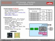
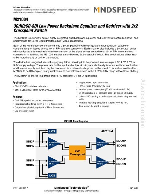
<strong>M21004</strong><br />
3G/HD/SD-SDI Low Power Backplane Equalizer and Redriver with 2x2<br />
Crosspoint Switch<br />
The <strong>M21004</strong> is a very low power, highly integrated, dual backplane equalizer and redriver with optimized power and<br />
performance for Serial Digital Interface (SDI) video applications.<br />
Each of the two independent channels has a 50Ω input buffer with configurable input equalizer, capable of<br />
compensating for losses across 40" of FR4 and two connectors. Each channel also includes a 50Ω output buffer<br />
with configurable de-emphasis to aid transmission of the signal across an additional 40" of FR4 trace and two<br />
connectors. In addition, the <strong>M21004</strong> features a non-blocking 2x2 crosspoint switch. The switch allows either input<br />
to be routed to any or both of the outputs.<br />
The device has integrated internal supply regulators, allowing it to be powered from a single 1.2V, 1.8V, 2.5V, or<br />
3.3V supply voltage. The power rails for the input and output circuitry are electrically independent from each other<br />
and the core supply and thus may be connected to a different voltage rail on the board. This feature enables the<br />
<strong>M21004</strong> to be DC coupled to any upstream and downstream device in the 1.2V to 3.3V range without level shifting.<br />
The <strong>M21004</strong> is offered in a green and RoHS compliant 24-pin QFN package.<br />
Applications<br />
• 3G/HD/SD-SDI switchers and routers<br />
• SMPTE 259, 292M, 344M, 424M, DVB ASI 270Mb/s<br />
Features<br />
• Dual FR4 equalizer and output de-emphasis<br />
• Input equalization for up to 40" of FR4 + 2 connectors<br />
• Output de-emphasis for up to 40" of FR4 + 2 connectors<br />
• 2x2 crosspoint switch<br />
LOS<br />
• Integrated 50Ω input termination<br />
• Loss of Signal detection at the input<br />
• Very low power consumption (50 mW per channel @1.2V)<br />
• On-chip regulators for operation from 1.2V to 3.3V DC supply<br />
• Universal DC coupling at the input and output with integrated level<br />
shifter<br />
• Industrial operating temperature range of -40°C to 85°C<br />
• 4mm x 4mm, 24-pin QFN package<br />
<strong>M21004</strong> Block Diagrams<br />
<strong>M21004</strong><br />
Advance Information<br />
SDI0P<br />
SDI0N<br />
50Ω Buffer<br />
W/ IE<br />
50Ω Buffer<br />
W/ DE<br />
SDO0P<br />
SDO0N<br />
2x2<br />
Crosspoint<br />
SDI1P<br />
SDI1N<br />
50Ω Buffer<br />
W/ IE<br />
50Ω Buffer<br />
W/ DE<br />
SDO1P<br />
SDO1N<br />
LOS<br />
21004-DSH-001-A Mindspeed Technologies ® July 2008<br />
Advance Information / Mindspeed Proprietary and Confidential
Ordering Information<br />
Part Number Package Operating Temperature<br />
<strong>M21004</strong>G-xx* 4 mm, 24-pin QFN (RoHS compliant) –40 °C to 85 °C<br />
* The letter “G” designator after the part number indicates that the device is RoHS compliant. Refer to www.mindspeed.com for additional<br />
information. The RoHS compliant devices are backwards compatible with 225 °C reflow profiles.<br />
Revision History<br />
Revision Level Date Description<br />
A Advance July 2008 Initial Release<br />
Advance Information<br />
21004-DSH-001-A Mindspeed Technologies ® 2<br />
Advance Information / Mindspeed Proprietary and Confidential
Table of Contents<br />
Ordering Information . . . . . . . . . . . . . . . . . . . . . . . . . . . . . . . . . . . . . . . . . . . . . . . . . . . . . . . . . . . . . . . . . . 2<br />
Revision History. . . . . . . . . . . . . . . . . . . . . . . . . . . . . . . . . . . . . . . . . . . . . . . . . . . . . . . . . . . . . . . . . . . . . . 2<br />
Table of Contents. . . . . . . . . . . . . . . . . . . . . . . . . . . . . . . . . . . . . . . . . . . . . . . . . . . . . . . . . . . . . . . . . . . . . 3<br />
1.0 Electrical Characteristics. . . . . . . . . . . . . . . . . . . . . . . . . . . . . . . . . . . . . . . . . . . . . . . . . . . . . . . . . . . 4<br />
2.0 Typical Performance Characteristics. . . . . . . . . . . . . . . . . . . . . . . . . . . . . . . . . . . . . . . . . . . . . . . . . . 7<br />
3.0 Pinout Diagram, Pin Descriptions,<br />
and Packaging Outline Drawing . . . . . . . . . . . . . . . . . . . . . . . . . . . . . . . . . . . . . . . . . . . . . . . . . . . . . 8<br />
3.1 Package Drawings and Surface Mount Details . . . . . . . . . . . . . . . . . . . . . . . . . . . . . . . . . . . . . . . . . . . . . . . . . . . .10<br />
4.0 Functional Description . . . . . . . . . . . . . . . . . . . . . . . . . . . . . . . . . . . . . . . . . . . . . . . . . . . . . . . . . . . 13<br />
4.1 High Speed Input Description . . . . . . . . . . . . . . . . . . . . . . . . . . . . . . . . . . . . . . . . . . . . . . . . . . . . . . . . . . . . . . . . .13<br />
4.2 High-Speed Output Description. . . . . . . . . . . . . . . . . . . . . . . . . . . . . . . . . . . . . . . . . . . . . . . . . . . . . . . . . . . . . . . .15<br />
4.3 Power Supply Description . . . . . . . . . . . . . . . . . . . . . . . . . . . . . . . . . . . . . . . . . . . . . . . . . . . . . . . . . . . . . . . . . . . .16<br />
4.4 Logic Control Signals . . . . . . . . . . . . . . . . . . . . . . . . . . . . . . . . . . . . . . . . . . . . . . . . . . . . . . . . . . . . . . . . . . . . . . .18<br />
4.4.1 Input Equalizer Control. . . . . . . . . . . . . . . . . . . . . . . . . . . . . . . . . . . . . . . . . . . . . . . . . . . . . . . . . . . . . . .18<br />
4.4.2 Output De-emphasis Control . . . . . . . . . . . . . . . . . . . . . . . . . . . . . . . . . . . . . . . . . . . . . . . . . . . . . . . . . .18<br />
4.4.2.1 Output Swing Control. . . . . . . . . . . . . . . . . . . . . . . . . . . . . . . . . . . . . . . . . . . . . . . . . . . . . . .18<br />
Advance Information<br />
21004-DSH-001-A Mindspeed Technologies ® 3<br />
Advance Information / Mindspeed Proprietary and Confidential
1.0 Electrical Characteristics<br />
Unless noted otherwise, specifications in this section apply to nominal power supply, 25 °C ambient temperature, 800 mVpp input data<br />
swing, default output data swing, PRBS 2 15 – 1 test pattern, RL = 50Ω. voltages are referenced to AV SS.<br />
Table 1-1.<br />
Absolute Maximum Ratings<br />
Symbol Parameter Note Minimum Typical Maximum Unit<br />
AV DD Analog Core power supply voltage 1 -0.5 — 1.5 V<br />
AV DD OUT Analog power Output supply voltage 1 -0.5 — 3.6 V<br />
AV DD IN Analog power Input supply voltage 1 -0.5 — 3.6 V<br />
V IN,PCML DC input voltage (PCML) 1 -0.5 — AV DD OUT + 0.5 V<br />
V IN,CMOS DC input voltage (CMOS) 1 -0.5 — AV DD OUT + 0.5 V<br />
T STORE Storage temperature 1 -65 — 150 °C<br />
T JUNC Junction temperature 1 -40 — 125 °C<br />
V ESD,HBM Electrostatic discharge voltage (HBM) 1, 2 — — 4 kV<br />
V ESD,CDM Electrostatic discharge voltage (CDM) 1, 2 — — 500 V<br />
NOTES:<br />
1. Exposure of the device beyond the minimum/maximum limits may cause permanent damage. Limits listed in the above table are stress limits<br />
only, and do not imply functional operation within these limits.<br />
2. HBM and CDM per JEDEC Class 2 (JESD22-A114-B).<br />
Table 1-2.<br />
Recommended Operating Conditions<br />
Advance Information<br />
Symbol Parameter Note Minimum Typical Maximum Unit<br />
AV DD Analog Core supply voltage — 1.14 1.2 1.26 V<br />
AV DD OUT Analog Output supply voltage — 1.14 1.2/1.8/2.5/3.3 3.6 V<br />
AV DD IN Analog Input supply voltage — 1.14 1.2/1.8/2.5/3.3 3.6 V<br />
T Operating temperature 1 -40 — 85 °C<br />
θ JA Junction to ambient thermal resistance 2 — TBD — °C/W<br />
θ JC Junction to case thermal resistance 2 — TBD — °C/W<br />
NOTES:<br />
1. Lower limit is ambient temperature and upper limit is case temperature.<br />
2. Without heatsink and without air flow.<br />
21004-DSH-001-A Mindspeed Technologies ® 4<br />
Advance Information / Mindspeed Proprietary and Confidential
Electrical Characteristics<br />
Table 1-3.<br />
Power Consumption Specifications (Per Channel)<br />
Symbol Parameter Note Minimum Typical Maximum Unit<br />
I DD Core Current consumption 1 — TBD TBD mA<br />
I DD OUT Output Current consumption 1 — TBD TBD mA<br />
P TOTAL Power consumption 1 — 50 TBD mW<br />
I DD Core Current consumption 2 — TBD TBD mA<br />
I DD OUT Output Current consumption 2 TBD TBD mA<br />
P TOTAL Power consumption 2 — TBD TBD mW<br />
I DD Core Current consumption 3 — TBD TBD mA<br />
I DD OUT Output Current consumption 3 TBD TBD mA<br />
P TOTAL Power consumption 3 — TBD TBD mW<br />
I DD Core Current consumption 4 — TBD TBD mA<br />
I DD OUT Output Current consumption 4 — TBD TBD mA<br />
P TOTAL Power consumption 4 — TBD TBD mW<br />
NOTES:<br />
1. AV DD , AV DD OUT = 1.2V and low output swing setting.<br />
2. AV DD , AV DD OUT = 1.2V and med output swing setting.<br />
3. AV DD , AV DD OUT = 1.8V and high output swing setting.<br />
4. AV DD OUT = 3.3V, Regulator Enabled and high output swing setting.<br />
Advance Information<br />
21004-DSH-001-A Mindspeed Technologies ® 5<br />
Advance Information / Mindspeed Proprietary and Confidential
Electrical Characteristics<br />
Table 1-4.<br />
PCML Input/Output Electrical Characteristics<br />
Symbol Parameter Note Minimum Typical Maximum Unit<br />
DR NRZ data rate — 143 — 2970 Mbps<br />
V IN Input sensitivity 1 250 800 1600 mVppd<br />
IE Input equalization — — 6, 4, 0 — dB<br />
R IN Input termination resistance 2 — 50 — Ω<br />
V LOSA LOS level, assert 1 — 100 — mVpp<br />
V LOSD LOS level, deassert 1 — 200 — mVpp<br />
V OUT Single-ended output swing - low 5 480 600 720 mVppd<br />
Single-ended output swing - med 5, 6 640 800 960 mVppd<br />
Single-ended output swing - high 4, 5 960 1200 1440 mVppd<br />
R OUT Output termination resistance 3 — 50 — Ω<br />
DE Output de-emphasis settings 7 — 6, 4, 0 — dB<br />
NOTES:<br />
1. Value specified at the device pins.<br />
2. Internal termination to AV DD IN.<br />
3. Internal termination to AV DD OUT.<br />
4. To achieve high swing; AV DD OUT must be > =1.8V.<br />
5. Measured into 50Ω load.<br />
6. Default output swing level.<br />
7. Measured with 16 ones and 16 zeros pattern.<br />
Table 1-5. Control/Interface Logic Input/Output Characteristics<br />
Symbol Parameter Note Minimum Typical Maximum Unit<br />
V IH Input logic high 0.85 x AV DD OUT — AV DD OUT V<br />
V IF Input logic float 0.25 x AV DD OUT — 0.75 x AV DD OUT V<br />
V IL Input logic low 0 — 0.20 x AV DD OUT V<br />
I IL Input Current logic low 100 — uA<br />
I IH Input Current logic high — — -100 uA<br />
Advance Information<br />
21004-DSH-001-A Mindspeed Technologies ® 6<br />
Advance Information / Mindspeed Proprietary and Confidential
2.0 Typical Performance<br />
Characteristics<br />
TBD<br />
Advance Information<br />
21004-DSH-001-A Mindspeed Technologies ® 7<br />
Advance Information / Mindspeed Proprietary and Confidential
3.0 Pinout Diagram, Pin Descriptions,<br />
and Packaging Outline Drawing<br />
Figure 3-1.<br />
<strong>M21004</strong> Pinout Diagram (Top View)<br />
AVDDIN<br />
24<br />
IE_CTRL0<br />
SWING_CTRL0<br />
LOS/MUTE0<br />
XPT_CTRL0<br />
DE_CTRL0<br />
SDI0P 1<br />
SDI0N 2<br />
AV DD 0 3<br />
AV DD 1 4<br />
SDI1P 5<br />
23<br />
22<br />
21<br />
20<br />
<strong>M21004</strong><br />
24 pin<br />
4mmx4mm<br />
QFN<br />
19<br />
18<br />
17<br />
16<br />
15<br />
14<br />
SDO0P<br />
SDO0N<br />
AV DD OUT<br />
SWING_CTRL1<br />
SDO1P<br />
Advance Information<br />
SDI1N 6<br />
13<br />
SDO1N<br />
AV DD IN 7<br />
IE_CTRL1 8<br />
DE_CTRL1 9<br />
LOS/MUTE1 10<br />
xREG_EN 11<br />
XPT_CTRL1 12<br />
Center Ground Pad<br />
21004-DSH-001-A Mindspeed Technologies ® 8<br />
Advance Information / Mindspeed Proprietary and Confidential
Pinout Diagram, Pin Descriptions, and Packaging Outline Drawing<br />
Table 3-1.<br />
<strong>M21004</strong> Pin Descriptions<br />
Pin Name Pin Number(s) Type Description<br />
AV SS Center Pad Power Ground<br />
AV DD 0 3 Power Analog Core positive supply for channel 0<br />
AV DD 1 4 Power Analog Core positive supply for channel 1<br />
AV DD OUT 16 Power Analog positive supply for output circuitry<br />
AV DD IN 24, 7 Power Analog positive supply for input circuitry<br />
xREG_EN 11 I–Digital Internal regulator disable<br />
L = Enable integrated regulator<br />
H = disable integrated regulator<br />
XPT_CTRL[1:0] 12, 20 I–Digital Input Crosspoint Control<br />
L L = Broadcast SDI0; SDI0 to SDO0, SDI0 to SDO1<br />
L H= Crossover; SDI1 to SDO0, SDI0 to SDO1<br />
H L = Feedthrough; SDI0 to SDO0, SDI1 to SDI1 (default)<br />
H H = Broadcast SDI1; SDI1 to SDO0, SDI1 to SDI1<br />
SWING_CTRL0, 1 22, 15 3-state/<br />
I–Digital<br />
Output swing control for channel 0 and channel 1<br />
L = low<br />
F = med(default)<br />
H = high<br />
DE_CTRL0, 1 19, 9 3-state/<br />
I–Digital<br />
Output de-emphasis control for channel 0 and channel 1<br />
L = DE off<br />
F = Medium DE (default)<br />
H = High DE<br />
IE_CTRL0, 1 23, 8 3-state/<br />
I–Digital<br />
Input Equalization control for channel 0 and channel 1<br />
L = IE off<br />
F = Medium IE (default)<br />
H = High IE<br />
LOS/MUTE0, 1 21, 10 O-Digital/<br />
I–Digital<br />
Configured as output (> 50 kΩ resistive load):<br />
LOS alarm output (active high) for channel 0 and channel 1<br />
Configured as input (driven with R < 0.25 kΩ)<br />
L = never mute the output<br />
H = force mute the output<br />
SDI0P 1 I-Analog Serial <strong>Data</strong> video input0, true<br />
SDI0N 2 I-Analog Serial <strong>Data</strong> video input0, complement<br />
SDI1P 5 I-Analog Serial <strong>Data</strong> video input1, true<br />
SDI1N 6 I-Analog Serial <strong>Data</strong> video input1, complement<br />
SDO0P 18 O-Analog Serial <strong>Data</strong> output0, true<br />
SDO0N 17 O-Analog Serial <strong>Data</strong> output0, complement<br />
SDO1P 14 O-Analog Serial <strong>Data</strong> output1, true<br />
SDO1N 13 O-Analog Serial <strong>Data</strong> output1, complement<br />
Advance Information<br />
21004-DSH-001-A Mindspeed Technologies ® 9<br />
Advance Information / Mindspeed Proprietary and Confidential
Pinout Diagram, Pin Descriptions, and Packaging Outline Drawing<br />
3.1 Package Drawings and Surface Mount Details<br />
The <strong>M21004</strong> is assembled in a 24-pin, 4 mm x 4 mm Quad Flat No-Lead (QFN) package. The exposed die paddle<br />
serves as the IC ground (AV SS ), and the primary means of thermal dissipation. This die paddle should be soldered<br />
to the PCB ground. A cross-section of the QFN package can be found in Figure 3-2.<br />
Figure 3-2.<br />
QFN Package Cross Section<br />
Mold Compound<br />
Ag Plating<br />
Solder<br />
Plating<br />
Die<br />
Gold Wire<br />
Cu Leadframe<br />
Down Bond<br />
Exposed Die<br />
Paddle<br />
Ground Bond<br />
Die Attach Material<br />
Advance Information<br />
21004-DSH-001-A Mindspeed Technologies ® 10<br />
Advance Information / Mindspeed Proprietary and Confidential
Pinout Diagram, Pin Descriptions, and Packaging Outline Drawing<br />
Figure 3-3.<br />
<strong>M21004</strong> Package Drawing<br />
Advance Information<br />
21004-DSH-001-A Mindspeed Technologies ® 11<br />
Advance Information / Mindspeed Proprietary and Confidential
Pinout Diagram, Pin Descriptions, and Packaging Outline Drawing<br />
Figure 3-4.<br />
<strong>M21004</strong> 24-Pin Package Dimensions<br />
Advance Information<br />
21004-DSH-001-A Mindspeed Technologies ® 12<br />
Advance Information / Mindspeed Proprietary and Confidential
4.0 Functional Description<br />
Figure 4-1 illustrates the functional block diagram of the <strong>M21004</strong>. The subsequent sections provide additional<br />
detail on the operation of the device.<br />
Figure 4-1.<br />
<strong>M21004</strong> Functional Block Diagram<br />
LOS0<br />
AVDD0<br />
AVDD1<br />
AVDDOUT<br />
SDI0P<br />
SDI0N<br />
SDI0P<br />
SDI0N<br />
LOS<br />
LOS<br />
50Ω<br />
Buffer w/<br />
IE<br />
50Ω<br />
Buffer w/<br />
IE<br />
Regulator<br />
2X2<br />
Xpoint<br />
Control Logic<br />
50Ω<br />
Buffer w/<br />
DE<br />
50Ω<br />
Buffer w/<br />
DE<br />
SDO0P<br />
SDO0N<br />
SDO1P<br />
SDO1N<br />
Advance Information<br />
LO S1<br />
IE_CTRL0<br />
IE_CTRL1<br />
DE_CTRL0<br />
DE_CTRL1<br />
XPT_CTRL0<br />
XPT_CTRL1<br />
LO S/MUTE0<br />
LO S/MUTE1<br />
SWING_CTRL0<br />
SWING_CTRL1<br />
xREG_EN<br />
AV DD IN<br />
4.1 High Speed Input Description<br />
The <strong>M21004</strong> features two inputs with a 50Ω termination to AV DD IN. AV DD IN can be supplied from any voltage<br />
ranging from 1.2V to 3.3V.<br />
In order to improve signal integrity when used in large systems, each input also comes equipped with<br />
programmable input equalization (IE) for FR4 trace. There are three settings for input equalization: 6 dB, 4 dB and<br />
21004-DSH-001-A Mindspeed Technologies ® 13<br />
Advance Information / Mindspeed Proprietary and Confidential
Functional Description<br />
0 dB (or no equalization). The IE for each input channel is controlled through the corresponding three state control<br />
pin: IE_CTRL0 or IE_CTRL1.<br />
In most SDI applications, it is important to avoid AC coupled data interfaces between devices wherever possible. In<br />
addition to reducing the number of components, DC coupling will result in more system jitter margin. In order to<br />
accommodate DC coupling with the upstream device, the AV DD IN power domain of the <strong>M21004</strong> is electrically<br />
independent from all other power domains allowing it to be tied to the VDD of the upstream device. This is<br />
demonstrated in Figure 4-2 below.<br />
Figure 4-2. <strong>M21004</strong> AV DD IN Connected to the VDD of the Upstream Device<br />
Upstream<br />
50Ω<br />
VDD<br />
1.2V – 3.3V<br />
AV DD IN<br />
50Ω<br />
<strong>M21004</strong><br />
Alternatively and provided that the internal regulators are not used, the <strong>M21004</strong> allows for the input to be self<br />
biased, eliminating the need for an electrical connection between the supply voltages of the upstream device and<br />
<strong>M21004</strong>. This configuration offers the benefit of keeping the supply of the previous device and the power domain(s)<br />
of the <strong>M21004</strong> completely isolated, while still allowing DC coupling. This self biasing scheme is demonstrated in<br />
Figure 4-3 below.<br />
Figure 4-3. Self Biasing the Input of <strong>M21004</strong><br />
Upstream<br />
VDD<br />
50Ω<br />
0.1uF<br />
<strong>M21004</strong><br />
AV DD IN<br />
50Ω<br />
Advance Information<br />
In this configuration, the minimum input common mode that can be tolerated is 600 mV. If AC coupling is desired or<br />
necessary, then the capacitor should be at least 4.7 uF for SDI applications.<br />
21004-DSH-001-A Mindspeed Technologies ® 14<br />
Advance Information / Mindspeed Proprietary and Confidential
Functional Description<br />
<br />
A Loss of Signal (LOS) detector monitors each input and issues an alarm when the input signal level dips below the<br />
detection threshold of 200 mVppd. A hysteresis of +100 mV has been implemented, to avoid chattering of the<br />
xALARM pin.<br />
By default, the LOS alarm mutes the signal of that particular input. The LOS pin maybe overridden with an external<br />
signal to prevent muting of the output.<br />
4.2 High-Speed Output Description<br />
The <strong>M21004</strong> features differential positive current mode logic (PCML) drivers with integrated 50Ω pull ups to<br />
AV DD OUT. AV DD OUT may be supplied from any voltage ranging from 1.2V to 3.3V.<br />
The differential, peak-to-peak output swing for each PCML driver is selectable and may be set to low, med, or high<br />
through the SWING_CTRL pin. Please note that the high output swing setting is only available when AV DD OUT is<br />
supplied from a voltage of 1.8V or greater.<br />
In order to improve signal integrity when used in large systems, each output also comes equipped with<br />
programmable de-emphasis (DE) for FR4 trace. There are three settings for output de-emphasis: 0 dB (or no DE),<br />
4 dB, and 6 dB. The de-emphasis level for each output is set through the DE_CTRL0 and DE_CTRL1 pins.<br />
In most SDI applications, it is important to avoid AC coupled data interfaces between devices wherever possible. In<br />
addition to reducing the number of components, DCcoupling will result in more system jitter margin. In order to<br />
accommodate DC coupling with the downstream device, the AV DD OUT power domain of the <strong>M21004</strong> is electrically<br />
independent from all other power domains, therefore allowing it to be tied to the VDD of the downstream device.<br />
This is demonstrated in Figure 4-4 below.<br />
Figure 4-4. <strong>M21004</strong> AV DD OUT Connected to the VDD of the Downstream Device<br />
<strong>M21004</strong><br />
AV DD OUT<br />
50<br />
1.2V –<br />
VDD<br />
Downstream<br />
50<br />
Advance Information<br />
If AC coupling is desired or necessary, then the capacitor should be at least 4.7 uF.<br />
21004-DSH-001-A Mindspeed Technologies ® 15<br />
Advance Information / Mindspeed Proprietary and Confidential
Functional Description<br />
4.3 Power Supply Description<br />
The device core is designed to operate from a nominal 1.2V supply. However, if a 1.2V supply is not available<br />
locally then the internal regulator can be used to create a 1.2V domain from AV DD OUT.<br />
Note that as AV DD IN is electrically independent, it must always be supplied with a voltage within the specified range<br />
regardless of whether the regulator is enabled or not.<br />
The regulator is controlled through the active low xREG_EN pin. Setting the pin LOW by connecting it to AV SS<br />
enables the regulator. The xREG_EN signal is referenced to AV DD OUT, so in order to set it HIGH it must be<br />
connected to that supply rail. However, the pin features an integrated pull-up resistor, so it may be left floating if the<br />
regulator is not used.<br />
The total power consumption of the device will increase when the internal regulator is enabled.<br />
Figure 4-5 to Figure 4-8 illustrate the connection for four different supply configurations. Note that the decoupling<br />
capacitors must be 0.1 uF or greater.<br />
Figure 4-5. Supply Configuration Example #1<br />
0.1µF<br />
AV DDIN<br />
AV DDIN<br />
xREG_EN<br />
1.2V<br />
<strong>M21004</strong><br />
AV DDOUT<br />
AV DD0<br />
AV DD1<br />
0.1µF<br />
0.1µF<br />
1.2V Supply Only<br />
Both channels used, internal regulators are not used<br />
0.1µF<br />
Advance Information<br />
21004-DSH-001-A Mindspeed Technologies ® 16<br />
Advance Information / Mindspeed Proprietary and Confidential
Functional Description<br />
Figure 4-6. Supply Configuration Example #2<br />
1.2/1.8/2.5/3.3V<br />
1.2/1.8/2.5/3.3V<br />
AV DDIN<br />
AV DDIN<br />
<strong>M21004</strong><br />
AV DDOUT<br />
AV DD0<br />
1.2V<br />
0.1µF<br />
xREG_EN<br />
AV DD1<br />
0.1µF<br />
0.1µF<br />
0.1µF<br />
1.2V used for Core, 1.8V/2.5V/3.3V used for Input and Output<br />
Both channels used, internal regulators are not used<br />
Figure 4-7. Supply Configuration Example #3<br />
1.2/1.8/2.5/3.3V<br />
0.1µF<br />
AV DDIN<br />
AV DDIN<br />
xREG_EN<br />
<strong>M21004</strong><br />
AV DDOUT<br />
AV DD0<br />
AV DD1<br />
1.2/1.8/2.5/3.3V<br />
1.2V<br />
0.1µF<br />
1.2V used for Core, 1.8V/2.5V/3.3V used for Input and Output<br />
Channel 1 not used, internal regulators are not used<br />
0.1µF<br />
Advance Information<br />
Figure 4-8. Supply Configuration Example #4<br />
1.2/1.8/2.5/3.3V<br />
1.8/2.5/3.3V<br />
AV DDIN<br />
AV DDOUT<br />
AV DDIN<br />
<strong>M21004</strong><br />
AV DD0<br />
0.1µF<br />
xREG_EN<br />
AV DD1<br />
0.1µF<br />
0.1µF<br />
0.1µF<br />
1.8V/2.5V/3.3V used for Core, Input and Output<br />
Both channels used, internal regulators are used for Core<br />
21004-DSH-001-A Mindspeed Technologies ® 17<br />
Advance Information / Mindspeed Proprietary and Confidential
Functional Description<br />
4.4 Logic Control Signals<br />
The <strong>M21004</strong> may be configured through several digital control pins. In order to allow interfacing to logic levels other<br />
than the 1.2V core voltage, the digital control signals are referenced to AV DD OUT.<br />
Some digital control pins have three states: HIGH (H), LOW (L), or FLOATING (F). In order to assert the F state,<br />
the pin must be left unconnected or undriven.<br />
4.4.1 Input Equalizer Control<br />
The IE_CTRL pins in the <strong>M21004</strong> set the equalizer level for the corresponding inputs.<br />
Table 4-1.<br />
Operation of IE_CTRL Pins (Input Equalizer)<br />
Pin Level Function<br />
L Input equalization disabled<br />
IE_CTRL0,<br />
IE_CTRL1<br />
F Med equalization (default)<br />
H High equalization<br />
4.4.2 Output De-emphasis Control<br />
The DE_CTRL pins in the <strong>M21004</strong> set the de-emphasis level for the corresponding outputs.<br />
Table 4-2. Operation of DE_CTRL Pins (De-emphasis)<br />
Pin Level Function<br />
L De-emphasis disabled<br />
DE_CTRL0,<br />
DE_CTRL1<br />
F Med de-emphasis (default)<br />
H High de-emphasis<br />
4.4.2.1 Output Swing Control<br />
The SWING_CTRL pin in the <strong>M21004</strong> sets the PCML swing level for the corresponding output.<br />
Advance Information<br />
Table 4-3.<br />
Operation of SWING_CTRL Pin<br />
Pin Level Function<br />
SWING_CTRL0,<br />
SWING_CTRL1<br />
L<br />
F<br />
H<br />
Output swing set to low<br />
Output swing set to med (default)<br />
Output swing set to high<br />
21004-DSH-001-A Mindspeed Technologies ® 18<br />
Advance Information / Mindspeed Proprietary and Confidential
www.mindspeed.com<br />
General Information:<br />
Telephone: (949) 579-3000<br />
Headquarters - Newport Beach<br />
4000 MacArthur Blvd., East Tower<br />
Newport Beach, CA 92660<br />
© 2009 Mindspeed Technologies ® , Inc. All rights reserved.<br />
Information in this document is provided in connection with Mindspeed Technologies ® ("Mindspeed ® ") products.<br />
These materials are provided by Mindspeed as a service to its customers and may be used for informational<br />
purposes only. Except as provided in Mindspeed’s Terms and Conditions of Sale for such products or in any<br />
separate agreement related to this document, Mindspeed assumes no liability whatsoever. Mindspeed assumes<br />
no responsibility for errors or omissions in these materials. Mindspeed may make changes to specifications and<br />
product descriptions at any time, without notice. Mindspeed makes no commitment to update the information and<br />
shall have no responsibility whatsoever for conflicts or incompatibilities arising from future changes to its<br />
specifications and product descriptions. No license, express or implied, by estoppel or otherwise, to any<br />
intellectual property rights is granted by this document.<br />
THESE MATERIALS ARE PROVIDED "AS IS" WITHOUT WARRANTY OF ANY KIND, EITHER EXPRESS OR<br />
IMPLIED, RELATING TO SALE AND/OR USE OF <strong>MINDSPEED</strong> PRODUCTS INCLUDING LIABILITY OR<br />
WARRANTIES RELATING TO FITNESS FOR A PARTICULAR PURPOSE, CONSEQUENTIAL OR INCIDENTAL<br />
DAMAGES, MERCHANTABILITY, OR INFRINGEMENT OF ANY PATENT, COPYRIGHT OR OTHER<br />
INTELLECTUAL PROPERTY RIGHT. <strong>MINDSPEED</strong> FURTHER DOES NOT WARRANT THE ACCURACY OR<br />
COMPLETENESS OF THE INFORMATION, TEXT, GRAPHICS OR OTHER ITEMS CONTAINED WITHIN THESE<br />
MATERIALS. <strong>MINDSPEED</strong> SHALL NOT BE LIABLE FOR ANY SPECIAL, INDIRECT, INCIDENTAL, OR<br />
CONSEQUENTIAL DAMAGES, INCLUDING WITHOUT LIMITATION, LOST REVENUES OR LOST PROFITS,<br />
WHICH MAY RESULT FROM THE USE OF THESE MATERIALS.<br />
Mindspeed products are not intended for use in medical, lifesaving or life sustaining applications. Mindspeed<br />
customers using or selling Mindspeed products for use in such applications do so at their own risk and agree to<br />
fully indemnify Mindspeed for any damages resulting from such improper use or sale.<br />
Advance Information<br />
21004-DSH-001-A Mindspeed Technologies ® 19<br />
Advance Information / Mindspeed Proprietary and Confidential