CX20662 App Note 1 - PCB Layout Guidelines APN ... - Codico
CX20662 App Note 1 - PCB Layout Guidelines APN ... - Codico
CX20662 App Note 1 - PCB Layout Guidelines APN ... - Codico

Create successful ePaper yourself
Turn your PDF publications into a flip-book with our unique Google optimized e-Paper software.
<strong>CX20662</strong> <strong>PCB</strong> <strong>Layout</strong> <strong>Guidelines</strong><br />
Revision 1.0<br />
November 24, 2008<br />
These layout guidelines reference component and net names from the Conexant CX-9Z-NR0340-00-1.X reference<br />
design. It is recommended to have the CX-9Z-NR0340-00-1.X schematic and G600Z-NR0340-00-1.0 Allegro<br />
layout files available while reading this document.<br />
Component Placement<br />
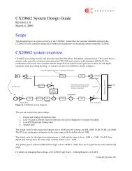
<strong>CX20662</strong> Analog<br />
Component placement guidelines are listed below in order of priority. Analog signals have priority over digital<br />
signals. The <strong>CX20662</strong> device should be oriented such that the analog signals are as short as possible. Analog and<br />
digital sections should be separated as much as possible.<br />
1. Place microphone circuit (J12, R406, C401, R42, C218) as close to U4 as possible.<br />
2. Place speaker circuit (J10, J405, C25, C34, C36, C200-C201, R200-R201, L20-L21, and R10, R11) as<br />
close to U4 as possible.<br />
3. Place headphone circuit (J404, C49, R44, R432, C216) as close to U4 as possible.<br />
4. Place volume control circuit (R29, R54, C27, C31) close to U4, pin 14.<br />
<strong>CX20662</strong> Digital<br />
Component placement guidelines are listed below in order of priority.<br />
1. Current sense resistor, R428, must be placed as close as possible to U4. It is critical that the traces<br />
from R428 to U4 be as short and wide as possible to minimize trace impedance. R428 is used to sense<br />
an overcurrent event and large trace impedances will affect the overcurrent trigger point.<br />
2. Place crystal circuit as close to U4, pins 6 and 7 as possible.<br />
3. Place decoupling caps (C8-C14, C21) as close to the appropriate pins on U4 as possible.<br />
4. Place remaining digital components in such a way as to minimize trace lengths.<br />
DAA<br />
The DAA circuit is shown on page 4 of the schematic. All components to the right of T1 need to be placed inside a<br />
3mm isolation barrier. See G600Z-NR0340-00-1.0 Allegro layout file for an example. Components to the left of T1<br />
should be placed near T1.<br />
1<br />
Conexant Systems, Inc.
Critical Trace Widths, Lengths, and Clearances<br />
Analog<br />
The following signals should be routed as differential pairs and shielded from other signals by GND. No GND<br />
between the differential pair. Trace width shall be 20 mils, spacing between differential pair signals shall be 10<br />
mils, and spacing to AGND shield shall be 15 mils. Trace lengths shall be as short as possible. These signals are<br />
the most critical in this design.<br />
• SPK+/-, SPK1+/-, SPK2+/-<br />
The following signals should be shielded from other signals by GND. Trace width shall be 20 mils and spacing to<br />
AGND shield shall be 10 mils. Trace lengths shall be as short as possible. These signals are the most critical in this<br />
design.<br />
• MIC_MONO, MIC_MONO2 and MICBIAS<br />
• HP_MONO, HP_MONO2, HP_MONO3<br />
Analog power traces shall be routed as 25-mil wide traces. The analog power nets are listed below.<br />
• +5V_CLASSD<br />
• +3.3VA<br />
• +1.65_VREF<br />
• +2.5_VREFD<br />
Digital<br />
Crystal traces should be 12 mils wide with 12 mil spacing.<br />
Digital power traces shall be routed as 25-mil wide traces. The digital power nets are listed below.<br />
DAA<br />
• +5V<br />
• +5V_REG<br />
• BRICK_IN<br />
• +1.8V_VCORE<br />
• +3.3VD<br />
Traces from J5 to RV1 should be 25 mils thick with 25 mil spacing.<br />
All other DAA traces should be 15 mils thick with 20 mil spacing.<br />
2<br />
Conexant Systems, Inc.
Power and Ground<br />
There shall be a single ground plane on the board. Try to route most of the signals on layer 1 so that layer 2 can be a<br />
solid ground plane.<br />
Power traces shall be routed as 25-mil wide traces.<br />
Silkscreen<br />
All component reference designators need to be shown in silkscreen. Avoid placing silkscreen on top of vias. It is<br />
recommended to also label the following:<br />
Label SW34: Volume Down<br />
Label SW36: Volume Up<br />
Label SW29: Mic Mute<br />
Label SW35: Spkr Mute<br />
Label J14: UART<br />
Label JP3: NVCLK<br />
Label JP4: NVDATA<br />
Label D2: Power LED<br />
Label D6: Mic Mute LED<br />
Label 17: Spkr Mute LED<br />
Label J10, pin 1: Spkr +<br />
Label J10, pin 2: Spkr –<br />
Label J12, pin 1: GND<br />
Label J12, pin 2: MIC<br />
Label J405: Mono Speaker<br />
Label J404: Headset Jack<br />
Label R29: Analog Volume<br />
Label JP8: Headphone Sense<br />
Label JP9/SW1: Speakerphone Enable<br />
Label JP5/SW2: OFF-HOOK<br />
Label JP3/JP4: DC Loop<br />
3<br />
Conexant Systems, Inc.
Test Points and Manufacturing Rules<br />
The table below summarizes typical manufacturing recommendations.<br />
Parameter<br />
Value<br />
Test Point Shape<br />
Square<br />
Test Point Minimum size/diameter 35<br />
Minimum spacing between TPs (center-center) 75<br />
Minimum spacing between TP and component pin (center-center) 75<br />
Minimum spacing between TP and board edge (edge-edge) 100<br />
Smallest allowed component size 0603<br />
Minimum trace clearance from edge of board (edge-edge) 40<br />
Minimum thru-hole component body clearance from edge of board<br />
40<br />
(edge-edge)<br />
Minimum surface mount component and thru-hole pad clearance from 115<br />
edge of board (edge-edge)<br />
Minimum spacing between via and pad 8<br />
Minimum spacing between any 2 components (edge-edge) 15<br />
<strong>Note</strong> 1: All dimensions in mils.<br />
<strong>Note</strong> 2: All test points should be placed on one side of the board. 100% test point coverage desired.<br />
Fab <strong>Note</strong>s<br />
See Conexant G600Z-NR0340-00 Allegro .BRD file for fab notes example.<br />
Fiducial Marks<br />
Place 3 fiducial marks on each layer where components are placed.<br />
4<br />
Conexant Systems, Inc.