EB205 Motorola GaAs Rectifiers Offer High Efficiency in a 1 ... - ECA
EB205 Motorola GaAs Rectifiers Offer High Efficiency in a 1 ... - ECA
EB205 Motorola GaAs Rectifiers Offer High Efficiency in a 1 ... - ECA

You also want an ePaper? Increase the reach of your titles
YUMPU automatically turns print PDFs into web optimized ePapers that Google loves.
SEMICONDUCTOR ENGINEERING BULLETIN<br />
Order this document<br />
by <strong>EB205</strong>/D<br />
<br />
<br />
By Scott Deuty<br />
<strong>Motorola</strong> Inc.<br />
<br />
Efficient power conversion circuitry requires rectifiers that<br />
exhibit low forward voltage drop, low reverse recovery current,<br />
and fast recovery time. Silicon has been the material of choice<br />
for fast, efficient rectification <strong>in</strong> switched power applications.<br />
However, technology is near<strong>in</strong>g the theoretical limit for<br />
optimiz<strong>in</strong>g reverse recovery <strong>in</strong> silicon devices. A new material<br />
is required to <strong>in</strong>crease switch<strong>in</strong>g speed.<br />
To <strong>in</strong>crease speed, materials with faster carrier mobility are<br />
needed. Gallium Arsenide (<strong>GaAs</strong>) has a carrier mobility which<br />
is five times that of silicon [1]. S<strong>in</strong>ce Schottky technology for<br />
silicon devices is difficult to produce at voltages above 200 V,<br />
development has focused on <strong>GaAs</strong> devices with rat<strong>in</strong>gs of<br />
180 V and higher. The advantages realized by us<strong>in</strong>g <strong>GaAs</strong><br />
rectifiers <strong>in</strong>clude fast switch<strong>in</strong>g and reduced reverse recovery<br />
related parameters. An additional benefit is the variation of<br />
parameters with temperature is much less than Silicon based<br />
rectifiers.<br />
<strong>Motorola</strong>’s 180 V and 250 V <strong>GaAs</strong> rectifiers are be<strong>in</strong>g used<br />
<strong>in</strong> power converters that produce 24, 36 and even 48 Vdc<br />
outputs. Converters produc<strong>in</strong>g 48 Vdc are especially popular<br />
<strong>in</strong> telecommunications and ma<strong>in</strong>frame computer applications.<br />
To show the advantages of the <strong>GaAs</strong> parts, a 48 Volt DC–DC<br />
converter was constructed and the performance of the <strong>GaAs</strong><br />
rectifiers was compared to similar silicon–based parts at a<br />
switch<strong>in</strong>g frequency of 1 MHz. An output power level of<br />
450 watts was chosen to profile the MGR1018 near its 8 amp<br />
current rat<strong>in</strong>g. The converter was tested with an <strong>in</strong>put voltage<br />
level of 400 volts to simulate the commonly used rail produced<br />
by Power Factor Correction boost converters.<br />
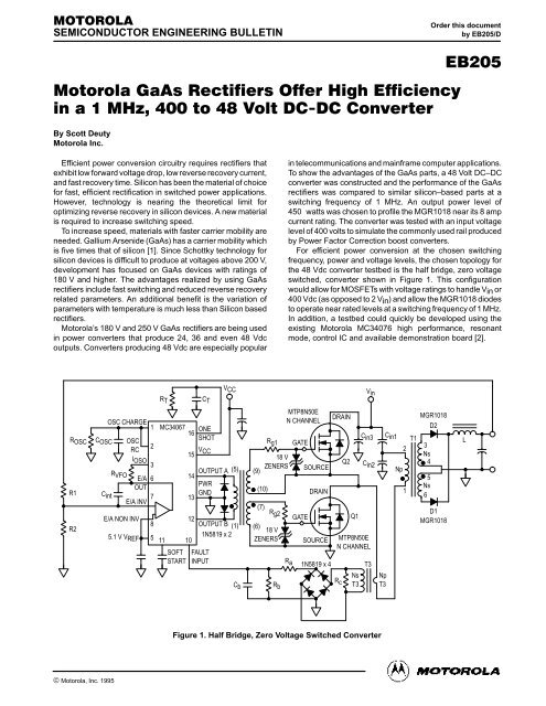
For efficient power conversion at the chosen switch<strong>in</strong>g<br />
frequency, power and voltage levels, the chosen topology for<br />
the 48 Vdc converter testbed is the half bridge, zero voltage<br />
switched, converter shown <strong>in</strong> Figure 1. This configuration<br />
would allow for MOSFETs with voltage rat<strong>in</strong>gs to handle V<strong>in</strong> or<br />
400 Vdc (as opposed to 2 V<strong>in</strong>) and allow the MGR1018 diodes<br />
to operate near rated levels at a switch<strong>in</strong>g frequency of 1 MHz.<br />
In addition, a testbed could quickly be developed us<strong>in</strong>g the<br />
exist<strong>in</strong>g <strong>Motorola</strong> MC34076 high performance, resonant<br />
mode, control IC and available demonstration board [2].<br />
RT<br />
CT<br />
VCC<br />
V<strong>in</strong><br />
ROSC<br />
R1<br />
R2<br />
OSC CHARGE<br />
1<br />
COSC OSC<br />
RC<br />
2<br />
IOSO<br />
3<br />
RVFO<br />
E/A 6<br />
OUT<br />
C<strong>in</strong>t<br />
E/A INV<br />
7<br />
E/A NON INV<br />
5.1 V VREF<br />
8<br />
5<br />
MC34067<br />
16<br />
11<br />
SOFT<br />
START<br />
ONE<br />
SHOT<br />
15<br />
VCC<br />
OUTPUT A (5)<br />
14<br />
PWR<br />
GND<br />
13<br />
12<br />
OUTPUT B (1)<br />
10<br />
1N5819 x 2<br />
FAULT<br />
INPUT<br />
Cb<br />
(9)<br />
(10)<br />
(7)<br />
Rg1<br />
18 V<br />
ZENERS<br />
Rg2<br />
(6)<br />
18 V<br />
ZENERS<br />
Rb<br />
MTP8N50E<br />
N CHANNEL<br />
Ra<br />
GATE<br />
GATE<br />
SOURCE<br />
DRAIN<br />
SOURCE<br />
1N5819 x 4<br />
DRAIN<br />
Q2<br />
Q1<br />
MTP8N50E<br />
N CHANNEL<br />
Rc<br />
Ns<br />
T3<br />
C<strong>in</strong>3<br />
C<strong>in</strong>2<br />
T3<br />
Np<br />
T3<br />
C<strong>in</strong>1<br />
Np<br />
2<br />
1<br />
MGR1018<br />
D2<br />
T1<br />
3<br />
Ns<br />
4<br />
5<br />
Ns<br />
6<br />
D1<br />
MGR1018<br />
L<br />
Figure 1. Half Bridge, Zero Voltage Switched Converter<br />
© MOTOROLA<br />
<strong>Motorola</strong>, Inc. 1995<br />
1
<strong>GaAs</strong> PERFORMANCE RESULTS<br />
Performance results for output power levels of 73 watts to<br />
460 watts are presented <strong>in</strong> Figures 2 through 5 and Tables 2<br />
and 3.<br />
In Table 1, shows how 10 amp, MGR1018 <strong>GaAs</strong> rectifiers<br />
offer an advantage over silicon parts with a 20 amp current<br />
rat<strong>in</strong>g. (Note: only one side of the silicon device was used<br />
for equal comparison.) The efficiency ga<strong>in</strong>s of the <strong>GaAs</strong><br />
rectifiers decrease with output power somewhat due to its<br />
larger forward voltage drop. However, the silicon devices<br />
did not perform above 143 watts. This was attributed to the<br />
large amount of r<strong>in</strong>g<strong>in</strong>g due the large reverse recovery peak<br />
exhibited by the silicon devices. The peak current<br />
generated a high voltage spike that <strong>in</strong> turn forced the<br />
MBR20200 <strong>in</strong>to a zener mode and destroyed the part.<br />
Figure 2 shows the efficiency achieved from the<br />
converter over a power output of 96 to 460 watts. The<br />
switch<strong>in</strong>g frequency of the <strong>in</strong>ductor was 1.2 MHz throughout<br />
this power range. Through use of zero voltage switch<strong>in</strong>g by<br />
the MC34067 IC and the fast recovery times of the rectifiers,<br />
the converter was able to achieve efficiencies <strong>in</strong> excess of<br />
91% with a maximum of 95.4%! Note that the <strong>in</strong>crease <strong>in</strong><br />
<strong>GaAs</strong> efficiency <strong>in</strong> Figure 2 over Table 1 is due to the use of<br />
both leads of the MGR1018 part <strong>in</strong> Figure 2. In Table 1, one<br />
outer lead is connected on the s<strong>in</strong>gle die MGR10180 (each<br />
outer leg is attached to the s<strong>in</strong>gle die) and only one outer<br />
lead is connected on the dual die MBR20200. This allows<br />
for comparison of a silicon MBR20200, die rated at 10 amps<br />
(one half of device) to a 10 amp rated MGR1018. After<br />
runn<strong>in</strong>g the silicon comparison, both outer leads of the test<br />
socket were connected for maximum efficiency realized <strong>in</strong><br />
Figure 2.<br />
Table 1. Performance Benefits Realized<br />
When Us<strong>in</strong>g <strong>GaAs</strong> versus Silicon <strong>Rectifiers</strong><br />
(400 Volts Input, 1.1 to 1.29 MHz Converter Frequency)<br />
Output<br />
Power<br />
Center Tap<br />
Si<br />
MBR20200<br />
<strong>Efficiency</strong><br />
S<strong>in</strong>gle<br />
<strong>GaAs</strong><br />
MGR1018<br />
<strong>Efficiency</strong><br />
<strong>GaAs</strong><br />
Advantage<br />
73 Watts 81.6% 84.2% 2.6%<br />
95 Watts 87.2% 91.2% 3.9%<br />
119 Watts 91.4% 91.9% 0.5%<br />
143 Watts 92.7% 92.7% 0.0%<br />
96<br />
MGR1018 <strong>Efficiency</strong> and Regulation at 375 Vdc Input Level<br />
95.5<br />
95.4%<br />
95<br />
94.5<br />
94.5%<br />
EFFICIENCY (%)<br />
94<br />
93.5<br />
93<br />
92.5<br />
92<br />
91.5<br />
91<br />
96 119 143 166 189 237 264 287 309 343 380 427 449 455 462<br />
OUTPUT POWER (WATTS)<br />
Figure 2. <strong>GaAs</strong> <strong>Offer</strong>s <strong>High</strong> <strong>Efficiency</strong> at<br />
Switch<strong>in</strong>g Frequencies Above 1 MHz<br />
(Input Voltage Rang<strong>in</strong>g from 375 Vdc to 405 Vdc)<br />
2 MOTOROLA
Component<br />
Table 2. Parts List<br />
Reference<br />
Designator Part Value 1 Value 2<br />
Transformer T1 Core<br />
Ma<strong>in</strong> Power Path (Bolded on Schematic)<br />
Magnetics Inc. (1)<br />
K 43515–EC<br />
Transformer T1 Primary Turns: Np = 46<br />
Transformer T1 Secondary Turns: Ns = 13<br />
Inductor L Core Magnetics Inc. 55121–A2<br />
Inductor L W<strong>in</strong>d<strong>in</strong>gs Turns: NL = 12<br />
<br />
Wire:<br />
1–180 strand, #44 AWG<br />
Litz (2)<br />
Wire:<br />
1–1000 strand, #48 AWG<br />
Litz (2)<br />
Wire:<br />
1–175 strand, #38 AWG<br />
Litz (2)<br />
Transistors Q1 & Q2 MTP8N50E 8 Amp 500 V<br />
<strong>Rectifiers</strong> D1 & D2 MGR1018 10 Amp 180 V<br />
Output Capacitors (3)<br />
Input Voltage Divider<br />
Capacitors<br />
Cout<br />
T491X685M050AS<br />
(Qty 6)<br />
6–6.8 µF 50 V<br />
C<strong>in</strong>1 & C<strong>in</strong>2 polypropylene 4–0.1 µF 400 Vdc, 250 Vac<br />
Input Capacitor C<strong>in</strong>3 ceramic 0.01 µF 400 V<br />
Gate Drive<br />
Transformer T3 Core Magnetics Inc. K EP7<br />
Transformer T3 All W<strong>in</strong>d<strong>in</strong>gs Turns: 8 #38 AWG Magnet<br />
Resistors Rg1 & Rg2 film resistor 5.2 Ω 1/8 watt<br />
Zeners 1N4747 18 V<br />
Clamp Diodes 1N5819 40 V<br />
Current Sense<br />
Filter Resistor Ra film 800 Ω<br />
Sense Resistor Rb film 670 Ω<br />
Impedance Match<strong>in</strong>g Rc film 100 Ω<br />
Filter Cap Cb ceramic 47.5 pF<br />
Transformer<br />
T3<br />
Coilcraft<br />
H7919–A<br />
Np = 1<br />
Ns = 200<br />
<strong>Rectifiers</strong> 1N5819 40 V<br />
Control IC U1 MC34067<br />
Divider Resistors R1 & R2 film resistor<br />
Control IC/Support Components<br />
<strong>Motorola</strong> Inc.<br />
P. O. Box 20912<br />
Phoenix, AZ 85036<br />
R1 = 10 kΩ<br />
R2 = 1.2 kΩ<br />
Integrator Cap C<strong>in</strong>t ceramic 4700 pF<br />
Tim<strong>in</strong>g Cap CT ceramic 220 pF<br />
Tim<strong>in</strong>g Res RT film 2.3 kΩ<br />
Oscillator Cap COSC ceramic 220 pF<br />
Oscillator Cap ROSC film 31.77 kΩ<br />
Soft Start Cap Soft Start ceramic 47 pF<br />
Control Res RVFO film 7.47 kΩ<br />
(1) Magnetics, Inc., P. O. Box 391, Butler, PA, 16003–0391; (412) 282–8282<br />
(2) Kerrigan Lewis Wire Products, 4421 W. Rice Street., Chicago, IL 60651–3487 (312) 772–7208<br />
(3) Kemit Electronics Corporation, P. O. Box 5928, Greenville, SC 29606, (803) 963–6300<br />
<strong>High</strong> Performance, Zero<br />
Voltage Switch, Resonant<br />
Mode Controller<br />
MOTOROLA<br />
3
I<br />
<br />
In order to illustrate the speed of the <strong>GaAs</strong> part, observe the<br />
waveform of Figure 3 (Figure 4 is an expanded portion of<br />
Figure 3). Note the fast recovery, reduced r<strong>in</strong>g<strong>in</strong>g, and low<br />
peak reverse recovery current <strong>GaAs</strong> technology offers. The<br />
actual values of the fast recovery <strong>GaAs</strong> rectifiers are shown <strong>in</strong><br />
Table 3.<br />
At maximum output power, the converter obta<strong>in</strong>ed an<br />
efficiency of close to 93% at a switch<strong>in</strong>g frequency of 1.2 MHz<br />
while the diode recovered <strong>in</strong> 52 nsec at a peak recovery<br />
current of 1.34 amps.<br />
Table 3. Performance <strong>Offer</strong>ed By <strong>GaAs</strong><br />
at 1.29 MHz, 460 Watts<br />
Parameter<br />
Value<br />
Frequency (MHz) = 1.29<br />
Current Slew Rate (Amps/nsec) = –0.0711029<br />
Current Slew Rate (Amps/µsec) = –71.102941<br />
trr (nsec) = 52<br />
Ipk (max) = 10.24<br />
IRMpk (max) = –1.34<br />
<strong>GaAs</strong> rectifiers not only <strong>in</strong>crease converter efficiency, they<br />
also allow operation at switch<strong>in</strong>g frequencies <strong>in</strong> excess of<br />
1 MHz. Figure 5 shows the smooth waveforms of the<br />
converter’s primary side components. The zero voltage<br />
switch<strong>in</strong>g results <strong>in</strong> a smooth dra<strong>in</strong> to source waveform while<br />
the primary current shows how the rectifier’s fast recovery<br />
results <strong>in</strong> low peak stress on the switch<strong>in</strong>g transistors which<br />
enhances the reliability of the converter and reduces<br />
generated EMI.<br />
p (AMPS)<br />
2<br />
1<br />
0<br />
Primary Current and Dra<strong>in</strong> to Source Voltage<br />
IP<br />
VDS<br />
500<br />
400<br />
300<br />
200<br />
VDS (VOLTS)<br />
12<br />
MGR10180 Current<br />
– 1<br />
100<br />
CURRENT<br />
10<br />
8<br />
6<br />
4<br />
– 2<br />
0<br />
1<br />
0<br />
2 3 4<br />
TIME (SECONDS)<br />
Figure 5. <strong>GaAs</strong> Diodes <strong>Offer</strong> Clean<br />
Primary Side Waveforms<br />
CURRENT<br />
2<br />
0<br />
– 2<br />
0<br />
10<br />
8<br />
6<br />
4<br />
2<br />
0<br />
1000<br />
2000<br />
TIME (ns)<br />
3000 4000<br />
Figure 3. <strong>GaAs</strong> <strong>Rectifiers</strong> Produce Very<br />
Clean Waveforms; Even at 1.2 MHz!!<br />
MGR10180 Expanded Current<br />
– 2<br />
1800<br />
1850<br />
1900<br />
TIME (ns)<br />
1950 2000<br />
Figure 4. Performance Advantage <strong>Offer</strong>ed by<br />
<strong>GaAs</strong> <strong>Rectifiers</strong> is Shown <strong>in</strong> This Expanded View<br />
of the Reverse Recovery Current Waveform<br />
SUMMARY<br />
New <strong>GaAs</strong> technology <strong>in</strong> rectifiers allows efficient power<br />
process<strong>in</strong>g at high frequencies. The 180 V platform offered by<br />
<strong>Motorola</strong> can <strong>in</strong>crease power density <strong>in</strong> 48 Vdc<br />
telecommunications and ma<strong>in</strong>frame computer applications.<br />
Densities as high as 90 Watt/cubic <strong>in</strong>ch have been achieved<br />
us<strong>in</strong>g <strong>GaAs</strong> rectifiers. [1] These devices allow designers to<br />
switch converters at 1 MHz without generat<strong>in</strong>g large amounts<br />
of EMI.<br />
ACKNOWLEDGMENTS<br />
The author wishes to thank Mike Horgan of Magnetics Inc.<br />
for his contributions to this design. Mike was responsible for<br />
design<strong>in</strong>g and provid<strong>in</strong>g materials for the power transformer,<br />
<strong>in</strong>ductor and gate drive transformer. Special thanks goes out<br />
to Allen Richter of Kerrigan Lewis who provided all of the Litz<br />
wire for the transformer and Nancy Reynolds of Kemet<br />
Electronics for the tantalum chip capacitors used on the<br />
output. F<strong>in</strong>ally, the efforts of Jeff Morud and Chris Gass of<br />
<strong>Motorola</strong> were greatly appreciated as they proved vital <strong>in</strong><br />
support<strong>in</strong>g the MC34067 IC performance.<br />
4 MOTOROLA
REFERENCES<br />
[1] S. Delaney, A. Salih, C. Lee, “<strong>GaAs</strong> Diodes Improve<br />
<strong>Efficiency</strong> of 500 kHz DC–DC Converter,” pp 10,11,<br />
Power Conversion Intelligent Motion, August 95.<br />
[2] Chris Gass, et. al. “A New <strong>High</strong>–Performance Control IC<br />
for Zero Voltage Switch<strong>in</strong>g Resonant Mode Controller,<br />
HFPC, May 1992 proceed<strong>in</strong>gs.<br />
[3] “MC34067 Data Sheet,” <strong>Motorola</strong> L<strong>in</strong>ear/Interface ICs<br />
Data Book DL128/D Rev 4, Vol. I 1993, p 3–278.<br />
<br />
<strong>Motorola</strong> reserves the right to make changes without further notice to any products here<strong>in</strong>. <strong>Motorola</strong> makes no warranty, representation or guarantee regard<strong>in</strong>g<br />
the suitability of its products for any particular purpose, nor does <strong>Motorola</strong> assume any liability aris<strong>in</strong>g out of the application or use of any product or circuit, and<br />
specifically disclaims any and all liability, <strong>in</strong>clud<strong>in</strong>g without limitation consequential or <strong>in</strong>cidental damages. “Typical” parameters can and do vary <strong>in</strong> different<br />
applications. All operat<strong>in</strong>g parameters, <strong>in</strong>clud<strong>in</strong>g “Typicals” must be validated for each customer application by customer’s technical experts. <strong>Motorola</strong> does<br />
not convey any license under its patent rights nor the rights of others. <strong>Motorola</strong> products are not designed, <strong>in</strong>tended, or authorized for use as components <strong>in</strong><br />
systems <strong>in</strong>tended for surgical implant <strong>in</strong>to the body, or other applications <strong>in</strong>tended to support or susta<strong>in</strong> life, or for any other application <strong>in</strong> which the failure of<br />
the <strong>Motorola</strong> product could create a situation where personal <strong>in</strong>jury or death may occur. Should Buyer purchase or use <strong>Motorola</strong> products for any such<br />
un<strong>in</strong>tended or unauthorized application, Buyer shall <strong>in</strong>demnify and hold <strong>Motorola</strong> and its officers, employees, subsidiaries, affiliates, and distributors harmless<br />
aga<strong>in</strong>st all claims, costs, damages, and expenses, and reasonable attorney fees aris<strong>in</strong>g out of, directly or <strong>in</strong>directly, any claim of personal <strong>in</strong>jury or death<br />
associated with such un<strong>in</strong>tended or unauthorized use, even if such claim alleges that <strong>Motorola</strong> was negligent regard<strong>in</strong>g the design or manufacture of the part.<br />
<strong>Motorola</strong> and are registered trademarks of <strong>Motorola</strong>, Inc. <strong>Motorola</strong>, Inc. is an Equal Opportunity/Affirmative Action Employer.<br />
MOTOROLA<br />
5
How to reach us:<br />
USA / EUROPE: <strong>Motorola</strong> Literature Distribution;<br />
JAPAN: Nippon <strong>Motorola</strong> Ltd.; Tatsumi–SPD–JLDC, Toshikatsu Otsuki,<br />
P.O. Box 20912; Phoenix, Arizona 85036. 1–800–441–2447 6F Seibu–Butsuryu–Center, 3–14–2 Tatsumi Koto–Ku, Tokyo 135, Japan. 03–3521–8315<br />
MFAX: RMFAX0@email.sps.mot.com – TOUCHTONE (602) 244–6609 HONG KONG: <strong>Motorola</strong> Semiconductors H.K. Ltd.; 8B Tai P<strong>in</strong>g Industrial Park,<br />
INTERNET: http://Design–NET.com 51 T<strong>in</strong>g Kok Road, Tai Po, N.T., Hong Kong. 852–26629298<br />
6 ◊<br />
MOTOROLA <strong>EB205</strong>/D