

Optoelectronics Designer's Catalog - Al Kossow's Bitsavers - Trailing ...
Optoelectronics Designer's Catalog - Al Kossow's Bitsavers - Trailing ...
Optoelectronics Designer's Catalog - Al Kossow's Bitsavers - Trailing ...

Create successful ePaper yourself
Turn your PDF publications into a flip-book with our unique Google optimized e-Paper software.
\ I. . ~.. I<br />
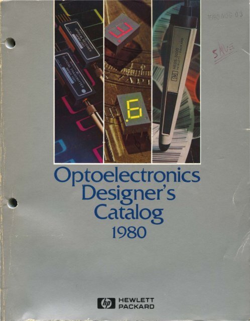
<strong>Optoelectronics</strong><br />
<strong>Designer's</strong><br />
<strong>Catalog</strong><br />
1980<br />
Flin- HEWLETT<br />
~~ PACKARD
1980 AUG 03<br />
<strong>Optoelectronics</strong><br />
<strong>Designer's</strong><br />
Intensive solid state research, the<br />
development of advanced manufacturing<br />
techniques and continued<br />
expansion has enabled Hewlett<br />
Packard to become a high volume supplier of<br />
quality, competitively priced LED displays,<br />
LED lamps, optocouplers, fiber optics, and<br />
emitters/detectors.<br />
In addition to our broad product line,<br />
Hewlett-Packard also offers the following<br />
<strong>Catalog</strong><br />
1980<br />
services: immediate delivery from<br />
any of our authorized stocking distributors,<br />
applications support,<br />
special QA testing, and a one year guarantee<br />
on all of our optoelectronic products.<br />
. This package of products and services has<br />
enabled Hewlett-Packard to become a<br />
recognized leader in the optoelectronic<br />
industry.
Hewlett-Packard is one of<br />
the world's leading designers<br />
and manufacturers<br />
of electronic, medical,<br />
analytical and computing<br />
instruments and systems.<br />
diodes. transistors. and optoelectronic products.<br />
Since its founding in Palo <strong>Al</strong>to.<br />
California, in 1939, HP has done its best to<br />
offer only products that represent significant<br />
technological advancements.<br />
To maintain its leadership in instrument and<br />
component technology. Hewlett-Packard<br />
invests heavily in new product development.<br />
Research and development expenditures<br />
traditionally average about 10 percent of sales<br />
revenue. and over 1,500 engineers and<br />
A Brief<br />
SI
These field offices are staffed by trained<br />
engineers, each of whom has the primary<br />
responsibility of providing technical assistance<br />
and data to customers. A vast<br />
communications network has been established<br />
to link each field office with the<br />
factories and with corporate offices. No<br />
matter what the product or the request, a<br />
customer can be accommodated by a single<br />
contact with the company.<br />
Hewlett-Packard is guided by a set of written<br />
objectives. One of these is "to provide<br />
products and services of the greatest possible<br />
value to our customers". Through application<br />
of advanced technology, efficient manufacturing,<br />
and imaginative marketing, it is the<br />
customer that the more than 43,000<br />
Hewlett-Packard people strive to serve. Every<br />
effort is made to anticipate the customer's<br />
needs, to provide the customer with products<br />
. that will enable more efficient operation, to<br />
offer the kind of service and reliability that will<br />
merit the customer's highest confidence, and<br />
to provide all of this at a reasonable price.<br />
To better serve its many customers' broad<br />
spectrum of technological needs, Hewlett<br />
Packard publishes several catalogs. Among<br />
these are:<br />
• Electronic Instruments and Systems for<br />
Measurement/Computation<br />
(General <strong>Catalog</strong>)<br />
• DC Power Supply <strong>Catalog</strong><br />
• Medical Instrumentation <strong>Catalog</strong><br />
• Analytical Instruments for Chemistry<br />
<strong>Catalog</strong><br />
• Coax, and WIG Measurement Accessories<br />
<strong>Catalog</strong><br />
• Diode and Transistor <strong>Catalog</strong><br />
<strong>Al</strong>l catalogs are available at no charge from<br />
your local HP sales office .<br />
Where Reputation and Quality Count<br />
When quality represents a competitive edge,<br />
or when the reputation and dependability of<br />
your products is on the line, you can count on<br />
Hewlett-Packard Optoelectronic components<br />
for excellent product consistency.<br />
decimal, and alphanumeric displays, optocouplers,<br />
fiber optics, and emitters/detectors.<br />
For a general overview of the products<br />
available, the next seven pages will include<br />
highlights of the discrete product family<br />
groups. There is complete technical data<br />
included in this designer's catalog for each of<br />
the Hewlett-Packard Optoelectronic products.<br />
The optoelectronic products available include<br />
a complete line of GaAsP and GaP discrete<br />
light emitting diodes (LED's), numeric, hexaiii
;;; . i i<br />
t<br />
~<br />
";<br />
~ i'" ~ 11<br />
"<br />
;~<br />
?<br />
- f ;<br />
~<br />
i<br />
-<br />
As the growing trend<br />
continues for microprocessor<br />
systems<br />
capable of high resolution-mechanical<br />
to<br />
electronic -interfaces,<br />
Hewlett-Packard addresses<br />
a genuine<br />
unfulfilled need with their new optical sensor.<br />
This small, self-contained optical reflective<br />
sensor combines a light source and detector<br />
with focused optics in a single package.<br />
Em itters/<br />
Detectors<br />
This unique component<br />
can detect an<br />
object as fine as a<br />
human hair as well as<br />
the precise edge of<br />
large objects such as<br />
paper or printed lines<br />
and marks. It therefore<br />
becomes ideally suited in such applications<br />
as pattern recognition, optical limit<br />
switching, tachometry, defect detection, and<br />
bar code scanning.<br />
iv
L /<br />
This optical sensor also coupled with a clean<br />
circuit design is packaged attractively in a<br />
stylized digital bar code reading wand. The<br />
wand is designed to read black and white bar<br />
codes (it will also read most colors) on a fairly<br />
flat surface. It consists of an electro-optical<br />
emitter-detector module which produces an<br />
analog Signal. followed by a current to voltage<br />
converter and then an A to D converter.<br />
The result is a computer-understandable digital<br />
electrical signal.<br />
light and spotlight configurations are ideally<br />
suited for use in optical transducers and<br />
encoders. smoke detectors. and fiber optic<br />
drivers.<br />
Hewlett-Packard PIN photodiodes are excellent<br />
light detectors with an exceptionally<br />
fast response of I ns. wide spectral response<br />
from near infrared to ultra-violet. and wide<br />
range linearity (constant efficiency over 6<br />
decades of amplitude). With dark current as<br />
low as 2S0pA at IOV. these detectors are<br />
especially well-suited for operation at low<br />
light levels. The device construction allows<br />
high speed operation at reverse voltages of<br />
5 volts. Some applications include fiber optic<br />
receivers. laser scanners. range finders. and<br />
medical diagnostic equipment. High reliability<br />
test programs are also available.<br />
In addition to the complete emitter/detector<br />
system described in both the optical scanner<br />
and digital wand. Hewlett-Packard also offers<br />
the designer the choice of discrete emitter<br />
and detector components. High radiant intensity<br />
emitters near infrared in both floodv
In 1978, Hewlett-Packard<br />
introduced its first complete<br />
fiber optic system. Fiber<br />
optics is one of the most<br />
exciting and fastest growing<br />
technologies in data transmission.<br />
With fiber optics,<br />
pulses of light travel down<br />
hair-thin fibers replacing electrical signals<br />
transmitted over copper wire. The light<br />
signals are impervious to electrical or<br />
magnetic interference .and therefore generate<br />
no electrical or magnetic noise. This<br />
makes them ideal for linking computers or<br />
control devices and their peripherals in<br />
different environments such as those found in<br />
factories, aircraft, hospitals and large power<br />
plants.<br />
A fiber optic system consists of a transmitter,<br />
a receiver, and a length of cable encasing the<br />
hair-thin glass or plastic fiber that carries<br />
optical signals. Currently, Hewlett-Packard's<br />
Fiber<br />
Optics<br />
fiber optic system is capable<br />
of receiving signals from<br />
distances up to 1000 metres.<br />
The design of cost effective<br />
fiber optic systems requires<br />
the understanding and<br />
analysis of several complex<br />
technologies - optical fibers, precision<br />
connectors, LED/laser emitters, photodetectors,<br />
circuit deSign, packaging, and optics.<br />
Hewlett-Packard's approach to the design<br />
of fiber optic hardware is systems oriented,<br />
drawing on the broad base of technologies<br />
available within our computer, instrumentation,<br />
semiconductor components, and corporate<br />
research and development activities.<br />
State-of-the-art LED, photodetector, and<br />
integrated circuit capability are at the heart of<br />
HP's fiber optic systems. Beginning on page<br />
26 of this catalog, you will find further details<br />
on Hewlett-Packard's fiber optic systems.<br />
vi
,------_.•.,----<br />
, "<br />
p<br />
which are specified<br />
t I at 400% CTR at in-<br />
OCOU P ers put currents as 10';V<br />
0<br />
Hewlett-Packard's family<br />
of optocouplers<br />
p!ovide economical,<br />
high performance solutions<br />
to problems<br />
caused by ground loops and induced common<br />
mode noise for both analog and digital<br />
applications in commercial, industrial, and<br />
military products. Hewlett-Packard's original<br />
approach towarq integrated output detectors<br />
provides performance not found in conventional<br />
phototransistor output optocouplers.<br />
With 3000 VDC isolation, the types of optocouplers<br />
available include high speed devices<br />
capable of 10M bits and high gain devices<br />
as O.5mA. In addl-<br />
tion, highly linear<br />
optocouplers are useful in analog applica-<br />
tions and a Hewlett-Packard integrated in-<br />
put optically coupled line receiver can be<br />
connected directly to twisted pair wires<br />
without additional circuitry. Most of these<br />
devices are available in dual versions, as<br />
well as in hermetic DIP packages. For military<br />
users, Hewlett-Packard's established hi-<br />
reI capability facilitates economical, hi-reI<br />
purchases.<br />
vii
Lamps<br />
Light Bar Modules are<br />
Hewlett-Packard's answer to<br />
the problem of how to effectively backlight<br />
legends. The Light Bar's large, uniformly<br />
illuminated surface provides a bright light<br />
source available in either high efficiency red,<br />
yellow, or green. The universal pinout<br />
arrangement allows connecting in parallel,<br />
series, or series/parallel configurations. Hewlett-Packard's<br />
LED Light Bar Modules are<br />
available in four sizes in a variety of<br />
arrangements including single, twin, and<br />
quad. They are X-Y stackable, and flush<br />
mounting is easy and convenient.<br />
Besides the new Light Bar Modules, Hewlett<br />
Packard LED lamps are available in a wide<br />
variety of plastic and hermetic<br />
packages to satisfy almost<br />
any application. Many styles can be mounted<br />
on a front panel using dips and all are suitable<br />
for P.c. board mounting. Hewlett-Packard<br />
military screened hermetic lamps are very<br />
popular in applications demanding highreliability.<br />
Products with wide or narrow viewing angles,<br />
and a range of brightnesses, are available in<br />
red, high efficiency red, yellow and green.<br />
Package styles include the traditional T-1-3/4,<br />
T-l, and TO-18 packages, as well as our own<br />
subminiature (stackable on 2.54mm (0.100<br />
in.) centers), rectangular, and panel mountable<br />
hermetic packages.<br />
viii
Hewlett-Packard has expanded<br />
its selection of<br />
both alphanumeric and<br />
seven-segment numeric<br />
displays to satisfy an even broader base of<br />
applications.<br />
Hewlett-Packard's completely supported<br />
alphanumeric display systems allow freedom<br />
from costly display maintenance, require very<br />
low operating power, and minimize the<br />
interaction normally required for alphanumeric<br />
displays. The display systems are TTL<br />
compatible, require a single 5V supply, and<br />
easily interface to a keyboard or microprocessor.<br />
They are ideally suited for word<br />
r,.processing equipment, instrumentation, desk<br />
:op calculators, and automatic banking<br />
Ie. terminal applications.<br />
Hewlett-Packard's yellow alphanumeric display<br />
is the answer to applications that require<br />
small size and prohibit the use of red displays.<br />
Both red and yellow alphanumeric displays<br />
feature four 5 x 7 dot matrix characters and<br />
on-board shift registers for data storage. They<br />
are contained in 16-pin DIPs which are endstackable<br />
for unlimited possibilities in alphanumeric<br />
display formatting.<br />
Available in four- and eight-character endstackable<br />
modules are HewIett-Packard's 18-<br />
segment solid state LED alphanumeric<br />
displays. Magnification of the LED by an<br />
integral lens results in<br />
a character size of<br />
3.8mm (0.15 in.) making<br />
Displays<br />
these displays ideal for use<br />
in computer peripheral products, automotive<br />
instrument panels, calculators, and electronic<br />
instruments and systems requiring low power<br />
consumption.<br />
Low cost numeric displays, packaged single<br />
or clustered, are available in character heights<br />
from .11" to .8". Low power small character<br />
displays have been designed for portable<br />
instrumentation and calculator applications.<br />
Other seven-segment display units are<br />
available in red, yellow, and green colors<br />
for use in instrumentation, point of sale<br />
terminals, and 1V indicator applications.<br />
High power, sun-light viewable, large character<br />
displays are readily adapted to outdoor<br />
terminals, gas pumps and agricultural instrumentation.<br />
For these displays, HewIett<br />
Packard has successfully integrated a gray<br />
package design with untinted segments. This<br />
results in excellent bright ambient contrast<br />
enhancement.<br />
Integrated numeric and hexadecimal displays<br />
(with on-board lC's), available in plastic and<br />
hermetic packages, solve the designer's<br />
decoding/driving problem. These displays<br />
have been designed for low cost and ease of<br />
application in a wide range of environments.<br />
ix
Hewlett-Packard has<br />
supplied specially<br />
tested high reliability<br />
optoelectronic products<br />
since 1968 for<br />
use in state-of-the-art<br />
commercial. military.<br />
and aerospace applications.<br />
To meet the<br />
requirements of high reliability. products<br />
must be designed with rugged capabilities to<br />
withstand severe levels of environmental<br />
stress and exposure without failure. We have<br />
accomplished this objective by designing a<br />
unique family of hermetic products including<br />
lamps. displays and optocouplers which have<br />
proven their merits in numerous advanced<br />
space and defense programs to the international<br />
market place. These products receive<br />
reliability screening and qualification tests in<br />
accordance with appropriate reliability programs<br />
similar to those of MIL-S-19500 and<br />
MIL-M-38510 and are supplied as either<br />
standard JAN or JANTX devices or as HP<br />
standard light reliability units which meet our<br />
in-house TXV or TXVB programs. Reliability<br />
programs are also performed to individual<br />
High<br />
Reliability<br />
customer control<br />
drawings and specifications<br />
when needed.<br />
Some of these special<br />
testing programs are<br />
very complex and<br />
may include Class S<br />
requirements for<br />
microcircuits.<br />
H P' s optoelectronic epoxy encapsulated<br />
products are designed for long life applications<br />
where non man rated or ground<br />
support requirements allow their use. As with<br />
hermetic products. the capabilities of epoxy<br />
parts can be enhanced by 100% screening and<br />
conditioning tests. Lot capabilities can be<br />
confirmed by acceptance qualification test<br />
programs.<br />
<strong>Al</strong>l testing is done by experienced Hewlett<br />
Packard employees using facilities which are<br />
either approved. or pending approval. by<br />
DESC for JAN products and by customer<br />
inspection for special programs. Environmental<br />
equipment capabilities and operating<br />
methods of the test laboratory meet MIL<br />
STD-750 or MIL-STD-883 procedures.<br />
x
This <strong>Optoelectronics</strong> <strong>Designer's</strong><br />
<strong>Catalog</strong> contains<br />
detailed, up-to-date specifications<br />
on our complete<br />
optoelectronic product line.<br />
It is divided into five major<br />
product sections: Emitters/<br />
Detectors, Fiber Optics,<br />
Optocouplers, LED Lamps, and LED Displays. A<br />
special section which includes all of the latest<br />
r', application notes in full-length version follows<br />
-, the Displays product section. Hewlett-Packard<br />
. ./ Sales and Service Offices are listed on pages<br />
475-478 and the Hewlett-Packard Components<br />
Franchised Distributors and Representatives<br />
Directory can be found on pages 472-474.<br />
How to Use This <strong>Catalog</strong><br />
Three methods are incorporated for locating<br />
components:<br />
• a Table of Contents with tabs that allow you<br />
to locate components by their general<br />
description<br />
• a Numeric Index that lists all components by<br />
part number and,<br />
• a Selection Guide for each product group<br />
giving a brief overview of the product line.<br />
About This<br />
<strong>Catalog</strong><br />
How to Order<br />
<strong>Al</strong>l Hewlett-Packard<br />
components may be ordered<br />
through any of the<br />
Sales and Service Offices<br />
listed on pages 475-478.<br />
In addition, for imme<br />
diate delivery of Hewlett<br />
Packard optoelectronic components, contact<br />
any of the world-wide stocking distributors<br />
and representatives listed on pages 472-474.<br />
Warranty<br />
HP's Components are warranted against defects<br />
in material and workmanship for a period<br />
of one year from the date of shipment.<br />
HP will repair or, at its option, replace Components<br />
that prove to be defective in material<br />
or workmanship under proper use during<br />
the warranty period. This warranty extends<br />
only to HP customers.<br />
No other warranties are expressed or implied,<br />
including but not limited to, the implied<br />
warranties or merchantability and fitness for<br />
a particular purpose. HP is not liable for<br />
consequential damages.<br />
xi
Table of Contents<br />
xii
Numeric Index ...................................................... xiv<br />
Emitters/Detectors<br />
Emitter and Detector Systems: Features. Advantages. Benefits .................... 2<br />
Emitters and Detectors: Features. Advantages. Benefits .......................... 3<br />
Optical Scan:1er ............................................................. 4<br />
Digital Bar Code Wand ...................................................... 10<br />
Emitters and Detectors ...................................................... 16<br />
fiber Optics<br />
Features. Advantages. Benefits ............................................... 26<br />
Transmitters ................................................................ 28<br />
Receiver ................................................................... 36<br />
Cables ..................................................................... 40<br />
Optocouplers<br />
Selection Guide ............................................................ 44<br />
High Speed Optocouplers ................................................... 46<br />
High Gain Optocouplers .................................................... 72<br />
AC/DC to Logic Interface Optocoupler ....................................... 84<br />
Hermetic Optocoupler ...................................................... 90<br />
Solid State Lamps<br />
Selection Guide ........................................................... 106<br />
Red. High Efficiency Red. Yellow and Green Lamps ............................. 113<br />
Integrated Lamps .......................................................... 159<br />
Hermetically Sealed Lamps ................................................. 165<br />
Panel Mounting Kit ......................................................... 171<br />
Solid State Displays<br />
Selection Guide ........................................................... 174<br />
Red. High Efficiency Red. Yellow and Green Seven Segment Displays ........... 180<br />
Red Seven Segment Displays ............................................... 208<br />
Integrated Displays ........................................................ 232<br />
Hermetically Sealed Integrated Displays ...................................... 241<br />
<strong>Al</strong>phanumeric Displays ..................................................... 253<br />
High Reliability<br />
Introduction .............................................................. 306<br />
Selection Guide ........................................................... 308<br />
Appllcadons Information<br />
Application Bulletins. Notes and Manual Listing ............................... 312<br />
Abstracts ................................................................. 313<br />
Appendix<br />
HP Components Franchised Distributor and Representative Directory ........... 472<br />
Hewlett-Packard Sales and Service Offices ................................... 475<br />
Profile and Inquiry Card<br />
xiii
-"""<br />
HCPL-2502 ................ . . . .. 46<br />
HCPL-2530 . . . . . . . . . . . . . . . . . . . .. 50<br />
HCPL-2531 ...................... 50<br />
HCPL-2601 ...................... 58<br />
HCPL-2602 ...............•..... 62<br />
HCPL-2630 ...................... 68<br />
HCPL-2730 .......•.............. 76<br />
HCPL-2731 ...................... 76<br />
HCPL-3700 ...................... 84<br />
HDSP-2000 .................... 253<br />
HDSP-2001 ..................... 257<br />
HDSP-2010 ...................... 261<br />
HDSP-2416 ..................... 265<br />
HDSP-2424<br />
HDSP-2432<br />
HDSP-2440<br />
265<br />
HDSP-2470 .................... 265<br />
HDSP-2471 ..................... 265<br />
HDSP-2472 265<br />
HDSP-3400 .................... 204<br />
<strong>Al</strong>phanumeric<br />
Index<br />
265<br />
265<br />
HDSP-3401 ..................... 204<br />
HDSP-3403<br />
204<br />
HDSP-3405<br />
204<br />
HDSP-3406<br />
204<br />
HDSP-3530 ..................... 190<br />
HDSP-3531 ...................... 190<br />
HDSP-3533 ..................... 190<br />
HDSP-3536 .............•....... 190<br />
HDSP-3730 ..................... 190<br />
HDSP-3731 ...................... 190<br />
HDSP-3733 ..................... 190<br />
HDSP-3736 ..................... 190<br />
HDSP-4030 ..................... 190<br />
HDSP-4031 ...................... 190<br />
HDSP-4033 ..................... 190<br />
HDSP-4036 ..................... 190<br />
HDSP-4130 ...................... 190<br />
HDSP-4131 ...................... 190\<br />
HDSP-4133 ..............•.....•. 190<br />
HDSP-4136 ...................... 190<br />
HDSP-6300 .................... 277<br />
HDSP-6504 .................... 282<br />
HDSP-6505 ••••••••••••••••<br />
HDSP-6508 ••••••••••••••<br />
HDSP-6509 ••••••<br />
0 ••• 282<br />
0.0 •• 0 282<br />
0 ••••• 0 ••••••• 282<br />
* HDSP-8716 ..................... 288<br />
* HDSP-8724 ..................... 288<br />
* HDSP-8732 ..................... 288<br />
*HDSP-8740 ..................... 288<br />
HEDS-I000 ........................ 4<br />
* New Product.<br />
xiv
*HEDS-3000 ...................... 10<br />
HEMT-3300 ...................... 16<br />
HEMT-6000 ...................... 18<br />
HFBR-0010 ....................... 27<br />
HFBR-l00l ....................... 28<br />
* HFBR-l002 ....................... 32<br />
HFBR-2001 ....................... 36<br />
* HFBR-3000 ...................... 40<br />
HLMP-0300 ..................... 127<br />
HLMP-0301 ..................... 127<br />
HLMP-0400 ..................... 127<br />
HLMP-0401 ..................... 127<br />
HLMP-0500 ..................... 127<br />
HLMP-0501 127<br />
HLMP-1300 ..................... 123<br />
HLMP-1301 ...................... 123<br />
HLMP-1302 ..................... 123<br />
HLMP-1400 ..................... 123<br />
HLMP-1401 ...................... 123<br />
HLMP-1402 123<br />
HLMP-1500 ..................... 123<br />
HLMP-1501 ...................... 123<br />
HLMP-1502 ..................... 123<br />
HLMP-2300 ..................... 135<br />
HLMP-2350 ..................... 135<br />
HLMP-2400 ..................... 135<br />
HLMP-2450 ..................... 135<br />
HLMP-2500 ..................... 135<br />
HLMP-2550 ..................... 135<br />
* HLMP-2600 ..................... 139<br />
* HLMP-2620 ..................... 139<br />
* HLMP-2635 ..................... 139<br />
* HLMP-2655 ..................... 139<br />
* HLMP-2670 ..................... 139<br />
* HLMP-2685 ..................... 139<br />
* HLMP-2700 ..................... 139<br />
* HLMP-2720 ..................... 139<br />
* HLMP-2735 ..................... 139<br />
* HLMP-2755 ..................... 139<br />
*HLMP-2770 ..................... 139<br />
*HLMP-2785 ..................... 139<br />
*HLMP-2800 ..................... 139<br />
*HLMP-2820 ..................... 139<br />
*HLMP-2835 ..................... 139<br />
* HLMP-2855 ..................... 139<br />
* HLMP-2870 ..................... 139<br />
* HLMP-2885 ..................... 139<br />
* HLMP-3105 ..................... 157<br />
*HLMP-3112 ...................... 157<br />
* HLMP-3600 ..................... 155<br />
*'HLMP-3650 ..................... 155<br />
* HLMP-3680 ..................... 155<br />
HLMP-6203 ..................... 153<br />
HLMP-6204 ..................... 153<br />
HLMP-6205 ..................... 153<br />
HLMP-6600 ..................... 163<br />
HLMP-6620 ..................... 163<br />
HPBK-l000 ...................... 314<br />
jANTX1N5765 ................... 165<br />
jANTX1N6092 ................... 165<br />
jANTX1N6093 ........•.......... 165<br />
jANTX1N6094 ................... 165<br />
jAN1N5765 ..................... 165<br />
jAN1N6092 ..................... 165<br />
jAN1N6093 ..................... 165<br />
jAN1N6094 ..................... 165<br />
MI9500/519-01 ............•..... 165<br />
MI9500/519-02 ................. 165<br />
MI9500/520-01 ................. 165<br />
MI9500/520-02 ................. 165<br />
MI9500/521-01 .................. 165<br />
MI9500/521-02 ................. 165<br />
lN5765 ......................... 165<br />
lN6092 ......................•.. 165<br />
lN6093 ......................••. 165<br />
lN6094 ......................... 165<br />
*4N55 .........................•.. 98<br />
* 4N55-TXV ...................•.•.. 98<br />
*4N55-TXVB ...................... 98<br />
* New Product.<br />
xv
5082-4100 ....................... 131<br />
5082-4101 ....................... 131<br />
5082-4150 ....................... 131<br />
5082-4160 ....................... 131<br />
5082-4190 ....................... 131<br />
5082-4203<br />
5082-4204<br />
5082-4205<br />
5082-4207<br />
5082-4220<br />
...................... 20<br />
20<br />
...................... 20<br />
...................... 20<br />
...................... 20<br />
5082-4403 ..................... 147<br />
5082-4415 ...................... 147<br />
5082-4440<br />
147<br />
5082-4444<br />
147<br />
5082-4468<br />
159<br />
5082-4480<br />
5082-4483<br />
5082-4484<br />
5082-4486<br />
5082-4487<br />
5082-4488<br />
149<br />
149<br />
145<br />
149<br />
149<br />
149<br />
5082-4494 ..................... 145<br />
5082-4550 ...................... 113<br />
5082-4555 ...................... 113<br />
5082-4557 ...................... 113<br />
5082-4558 .........•............ 113<br />
5082-4587 ..................... 165<br />
5082-4590 ...................... 11 7<br />
5082-4592 ...................... 117<br />
5082-4595 ...................... 11 7<br />
5082-4597 ...................... 11 7<br />
5082-4650 ...................... 113<br />
5082-4655 ...................... 113<br />
5082-4657 ...................... 113<br />
5082-4658 ...................... 113<br />
5082-4687 ..................... 165<br />
5082-4690 ...................... 11 7<br />
5082-4693 ...................... 117<br />
5082-4694 ...................... 11 7<br />
5082-4695 ...................... 117<br />
5082-4707 ...................... 171<br />
5082-4732 ...................... 161<br />
5082-4787 ..................... 165<br />
5082-4790 ...................... 11 7<br />
5082-4791 ....................... 117<br />
5082-4850<br />
145<br />
5082-4855<br />
145<br />
5082-4860<br />
159<br />
5082-4880<br />
147<br />
5082-4881 ...................... 147<br />
5082-4882<br />
5082-4883<br />
5082-4884<br />
5082-4885<br />
5082-4886<br />
5082-4887<br />
5082-4888<br />
147<br />
147<br />
147<br />
147<br />
147<br />
147<br />
147<br />
5082-4950 ...................... 113<br />
5082-4955 ...................... 113<br />
5082-4957 ...................... 113<br />
5082-4958 ...................... 113<br />
5082-4987 ..................... 165<br />
5082-4990 ...................... 11 7<br />
5082-4992 ...................... 117<br />
5082-4995 ...................... 117<br />
5082-4997 ...................... 117<br />
5082-7010 ...................... 241<br />
5082-7011 ...................... 241<br />
5082-7100 ...................... 300<br />
5082-7101 ...................... 300<br />
5082-7102 ...................... 300<br />
5082-7240 ..................... 224<br />
5082-7241 ...................... 224<br />
5082-7265 ..................... 228<br />
5082-7275 ..................... 228<br />
5082-7285 ..................... 228<br />
5082-7295 ..................... 228<br />
5082-7300 ..................... 232<br />
* New Product.<br />
xvi
-<br />
5082-7302 ..................... 232<br />
5082-7304 ..................... 232<br />
5082-7340 ..................... 232<br />
5082-7356 ..................... 236<br />
5082-7257 ..................... 236<br />
5082-7358 ..................... 236<br />
5082-7359 ..................... 236<br />
5082-7391 ...................... 247<br />
5082-7392 ..................... 247<br />
5082-7393 ..................... 247<br />
5082-7395 ..................... 247<br />
5082-7402 ..................... 208<br />
5082-7403 ..................... 208<br />
5082-7404 ..................... 208<br />
5082-7405 ..................... 208<br />
5082-7412 ...................... 208<br />
5082-7413 ...................... 208<br />
5082-7414 ...................... 208<br />
5082-7415 ...................... 208<br />
5082-7432 ..................... 212<br />
5082-7433 •••• I ••• I •••• II ••• I •• 212<br />
5082-7440 • ••••• II. I ••• II •••••• 216<br />
5082-7441 ••• 1 •• II. II I. I ••••• II. 216<br />
5082-7442 • II "' II ••• II II •••• II. 216<br />
5082-7444 ••• I. I. II II. II II ••••• 216<br />
5082-7445 •••• II ••• II •• I., ••• II 216<br />
5082-7446 •••• I •••••••• 11 •• 1 ••• 216<br />
5082-7447 • I. I. 1 •••• 1. II ••••••• 216<br />
5082-7448 .1. II II •• I •• "' II ••••• 216<br />
5082-7449 ••••• II •• II •• I ••••• I. 216<br />
5082-7610 I •••• II ••• II •• I ••••••• 180<br />
5082-7611 II ••••• II. II •• 11.1.1 •• 180<br />
5082-7613 •• I. 11.1 ••••• I •••••••• 180<br />
5082-7616 •• I. II II ••••• II I ••• I., 180<br />
5082-7620 I.' II •••• II. II •••• II. 180<br />
5082-7621 •••••••••• II ••• II ••••• 180<br />
5082-7623 •••• II ••• II •• II •••••• 180<br />
5082-7626 •••••• II •• II II. II •••• 180<br />
5082-7630 • II II 1 ••••••• 1 II ••••• 180<br />
5082-7631 ...................... 180<br />
5082-7633 ..................... 180<br />
5082-7636<br />
180<br />
5082-7650<br />
185<br />
5082-7651 ...................... 185<br />
5082-7652 ..................... 185<br />
5082-7653<br />
185<br />
5082-7656<br />
185<br />
5082-7660<br />
185<br />
5082-7661 ...................... 185<br />
5082-7662<br />
5082-7663<br />
5082-7666<br />
185<br />
185<br />
185<br />
5082-7670<br />
185<br />
5082-7671 ...................... 185<br />
5082-7672<br />
5082-7673<br />
5082-7676<br />
185<br />
185<br />
185<br />
5082-7730<br />
196<br />
5082-7731 ...................... 196<br />
5082-7732 ..................... 196<br />
5082-7736 ..................... 196<br />
5082-7740 196<br />
5082-7750 ..................... 200<br />
5082-7751 ...................... 200<br />
5082-7752 ......... ;........... 200<br />
5082-7756 ..................... 200<br />
5082-7760 ......•.............. 200<br />
6N134 ........................... 90<br />
6N134-TXV ....................... 90<br />
6N134-TXVB ...................... 90<br />
6N135 '" ......................... 46<br />
6N136 ........................... 46<br />
6N137<br />
6N138<br />
6N139<br />
........................... 54<br />
........................... 72<br />
72<br />
*6N140 ........................... 94<br />
* 6N140-TXV ....................... 94<br />
* 6N140-TXVB .....••............... 94<br />
* New Product.<br />
xvii<br />
~:-..,...':.~~~ ......"'.---.--........--------------------------
: \'<br />
,'~ " ,<br />
",: >~,'<br />
", :;,~<br />
'.'<br />
" ,,'
, " ~' :<br />
'::,\<br />
~", ,"
Emitter/Detector Systems<br />
• Features • Advantages • Benefits<br />
HEDS-1000 HIGH RESOLUTION OPTICAL REFLECTIVE SENSOR<br />
Focused optics<br />
Visible light source<br />
Photo IC detector<br />
Standard TO-5 package<br />
Sealed package<br />
Detector IC operates from<br />
single ended 3.5V to 20V<br />
power supply<br />
Fully integrated, assembled<br />
and tested<br />
Performance fully specified<br />
and guaranteed<br />
Gives higher resolution<br />
Can detect most colors<br />
A. Faster response time<br />
B. Speed, linearity, and<br />
gain options available<br />
Mounting hardware<br />
readily available<br />
Moisture resistant<br />
Compatible with all IC<br />
technologies<br />
No precision alignment<br />
required<br />
System design simplified<br />
Less error<br />
No precision alignment of<br />
discrete components<br />
Not limited to black & white<br />
patterns and objects<br />
A. Can detect more transitions<br />
in less time<br />
B. Simplified interface<br />
electronics<br />
Easy to mount and use<br />
Reliable operation in indoor/<br />
outdoor environments<br />
Easy to use<br />
Easy to use<br />
Faster design-in<br />
Assured performance<br />
HEDS-3000 DIGITAL BAR CODE WAND<br />
Digital output<br />
Low digitizing error<br />
Push-to-read switch<br />
Guaranteed performance<br />
Single supply operation<br />
Lightweight stylized<br />
plastic case<br />
Custom options<br />
available<br />
No analog signal<br />
conditioning circuitry<br />
needed<br />
High percentage<br />
Good reads<br />
Conserves power<br />
No strobing circuitry<br />
required<br />
System design simplified<br />
Compatible with standard<br />
digital systems<br />
Minimizes operator fatigue<br />
Styling to match<br />
customer's products<br />
Microprocessor compatible<br />
Increased throughput<br />
Longer battery life<br />
in portable systems<br />
Easy to use<br />
Easy to use<br />
Increased throughput<br />
OEM product image<br />
enhanced<br />
2
~<br />
Emitters<br />
• Features<br />
Near IR emission<br />
Functions with most<br />
silicon phototransistors<br />
and photodiodes<br />
Plastic Package<br />
HEMT 3300 uses isotropic<br />
LED chip<br />
HEMT 6000 uses surface<br />
emitter LED chip<br />
HEMT 6000 has offset<br />
wirebond<br />
• Advantages<br />
Visible<br />
Easy to use<br />
Low cost<br />
Provides floodlight type<br />
beam<br />
Provides bright spot<br />
of light<br />
Active area of the chip<br />
is not masked or<br />
shadowed<br />
• Benefits<br />
Facilitates alignment<br />
Cost effective implementation<br />
Cost effective implementation<br />
Well suited for applications<br />
that require a large area to<br />
be irradiated<br />
Facilitates focusing light on<br />
active area of photodetector<br />
Facilitates use with fiber<br />
optics<br />
• Features<br />
Offset wirebond<br />
.~/ <strong>Al</strong>l HP PIN photodiodes<br />
have anti~reflective coating<br />
Wide spectral response<br />
(ultraviolet through IR)<br />
Low junction capacitance<br />
ULTRA Linear<br />
Detectors<br />
(PIN Photodiodes)<br />
• Advantages<br />
Can be used with fiber<br />
optiCS<br />
Converts more incident<br />
radiation (light) into<br />
photocurrent<br />
A single device can cover<br />
the light spectrum plus<br />
UV and IR<br />
Wide bandwidth<br />
Permits operation over<br />
10 decades<br />
• Benefits<br />
Fiber can be placed directly<br />
over active area<br />
High Responsivity<br />
Works with a variety of<br />
sources<br />
Can detect high speed pulses<br />
Eliminates the need for<br />
equalization<br />
3
HEWLETT<br />
PACKARD<br />
HIGH 'RESOLUTION<br />
,OPTICAL', REFLECTIVE<br />
, '." . "'SENSOR<br />
- : ,,-:,<br />
-,TERS AND (INCHES),<br />
2. ALL UNTOlERANCeD DIMeNSIONS AftE fOR REFERENCE DNL Y,<br />
3. THE REFERENCE PLANE IS THE TOP SURFACe Of THE PACKAGE.<br />
4. NICKEL CAN AND GOlO PLATED LEADS.<br />
5. $.P. SEATING PLANE,<br />
6. THE LEAO DIAMETER IS 0._ ID.Ol81n.1 TYP.<br />
4
Electrical Operation<br />
The detector section of the sensor can be connected as a<br />
single photodiode, or as a photodiode transistor amplifier.<br />
When photodiode operation is desired, it is recommended<br />
that the substrate diodes be defeated by connecting the<br />
collector of the transistor to the positive potential of the<br />
power supply and shorting the base-emitter junction of<br />
the transistor. Figure 15 shows photocurrent being<br />
supplied from the anode of the photodiode to an inverting<br />
input of the operational amplifier. The circuit is<br />
recommended to improve the reflected photocurrent to<br />
stray photocurrent ratio by keeping the substrate diodes<br />
from acting as photodiodes.<br />
The cathode of the 700nm emitter is physically and<br />
electrically connected to the case-substrate of the device.<br />
Applications that require modulation or switching of the<br />
LED should be designed to have the cathode connected to<br />
the electrical ground of the system. This insures minimum<br />
capacitive coupling of the switching transients through<br />
the substrate diodes to the detector amplifier section.<br />
The HEDS-1000 detector also includes an NPN transistor<br />
which can be used to increase the output current of the<br />
sensor. A current feedback amplifier as shown in Figure 6<br />
provides moderate current gain and bias point stability.<br />
SCHEMATIC DIAGRAM<br />
CONNECTION DIAGRAM<br />
VD<br />
Vc<br />
REFLECTOR<br />
REFERENCE I \. t<br />
PLANE t !!..- V\ +<br />
) 1 ,<br />
~<br />
CAT~ 1 ____<br />
---'<br />
SUBSTRATE,CASE<br />
OS-SUBSTRATE DIODES<br />
VB<br />
VE<br />
PIN FUNCTION "--c.<br />
1 TRANSISTOR COLUCTOR<br />
2 TIWmSTOR 8ASE,'PjiOToptOOt; ANooe<br />
3 'PHOTODIOOt; CATJiOl>E' ~ .~<br />
4 .'t.I!l>'CAttlOl>E, SUBSl'RATE;C<strong>Al</strong>!Ii ..:c<br />
5' 'Ne:: .' 'r' .' .<br />
/I Mm~ODe, 2 ~:.i<br />
7 . NIl '." . .·2':·"f'~.-:<br />
II :'mAI'ISISTOR £MITTER ..;,,:;-.> ".<br />
TOP VIEW<br />
f<br />
~ -<br />
Absolute Maximum Ratings at TA=25°C<br />
Parameter Symbol Mfn. Max,<br />
......<br />
. ","1$'; FIg, 2 ... Notes<br />
Storage Temperature TS -40 +75<br />
, ·c·;<br />
.. '<br />
Operating Temperature TA -.20 '. +70 "C-<br />
,.; ..•.. ';: '2..::····<br />
Lead Soldering Temperature :. ·260.',,:<br />
I."<br />
'·~?t;~:· t·,,::·,; '; IX,.~,l .<br />
1 ,6mm from Seating Plane .....• .. fOr105eo.; •• ,. '.,> .. ::<br />
Average LEO Forward Current IF ..... "'. ..... liO<br />
,<br />
System Electrical/Optical Characteristics at TA =25°C<br />
Parameter Symbol Min. Typ. Max. Unite Conditions Fig. Note<br />
375 TA=-20'C<br />
Total Photocurrent (lPR+lps) Ip 100 140 250 nA TA=25'C IF=35mA, VD=Vc=5V 2.3 4<br />
Reflected Photocurrent OPRl to<br />
IPR<br />
50 TA=70'C 15<br />
Internal Stray Photocurrent (Ips) iPS 4 6.5 Ip=35mA, Vc=Vo=5V 3<br />
Transistor DC Static Current h 50 TA=-20'C<br />
Fe Vce=5V, Ic=10!,A 4,5<br />
Transfer Ratio 100 200 TA-25'C<br />
Slew Rate .06 VII's RL=100K IpK=50mA 6<br />
RF= 10M tON=100!,s, Rate = 1 kHz<br />
Image Diameter d .17 mm If=35mA,Q=4.27mm 10.168In.) 8.10 8,9<br />
Maximum Signal Point Q 4.02 4.27 4.52 mm Measured from Reference Plane 9<br />
50% Modulation Transfer<br />
Function MTF 2.5 loprlmrr IF"'35mA, Q =4.27mm 10,11 5,7<br />
Depth of Focus<br />
Effective Numerical Aperature NA .3<br />
.lQ<br />
FWHM 1.2 mm 50% of Ip atQ""4.27mm 9 5<br />
Image Location D .51 mm Diameter Reference to Centerline 6<br />
Q=4.27mm<br />
Thermal Resistance 0JC 85 'C/W<br />
Detector Electrical/Optical Characteristics at TA =25°C<br />
Parameter Symbol Min. Typ. Max. Units Conditions Fig. Note<br />
Dark Current Ipo 5 120 pA TA=25'C I IF=Q, Vo=SV;<br />
10 nA TA=70'CI Reflection=O%<br />
CapaCitance Co 45 pF Vo=OV, Ip=O, 1=1 MHz<br />
Flux Responslvity Rd> .22 ..h... ,\.=700nm, Vo=5V 12<br />
W<br />
Detector Area . Ao ,160 mm2 Square. with Length=Amm/Side<br />
Emitter Electrical/Optical Characteristics at TA=25°C<br />
Parameter Symbol Min. Typ. Max. Units Conditions Fig. Note<br />
Forward Voltage VF 1.6 1,8 V IF=35rnA 13<br />
Reverse Breakdown Voltage eVR 5 V IR=1001"A<br />
Radiant Flux if>E 5 9,0 !'W IF=35mA, ,\.=700nm 14<br />
-<br />
Peak Wavelength '\'p 680 700 720 nm IF=35mA 14<br />
Thermal Resistance 0JC 150 "CIW<br />
. Temperature Coefficient of VF tNF/.:.r ·1.2 mV/'C IF=35mA<br />
6
~<br />
Transistor Electrical Characteristics at TA=25°C<br />
Parameter Symbol Min. Typ. Uax. Units Conditions Fi(j. Nola<br />
Collector-Emitter Leakage ICEO 1 pfA, VCE"'5V<br />
Base-Emitter VOltage VeE .6 V 1c=10pA •. ts=70nA<br />
Collector-Emitter Saturation<br />
Voltage VceISAT) .4 V 's=1~. Ie=10PA<br />
Collector·Base CapaCitance CCB .3 pF f=1MHz, Vce=5V<br />
~$e-Emitter Capacitance CBe .4 pF f='lMHz, VBE=OV<br />
.Thermal Resistance eJC 200 'C/W<br />
NOTES:<br />
1. 300l's pulse width, 1 kHz pulse rate.<br />
2. Derate Maximum Average Current linearly from 65· C by 6mA/· C.<br />
3. Without heat sinking from TA = 65·C, derate Maximum Average Power linearly by 12mW/·C.<br />
4. Measured from a reflector coated with a 99% reflective white paint (Kodak 6080) positioned 4.27mm (0.168 in.) from the reference plane.<br />
5. Peak-to-Peak response to black and white bar patterns.<br />
6. Center of maximum signal point image lies within a circle of diameter D relative to the center line of the package. A second emitter<br />
image (through the detector lens) is also visible. This image does not affect normal operation.<br />
7. This measurement is made with the lens cusp parallel to the black-white transition.<br />
8. Image size is defined as the distance for the 10%-90% response as the sensor moves over an abrupt black-white edge.<br />
9. (+) Indicates an increase in the distance from the reflector to the reference plane.<br />
10. <strong>Al</strong>l voltages referenced to Pin 4.<br />
11. CAUTION: The thermal constraints of the acrylic lens will not permit the use of conventional wave soldering procedures. Thetypical<br />
preheat and post cleaning temperatures and dwell times can subject the lens to thermal stresses beyond the absolute maximum<br />
ratings and can cause it to defocus.<br />
2.01-~~+l+ttit-++tttHtt--t.,.H+ttitl-~-++Hftil<br />
1.81-·-+~+l+ttit-++tttHtt--t--H+ttitl-~-++Hftil<br />
1.61--I-I-++++H+--I-I-++++H1--I-I-+++H+1--I-I-+++++il'<br />
1.4 \ I \ \1r-t-f1"rtf+H1l<br />
~~+H~-\~~l~~~~~- £ ~~~,~-~~~~<br />
1.2 iii ~ 1----'* *<br />
r-IrH~~+I\~~~~,~~~--+\~~<br />
1.0 L...-.1.-L..J....U..'-'-':':---'---"-'-Li.LJ..£H L..--'---IL..l...W..I,-,-,,---,-'...JL.J...J..U.UI<br />
1 10 100 1000 10.000<br />
tp - PULSE OURATION IllS)<br />
Figure 1. Maximum Tolerable Peak Current vs; Pulse Duration<br />
IF - DC FORWARD CURRENT (mA)<br />
60 70 80<br />
Figure 2. Relative Total Photocurrent vs. LED DC<br />
Forward Currem<br />
HP01n<br />
;
U<br />
~'ln<br />
",N<br />
'" "<br />
3.0<br />
~~<br />
0:'" 2.0<br />
0: c<br />
::>8<br />
u~<br />
0"<br />
0: "<br />
"'- ;:t-<br />
0:'"<br />
00<br />
u.w 1.0<br />
g~<br />
I'"<br />
~~<br />
.cO<br />
~<br />
!<br />
1 :.'.<br />
~. . 1O'C<br />
1ik<br />
; II<br />
i i: :m'C<br />
fo" ~ ~ II<br />
fo" .....,. ~ I<br />
fo" .......<br />
.......•<br />
i<br />
. ..- -2O"C<br />
100 1000 10,000<br />
18 - BASE CURRENT (nA)<br />
;;<br />
-'I 40<br />
t-<br />
fi'i<br />
0:<br />
0:<br />
::><br />
u<br />
0:<br />
g<br />
u<br />
;<br />
30<br />
20<br />
"...-- 0<br />
u<br />
1<br />
J; 10<br />
50<br />
I. - BASE CURRENT (n<strong>Al</strong><br />
I-TEMP • 25" C<br />
,EP'l<br />
~<br />
-" ...... ~<br />
-~ -i-""'" ,'$>"p<br />
-i-""'" ,~<br />
-i-""<br />
~<br />
~<br />
-f-<br />
6I!!!e-<br />
...... .....,. roo-<br />
-.....,.<br />
~<br />
.....,.,....<br />
.-<br />
~1.<br />
20nA<br />
J<br />
8 10 12 14 16 18 20<br />
VeE - COLLECTOR-TO-EMITTER VOLTAGE (V)<br />
Figure 4. Normalized Transistor DC Forward Current Gain vs.<br />
Base Current at Temperature<br />
Figure 5. Common Emitter Collector Characteristics<br />
IFPK =5OmA<br />
tp-l00IlS, RATE = 1KHz<br />
REFERENCE f<br />
Vee" 5V -~--,<br />
REFLECTOR<br />
\ ! 3<br />
==<br />
PLANEr ~ tl<br />
+------.--Vo<br />
-----,<br />
I<br />
I<br />
*".<br />
_____ J I<br />
R,<br />
r<br />
DETECTOR IMAGE<br />
THROUGH EMITTER<br />
LENS<br />
MAXIMUM<br />
SIGNAL POINT<br />
\ EMITTER IMAGE<br />
l THROUGH DETECTOR<br />
LENS<br />
Figure 6. Slew Rate Measurement Circuit<br />
Figure 7. I mage Location<br />
0.4<br />
0.3<br />
I<br />
w<br />
N<br />
;;;<br />
w 0.2<br />
~<br />
~<br />
O. 1<br />
\<br />
\<br />
S£~ NOT~S; 7 .~.9<br />
"- ......... ro-<br />
.<br />
o<br />
-O.B -0.6 -0.4 -0.2 0.2 0.4 0.6 O.B<br />
110<br />
0<br />
0<br />
0<br />
0<br />
0<br />
0<br />
0<br />
0<br />
I<br />
I<br />
i<br />
II<br />
r<br />
1\<br />
\<br />
~£ ..<br />
'i -<br />
"\.<br />
iI£ - DISTANCE FROM MAXIMUM SIGNAL (mm)<br />
12 - REFLECTOR DISTANCE (mm)<br />
Figure S. Image Size vs. Maximum Signal Point<br />
Figure 9. Reflector Distance vs. % Reflected Photocurrent<br />
8
110<br />
lOa<br />
"-<br />
;!,.<br />
90<br />
z<br />
0<br />
80<br />
§ 70<br />
:::><br />
0 ":;<br />
60<br />
w 50<br />
":::> .... 40<br />
i 30<br />
:;<br />
20<br />
..<br />
10<br />
m<br />
L<br />
1\ J<br />
L<br />
\. I"'"<br />
.'<br />
'\: .... ¢<br />
."<br />
.. 1'"<br />
I<br />
. ,<br />
."<br />
.:"'10 '.<br />
... r--.<br />
.:. I' I· ~<br />
.:Id - EDGE DISTANCE (mm)<br />
SPATIAL FREQUENCY (LINE PAIR/mm)<br />
Figure 10. Step Edge Response<br />
Figure 11. Modulation Transfer Function<br />
100<br />
90<br />
80<br />
70<br />
w<br />
U)<br />
z 60<br />
0<br />
~ 50<br />
..<br />
II:<br />
40<br />
30<br />
.....<br />
J~<br />
I ~<br />
/ ~<br />
~,<br />
~<br />
~<br />
~ C<br />
26"C"<br />
20<br />
I<br />
10<br />
I<br />
600 700 800 900 1000<br />
A - WAVELENGTH (nm)<br />
VF - FORWARD VOLTAGE (V)<br />
Figure 12. Detector Spectral Response<br />
Figure 13. LED Forward Current vs. Forward Voltage<br />
Characteristics<br />
1.2<br />
1.0<br />
0.8<br />
0.6<br />
0.4<br />
I\O'C<br />
I<br />
,<br />
26"C<br />
I<br />
I<br />
II<br />
I<br />
i/I.<br />
fl I<br />
70'C<br />
O. 2<br />
I ~\.<br />
~V .~[\.<br />
e. ~ ~<br />
~o 660 680 700 720 740 760<br />
x. - WAVELENGTH (nm)<br />
REFLECTOR<br />
REFERENCE ;I \ +<br />
PLANEr t<br />
ANODE<br />
CATHODE 4<br />
SUBSTRATE. CASE<br />
~I<br />
~<br />
rp<br />
---4- -<br />
Vee<br />
--,<br />
I<br />
~s<br />
I<br />
_..J<br />
8<br />
VOUT<br />
Figure 14. Relative Radiant Flux vs. Wavelength<br />
Figure 15. Photodiode Interconnection<br />
9
',' "., ,DIGITAL<br />
BAR CODE WAND<br />
Features<br />
• 0.3 mm RESOLUTION<br />
Enhances the Readability of dot matrix printed<br />
bar codes<br />
• DIGITAL OUTPUT<br />
Open Collector Output Compatible<br />
with TTL and CMOS<br />
• PUSH-TO-READ SWITCH<br />
Wand Consumes Power Only When Switch is<br />
Depressed<br />
• SINGLE SUPPLY OPERATION<br />
• STYLIZED CASE<br />
• DURABLE LOW FRICTION TIP<br />
• SOLID STATE RELIABILITY<br />
Uses LED and IC Technology<br />
Description<br />
The HEDS-3000 Digital Bar Code Wand is a hand held<br />
scanner with integral push-to-read switch. It is designed<br />
to read all common bar code formats that have the<br />
narrowest bars printed with a nominal width of 0.3 mm<br />
(0.012 in.). The wand contains an optical sensor with a 700<br />
nm visible light source, photo IC detector, and precision<br />
aspheric optics. Internal signal conditioning circuitry<br />
converts the optical information into a logic level pulse<br />
width representation of the bars and spaces.<br />
The HEDS-3000 comes equipped with a push-to-read<br />
switch which is used to activate the electronics, and strain<br />
relieved 104 cm (41 in.) cord with nine-pin subminiature<br />
D-style connector.<br />
wand Dimensions<br />
Applications<br />
The Digital Bar Code Wand is an effective alternative to<br />
the keyboard when used to collect information in selfcontained<br />
blocks. Bar code scanning is faster than key<br />
entry and also more accurate since most codes have<br />
check-sums built-in to prevent incorrect reads from being<br />
entered.<br />
Applications include remote data collection, ticket<br />
identification systems, security checkpoint verification,<br />
file folder tracking, inventory control, identifying assemblies<br />
in service, repair, and manufacturing environments,<br />
and programming appliances, intelligent instruments and<br />
personal computers.<br />
" 23(0.91-,<br />
------. jl~ --.,--~;-- '050 141.0) -----t~ I<br />
r---------~I' ~ -t:,U.Iol.I,l:':CJO]<br />
. m;:E;lL OIMENSt()N$ IN Ml~LlMETRES AND IINCHES). ,0 (08) J<br />
2, WEIGHT, ~ .. 4ti,S. 11.5 ... l. Shit>!>lng 171g 15,5 ...).<br />
10
Recommended Operating<br />
Conditions<br />
Absolute Maximum Ratings<br />
Electrical Operation<br />
The HEDS-3000 consists of a precision optical sensor, an<br />
analog r amplifier, a digitizing circuit, and an output<br />
transistor. These elements provide a TTL compatible<br />
output from a single voltage supply range of 3.6V to 5.75V.<br />
A non-reflecting black bar results in a logic high (11 level,<br />
while a reflecting white space will cause a logic low (01 at<br />
the Va connection (pin 21. The output of the HEDS-3000 is<br />
an open collector transistor.<br />
A push-to-read switch is used to energize the 700 nm LED<br />
emitter and electronic circuitry. When the switch is<br />
initially depressed, its contact bounce may cause a series<br />
of random pulses to appear at the output, Va. This pulse<br />
train will typically settle to a final value within 0.5 ms.<br />
'MIn;<br />
-0.5·<br />
Electrical Characteristics (Vs = 3.6V to 5.75V at TA = 25°C, RL = 2.2kO,unless otherwise noted)<br />
FIg •. Nqtes<br />
OtitPutF.lIie.: :r(~'<<br />
Outpu<br />
(. '"<br />
. ) $~p!f<br />
l ..<br />
Block Diagram<br />
~' ,<br />
',\, ' , ,~" "<br />
.. E Vs'9l<br />
3 '(012).<br />
GN\)f/f ..<br />
11
GUARANTEED WIDTH ERROR PERFORMANCE<br />
(Vs = 5V, TA = Q·e to 55·e, RL = 2.2kO,unless otherwise noted)<br />
\,":~~:<br />
• '·Width '<br />
\~·Er.ror,\<br />
Max," ,Unlb' Conclillons<br />
, Fig. Notes<br />
"';', -:~'5 .<br />
'2,6 ~1,8,<br />
11 ' ,.9~10<br />
, '~h<br />
.' . '.<br />
,SPace::,'<br />
< Witith':'<br />
.. ,: Error':<br />
EnliUer,Peak<br />
WaVeI&ligth<br />
'..' ,em/s.·<br />
,9 ·7<br />
TYPICAL WIDTH ERROR PERFORMANCE (Vs = 5V, TA = 25·e, RL = 2.2kO,unless otherwise noted)<br />
" 1),Ic:I!J,W.E " ,Typical WE<br />
..<br />
Tlfl '" 0- Tilt'" SO·<br />
,Parameter Symbol Hetght",O.25mm HeIght;'" O.OnIm Units Conditions Flg. Notes.<br />
From To,<br />
.lbl·<br />
Margin, 1st<br />
'0:08 i3.2J<br />
..<br />
15 lb Abl-', 0.03 (1.21<br />
Bar<br />
Width 2s lb ' Ab2-:1 . 0,0f! (2.5)<br />
Error<br />
1s 2b ;lb.1-? '.0.02..\0,9) .' •• "<br />
2s 2b ~b2-2<br />
lb· 1.<br />
As'''':I'<br />
.... :<br />
"<br />
. ,;" ," .' ,'.~';' '<br />
. O.OS d.91 "<br />
.. :.:::'<br />
" ,.(J.tl4j-1A)<br />
Space 2b 1s .1$2:-1 .0.03 H,O}<br />
Width<br />
Error lb 2s "<br />
.18':"'2 . .0.07:(-2.7;<br />
·2b 2s ' AS2-2 -0.08 (-2.4)<br />
mm<br />
0.11 (4.21 ' On.)(10-31<br />
0.040.6)<br />
0.07 {2.S;<br />
0.02 (0.7)<br />
0.05 (2.11:<br />
.0;04 H.4)<br />
,(l.03 "1,11<br />
.' :.0.08 (-3.31<br />
.-<br />
.0.06 (02:41<br />
1,2 5,7.8<br />
mm<br />
(In.1
j~<br />
OPERATION CONSIDERATIONS<br />
The HEDS-3000 resolution is specified in terms of a bar<br />
and space Width Error, WE. The width error is defined as<br />
the difference between the calculated bar (space) width,<br />
B, (S), and the optically measured bar (space) widths, b<br />
(s), When a constant scan velocity is used, the width error<br />
can be calculated from the following:<br />
B = tb' Vscan<br />
S = ts' Vscan<br />
Llb = B - b<br />
Lls=S-s<br />
Where<br />
Llb, Lls= bar, space Width Error (mm)<br />
b, s = optical bar, space width (mm)<br />
B, S = calculated bar, space width (mm)<br />
Vscan = scan velocity (mm/s)<br />
tb, ts = wand pulse width output(s)<br />
The magnitude of the width error is dependent upon the<br />
width of the bar (space) preceeding the space (bar) being<br />
measured, The Guaranteed Width Errors are specified as a<br />
maximum for the margin to first bar transition, as well as,<br />
maximums and minimums for the bar and space width<br />
errors resulting from transitions internal to the body of the<br />
bar code character. The Typical Width Error Performance<br />
specifies all possible transitions in a two level code (e.g. 2<br />
of 5), For example, the Llb 2- 1 Width Error specifies the<br />
width error of a single bar module (0.3 mm) when<br />
preceeded by a double space module (0,6 mm).<br />
The Bar Width Error Llb, typically has a positivO) polarity<br />
which causes the calculated bar, B, to appear wider than<br />
its printed counterpart. The typical negative polarity of the<br />
Space Width Error Lls, causes the measured spaces to<br />
appear narrower. The consistency of the polarity of the<br />
bar and space Width Errors suggest decoding schemes<br />
which average the measured bars and measured spaces<br />
within a character. These techniques will produce a higher<br />
, percentage of good reads.<br />
The Wand will respond to a bar code with a nominal<br />
module width of 0.3 mm when it is scanned at tilt angles<br />
between 0° and 30°, The optimum performance will be<br />
obtained when the Wand is held in the preferred<br />
orientation (Figure 1), tilted at an angle of 10° to 20°, and<br />
the Wand tip is in contact with the tag. The Wand height,<br />
when held normal to the tag, is measured from the tip's<br />
aperture, and when it is tilted it is measured from the tip's<br />
surface closest to the tag. The Width Error is specified for<br />
the preferred orientation, and using a Standard Test Tag<br />
consisting of black bars and white spaces. Figure 2<br />
illustrates the random two level bar code tag. The<br />
Standard Test Tag is photographed on Kodagraph<br />
Transtar TC5® paper with a nominal module width of<br />
0.3 mm (0.012 in.) and a Print Contrast Signal (PCS) of<br />
greater than 90%.<br />
BAR WIDTH 0.3 mm (0.012 in.) BLACK & WHITE<br />
RWHITE;;t. 75%,PCS> 0.9 KODAGRAPH TRANSTAR TCS8 PAPER<br />
Figure 2. Standard Test Tag Format.<br />
PUSH-TO-READ<br />
-.l +5V<br />
0 ./<br />
4,7"F ;r-<br />
Vs (91<br />
RL =2.2kn<br />
V<br />
74LS14<br />
HEOS-3000 GN 0(7)<br />
(<br />
Figure 1. Preferred Wand Orientation.<br />
Figure 3. Recommended Logic Interface.<br />
13
Typical performance Curves (R L =<br />
2.2kn)<br />
0.15<br />
0.15 ,--,--,.-,---r-r--r----r-,---r-,--,---,<br />
a:<br />
o<br />
a:<br />
ffi<br />
0,10<br />
:I:<br />
b<br />
!E<br />
I -0.05<br />
-0.10<br />
N lS~BAR ","<br />
PREFERRED<br />
" ORIENTATION<br />
/: ......<br />
HEIGHT = 0.1 mm<br />
vscan = 50 em/s<br />
I 0.05 .'b, INTeRNA~ BAR~L,--,<br />
~._ STANDARD TAG<br />
WIDTH eRROR·l,.... ..."""<br />
(0.3 mm)<br />
Vs "" 5V<br />
TA "" 25°C<br />
..\s, INTERNA~ SPAC;--.. ..<br />
WIDTH ERROR<br />
r"- .,<br />
I<br />
a:<br />
a?<br />
a:<br />
w<br />
~<br />
0.10<br />
0,05<br />
~ -0.05<br />
w<br />
;:<br />
-0.10 f---+-+-+--+-!---1"M-+--+-!--+-+<br />
-0.15<br />
5' 10' 15' 20' 25' 3D' 35'<br />
o - TILT - DEGREES<br />
o - TILT - DEGREES<br />
Figure 4. Width Error vs. Tilt (Preferred Orientation).<br />
Figure 5. Width Error vs. Tilt (Any Orientation).<br />
0.15<br />
0,10<br />
1-,<br />
1ST BAR 1/<br />
\<br />
.Y<br />
\<br />
I---<br />
\<br />
-<br />
-f-<br />
r-<br />
0.151--1--+_+- I +- I +---:i.-GH --4,.-+-+--+--+--I<br />
1ST BAR / r,<br />
~ 0.05<br />
a:<br />
ffi<br />
~<br />
~<br />
~ -0.05<br />
;:<br />
..\'1 lN~~~~<strong>Al</strong>. B,AR W!DTH ,EF!ROR<br />
J.<br />
.ls, INTERNAL<br />
L<br />
SPACE WIDTH ERROR '<br />
J.<br />
,.. - -<br />
PREFERRED ORIENTATION<br />
-0.10 I-- TILT=O° vscan"" 50 emls I--I--<br />
STANDARD TAG (0.3 mm)<br />
r- r-t--<br />
Vs = 5V TA = 25"C<br />
-0.15<br />
o 0.1 0.2 0.3 0.4 0.5 0.6 0.7 0.8 0.9 1.0<br />
h - HEIGHT - mm<br />
Figure 6. Width Error vs. Height (Preferred Orientation).<br />
PREFERRED ORIENTATION<br />
-0.10 I---f-- TILT" D· vscan" 50 omi, 1--1--<br />
r-.-r- S~:~D5~RD TT:G=(~':u~m) r-r---<br />
-0.15<br />
o 0.1 0.2 0.3 0.4 0.5 0.6 0.7 0.8 0.9 1.0<br />
h - HEIGHT - mm<br />
Figure 7, Width Error vs. Height (Any Orientation).<br />
0.15<br />
0.10<br />
I 0.05<br />
a:<br />
o<br />
a:<br />
a:<br />
w<br />
i!'<br />
Cl<br />
!O<br />
I -0.05<br />
w<br />
S<br />
i<br />
I I I<br />
-0.10 f- HEIGHT = 0.25 mm T.A. '" 25°C<br />
-0.15<br />
a 0.1 0.2 0.3 0.4 0.5 0.6 0.7 0.8 0.9 1.0<br />
I<br />
~<br />
1ST BlR !<br />
~~ .. +-- i I<br />
L<br />
I ..\b, lNTERNAL BAR WlOTH ~RAOR<br />
L"_1 i 1 I<br />
-L .~ ..... I<br />
I I I i<br />
~" INTERNAL SPACE WIDTH ER'ROR<br />
~ ... ~r<br />
I<br />
I I T T<br />
, pIREF~RR~D oIRIE~TAiION I<br />
I<br />
r- Vs = 5V vscan = 50 cm/s TILT" 0"<br />
I I I I I I I I I<br />
Figure 8. Width Error vs. Bar Width.<br />
b,s - BAR. ~PACE WIDTH - mm<br />
i<br />
:<br />
I<br />
I<br />
a:<br />
o<br />
a:<br />
ffi<br />
:I:<br />
b<br />
!E<br />
~<br />
0.15<br />
0.10<br />
0.05<br />
I -0.05<br />
I I<br />
I I<br />
1ST BAA<br />
\ I'<br />
-j~'f-'b.INTEI!f'JAL BAR_<br />
I . ~lo.TH ERROR<br />
_. f::...<br />
i i I<br />
I I ..\.-1<br />
.l" INTERNAL SPAce!<br />
WIDTH ERROR<br />
I I I<br />
PREFERRED ORIENTATION<br />
-0.10 - t-- HEIGHT = 0.25 mm TILT = 0° t--t--<br />
STANDARD TAG (0.3 mm)<br />
- I--<br />
TA = 25°C Vs = 5V<br />
-0.15<br />
o 10 20 30 40 50 60 70 80<br />
vscan - SCAN VELOCITY - cm/s<br />
Figure 9. Width Error VS. Scan Velocity.<br />
r<br />
i<br />
I<br />
-I--<br />
14
----- ----- -- --<br />
0.15 0.15<br />
0.10<br />
PREFERRED DRIENTATIDN<br />
HEIGHT = 0.25 mm TILT=O°<br />
J<br />
STANDARD TAG (0.3 mm)<br />
lJ<br />
1ST BAR<br />
0.10 vscan'" 50 ~m/s I Vs =5V<br />
E<br />
E<br />
E<br />
I 0.05 I 0.05<br />
0: .." INTERNAL BAR Wlo1 ~ERROR 0: ..lb. INTERNAL !WI WI.QTIi"('RROR-<br />
0 .. -= 0<br />
0: 0:<br />
"' --<br />
0: 0:<br />
W<br />
W<br />
0<br />
0<br />
:I:<br />
:I:<br />
f- f-<br />
0<br />
0<br />
ii:<br />
/INA<br />
I<br />
I -0.05 As. INTI! SPo.cE ;WIDTHTROR- I -0.05<br />
~<br />
w<br />
;::<br />
4>. INTERINAL SPACE WIDTH ERROR<br />
PREFERRED ORIENTATION .~<br />
ii:<br />
BAk-<br />
-0.10 - r-- HEIGHT' 0.25 mm TILT· 0 - f- -0.10 -<br />
vscan '" 50 em!s<br />
- r-- STANDARD TEST TAG (0.3 mm) - r-<br />
TA '" 25"<br />
-0.15 ~.15<br />
3.5 4.0 4.5 5.0 5.5 6.0 5' 10' 15' 20" 25' 30' 35' 40' 46' 50' 55'<br />
Vs - SUPPLY VOLTAGE - V<br />
TA - TEMPERATURE - 'c<br />
Figure 10. Width Error vs. Supply Voltage.<br />
Figure 11. Width Error vs. Temperature.<br />
MECHANICAL CONSIDERATIONS<br />
The HEDS-3000 includes a standard nine pin D-style<br />
connector with integral squeeze-to-release retention<br />
mechanism. Two types of receptacles compatible with the<br />
HEDS-3001<br />
retention mechanism are available from AMP Corp.<br />
(Printed circuit header: 745001-2 Panel mount: 745018,<br />
body; 66570-3, pins). Panel mount connectors that are<br />
compatible with the HEDS-3000 connector, but do not<br />
include the retention mechanism, are the Molex A7224, Figure 12. Wand Tip.<br />
and AMP 2074-56-2.<br />
MAINTENANCE CONSIDERATIONS<br />
After cleaning the tip aperture and sensor window, the tip<br />
should be gently and securely screwed back into the<br />
While there are no user serviceable parts inside the Wand, Wand assembly. The tip should be replaced if there are<br />
the tip should be checked periodically for wear and dirt, or visible indications of wear such as a disfigured, or<br />
obstructions in the aperture. The tip aperture is designed distorted aperture. The part number for the Wand tip is<br />
to reject particles and dirt but a gradual degradation in HEDS-3001. It can be ordered from any Hewlett-Packard<br />
performance will occur as the tip wears down, or becomes parts center or franchised Hewlett-Packard distributor.<br />
obstructed by foreign materiais.<br />
OPTIONAL FEATURES<br />
Before unscrewing the tip, disconnect the Wand from the<br />
The wand may also be ordered with the following special<br />
system power source. The aperture can be cleaned with a<br />
features:<br />
cotton swab or similar device and a liquid detergent.<br />
• 193 color options<br />
The glass window on the sensor should be inspected and • Customer specified label<br />
cleaned if dust, dirt, or fingerprints are visible. To clean the • No label<br />
sensor window dampen a lint free cloth with a liquid • Heavy duty retractable coiled cord<br />
cleaner, then clean the window with the cloth taking care • No connector<br />
not to disturb the orientation of the sensor. DO NOT • No switch button<br />
SPRAY CLEANER DIRECTLY ON THE SENSOR OR For more information, call your local Hewlett-Packard<br />
~. sales office or franchised distributor.<br />
~ll<br />
0l!1 26.8 3. NC<br />
4 NC<br />
~~5)<br />
5 NO<br />
1 .NC<br />
...41 A<br />
~aw~ .<br />
i<br />
L~"",<br />
~DH<br />
NOTES:<br />
1. ALL DIMENSIONS IN MILLIMETRES AND (INCHES).<br />
Figure 13. Connector Specifications.<br />
-~<br />
. PIN FUNCTION<br />
2 VoOUTPUT<br />
-6 NC<br />
7 GROUND<br />
8 NC<br />
54321 9<br />
.1<br />
v$ SUPFLY VOLTAGE<br />
111:11<br />
t<br />
16.8<br />
(0.62) 0000<br />
j<br />
[llOOOOO<br />
DJ<br />
IIII<br />
98 76<br />
15
Features<br />
, ,," .<br />
HEWLETt<br />
PACKARD",<br />
I ..<br />
• HIGH EFFICIENCY<br />
• NONSATURATING OUTPUT<br />
• NARROW BEAM ANGLE<br />
• VISIBLE FLUX AIDS ALIGNMENT<br />
• BANDWIDTH: DC TO 3 MHz<br />
• IC COMPATIBLE/LOW CURRENT<br />
REQUIREMENT<br />
',' .<br />
, ~:<br />
.,.. 670nm<br />
·.HIGHRADIANT<br />
. 'INTENSITY<br />
·.. ··EMlTTER<br />
HEMT·3300<br />
-----.;.---.;.-----.;.----~~~~~~-~-=~~', ..<br />
TECHNICAL DATA MARCH 1980<br />
.cPackage Dimensions<br />
Description<br />
The HEMT-3300 is a visible, near-IR, source using a<br />
GaAsP on GaP LED chip optimized for maximum<br />
quantum efficiency at 670 nm, The emitter's beam is<br />
sufficiently narrow to minimize stray flux problems, yet<br />
'broad enough to simplify optical alignment. This product<br />
is suitable for use in consumer and industrial applications<br />
such as optical transducers and encoders, smoke<br />
detectors, assembly line monitors, small parts counters,<br />
paper tape readers and fiber optic drivers,<br />
Electrical/Optical Characteristics at TA =25°C<br />
Symbol Desc:ription Min. Typ. Max. Units<br />
Ie Axial Radiant Intenslr/ 200 600. /pW?i.Y<br />
Temperature CQefficient<br />
of I ntell$lty<br />
~>,,~,<br />
'1.--_ ....<br />
Ke -0.009 °C"<br />
1?v luminous Efficacy 22 '. ';'ilYliW<br />
2eY., Half Intensity Total ~ngre 22<br />
"<br />
deg.<br />
XPEAK' Peak Wavelength 670 .' nm<br />
AAi'EAK/AT<br />
Spectral Shift Temperature<br />
Coefficient<br />
0.089 nmfC<br />
" ,<br />
Output Rise Time<br />
tr (10%-90%)<br />
120<br />
.. ns<br />
tv<br />
Output Fall Time<br />
(90%-10%1<br />
·50 ns<br />
Co capacitance 15 pF<br />
BVA<br />
,.<br />
, . Reverse' Breakdown Voltage 5.0 V<br />
\If<br />
,.<br />
AVr;/AT<br />
Forward Voltage "1.9 2.5 V<br />
Temperature Cf;Iefficient<br />
·2.2 .' mvfc<br />
of""<br />
9JC Therl'T1l!l Resistance 160 °elW<br />
}~tjffi<br />
! I<br />
Test Conditions<br />
IF '" 10 mA<br />
If '" 10 mA, Note 1<br />
Note 2<br />
Note 3,IF '" 10 mA<br />
Measured at Peak<br />
Measured at Peak.<br />
Note 4<br />
IpEAK=10mA<br />
Ip~K ,., 10 mA Pulse<br />
\If .. 0; f = 1 MHz<br />
~
Power Dissipation . . . . . . . . . . . . . . . . . . . . . . . . .. 120 mW<br />
(derate linearly from 50°C at 1.6 mW;oC)<br />
Average Forward Current ..................... 30 mA<br />
(derate linearly from 50°C at 0.4 mA/oC)<br />
Peak Forward Current ................... See Figure 5<br />
Operating and Storage<br />
Temperature Range ............... -55° C to +1 OO°C<br />
Lead Soldering Temperature .......... 260°C for 5 sec.<br />
(1.6 mm [0.063 inch] from body)<br />
If - FORWARD CURRENT - rnA<br />
Figure 3. Relative Radiant Intensity versus Forward Current.<br />
1.2<br />
1.0<br />
><br />
"'"<br />
08<br />
ffi<br />
~ 0 .•<br />
><br />
;::<br />
g 0.'<br />
w-<br />
.,<br />
I<br />
I<br />
.. I<br />
j j j<br />
T. _2SiC 11\<br />
tit<br />
i/ \; 4-<br />
I}<br />
i\<br />
II l'\:.<br />
+-<br />
0.2<br />
IITA '" 100·C l\<br />
j II I I ~<br />
o I I I<br />
600 620 640 660 680 700 720 740 760<br />
A - WAVELENGTH - nm<br />
Figure 1. Relative Intensity versus Wavelength.<br />
hAK - PEAK CURRENT - rnA<br />
Figure 4. Relative Efficiency (Radiant Intensity per Unit<br />
Current! versus Peak Current.<br />
r"<br />
" E<br />
I<br />
" ffi<br />
0:<br />
0:<br />
'"<br />
" Ii!<br />
;:<br />
" 0:<br />
~<br />
I<br />
_.<br />
60<br />
50<br />
1 I<br />
A<br />
I ".~~<br />
/'<br />
~<br />
I<br />
7'<br />
I<br />
V<br />
1/ I<br />
1/ I<br />
o V<br />
I I<br />
1.6<br />
'0<br />
30<br />
20<br />
10<br />
.~4b " ~<br />
"--f-<br />
1/<br />
, _L<br />
I ,<br />
I ,--t-<br />
1.8 2.0 2.2 2.4 2.6 2.8<br />
VF - FORWARD VOLTAGE - v<br />
figure 2. Forward Current versus Forward Voltage.<br />
/1<br />
tp -<br />
PULSE DURA nON - J,lS<br />
Figure 5. Maximum Tolerable Peak Current versus Pulse<br />
Duration. (lDC MAX as per MAX Ratings)<br />
0- OFF-AXIS ANGLE - DEGREES(CONE HALF-ANGLE}<br />
Figure 6. Far-Field Radiation Pattern.<br />
17
;l '"<br />
,t~~i:,::- ;,<br />
Features<br />
HEWLETT<br />
PACKARO<br />
• HIGH RADIANT INTENSITY<br />
• NARROW BEAM ANGLE<br />
• NONSATURATING OUTPUT<br />
• BANDWIDTH: DC TO 5 MHz<br />
• IC COMPATIBLE/LOW CURRENT<br />
REQUIREMENT<br />
• VISIBLE FLUX AIDS ALIGNMENT<br />
Description<br />
The HEMT -6000 uses a GaAsP chip designed for optimum<br />
tradeoff between speed and quantum efficiency. This<br />
optimization allows a flat modulation bandwidth of 5 MHz<br />
without peaking, yet provides a radiant flux level<br />
comparable to that of 900nm IREDs. The subminiature<br />
package allows operation of multiple closely-spaced<br />
channels, while the harrow beam angle minimizes<br />
crosstalk. The nominal 700nm wavelength can offer<br />
spectral performance advantages over 900nm IREDs, and<br />
is sufficiently visible to aid optical alignment. Applications<br />
include paper-tape readers, punch-card readers, barcode<br />
scanners, optical encoders or transducers, interrupt<br />
modules, safety interlocks, tape loop stabilizers and fiber<br />
optic drivers.<br />
700nm<br />
HIGH INTENSITY<br />
SUBMINIATURE<br />
EMITTER<br />
BOTH $tO£$ "l<br />
!6 f:ii22)<br />
~~~ ;;"<br />
CATtiOD£'<br />
1.651. ... 1 ' ' ' L9l~<br />
ti'i1:075t ,mAo 1.781.0701<br />
1,,·41.45) r<br />
;::<br />
,<br />
0.4 fA '100"C<br />
~<br />
a:<br />
1. II \<br />
r-<br />
\\<br />
L \~<br />
0 ~ I' I::::::,<br />
640 660 680 700 720 740<br />
0.2<br />
i\ - WAVELENGTH - om<br />
Figure 1. Relative I ntensity versus Wavelength.<br />
18
[)<br />
Electrical/Optical Characteristics at TA = 25°C<br />
Symbol Description Min •. Typ. .. Ma)C. Units Test Conditions Fig.<br />
Ie Radiant Intensity along Mechanical 100 250 /J.W/sr IF "10mA 3,4<br />
.... Axis<br />
Ke Temperature Coefficient of Intensity -0.005 .. oc·~ Note 1<br />
11\1 Luminous Efficacy 2.5 Im/W Note 2<br />
26% Optical Axis Half Intensity Total Angle 16 deg. NOta 3, IF '" 10 mA 6<br />
APl::AK Peak Wavelength (Range) 690·715 mn .. Measured@Peak· 1<br />
ll.Ap'~~ Spectral Shift Temperature Coefficient .193<br />
..<br />
nmtc iVleaslired@Peak, Note 4<br />
tr Output Rise Time (10%-90%) 70 os Ii'EAK" 10 mA<br />
tf Output Fall Time (90%·10%) 40 ns Ipl::AK=10roA<br />
Co capacitance 65 ... pF VF ,. O;f "" 1 MHz . .<br />
..<br />
eVR Reverse Breakdown Vo Itage 5 12<br />
V IR = 100 iJ.A ..<br />
VF Forward Voltage 1.5 1.8 V IF=10mA .. 2<br />
ll.Vf!/ll.T Temperature Coefficient of VF -2.1 mVtc IF'" 100 iJ.A<br />
eJC Thermal Resistance 140 °CIW Junction to cathode lead<br />
at 0.79 mm ('031 inl<br />
from body<br />
NOTES: 1. I.(T) = Ie (25°C) exp [Ke (T - 25°Cl].<br />
2 Iv =11vle where Iv is in candela, I. in watts/steradian, and 'I1v in lumen/watt.<br />
3. 9% is the off-axis angle at which the radiant intensity is half the intensity along the optical axis. The deviation between the<br />
mechanical and the optical axis is typically within a conical half-angle of three degrees.<br />
4. k (T) = k (25"C) + (ak /aT) (T - 25°C)<br />
PEAK PEAK PEAK<br />
100<br />
~<br />
I<br />
~<br />
~ 10<br />
0:<br />
0:<br />
::><br />
" o<br />
0:<br />
~<br />
0:<br />
~<br />
I<br />
-~<br />
=<br />
-<br />
-_.<br />
T •• 25'f<br />
I<br />
V<br />
~~<br />
==<br />
0.1<br />
1.2 1.3 1.4 1.5 1.6 1.7 1.8<br />
-<br />
><br />
~<br />
0;-<br />
z'" wE<br />
z_ ~"<br />
~~<br />
~@<br />
ON<br />
"'- 0:-'<br />
~~<br />
~~<br />
0:<br />
1.5<br />
- ~WJt-<br />
A<br />
>:<<br />
" z" E<br />
w_<br />
I<br />
;:;~<br />
I<br />
ii:'"<br />
I<br />
"-0<br />
Ww 1.0<br />
w N<br />
>:::; I<br />
~~<br />
we<br />
o:~ j<br />
I<br />
0.5<br />
0.1<br />
~<br />
I<br />
lH<br />
10<br />
I<br />
...<br />
I<br />
100<br />
VF - FORWARD VOLTAGE - V<br />
Figure 2. Forward Current versus<br />
Forward Voltage.<br />
IF - FORWARD CURRENT - rnA<br />
Figure 3. Relative Radiant Intensity<br />
versus Forward Current.<br />
IpEAK - PEAK CURRENT - rnA<br />
Figure 4. Relative Efficiency (Radiant Intensity<br />
per Unit Current) versus Peak Current.<br />
e<br />
~<br />
"'w<br />
>-'<br />
~'"<br />
~~<br />
Ww<br />
~z<br />
~8<br />
~~<br />
~2:<br />
-''''<br />
~'"<br />
@~<br />
NJ:<br />
:::i!::<br />
~;:<br />
0:<br />
~<br />
tp -<br />
PULSE DURATION -.us<br />
Figure 5. Maximum Tolerable Peak Current versus Pulse<br />
Duration. (IDe MAX as per MAX Ratings)<br />
NORMALIZED INTENSITY<br />
0- OFF·AXISANGLE - DEGREES<br />
(CONE HALF·ANGLE)<br />
Figure 6. Far-Field Radiation Pattern.<br />
19
·'~PfN.PHOTODIODES<br />
Features<br />
• HIGH SENSITIVITY (NEP
,-<br />
Absolute M~;xim.um Ratings Operating and Storage Temperature _55° to 125°C<br />
.......ata-.... ..-42211 . 'UnIts ..<br />
'. ·.100;.··· .1110 . 100 roW .<br />
50 " volts<br />
Electrical/Optical Characteristics at TA=25°C<br />
AKlI\' .....<br />
1leipoInJa'1I .<br />
~14t.<br />
~Ar ..<br />
Rs<br />
NOTES:<br />
1. Peak Pulse Power<br />
When exposing the diode to high level incidance the<br />
following photocurrent limits must be observed:<br />
Ip (avg MAX.) < PM~:-PI/>; and in addition:<br />
*se8 Nota 4.<br />
1000 A Ip (avg MAX.)<br />
Ip(PEAK)
f.O<br />
0.8<br />
0.6<br />
0.4<br />
~ 0,2<br />
z<br />
~<br />
or O. 1<br />
.08<br />
.06<br />
.04<br />
.0 1<br />
ElECTRONS-<br />
~'PKOroN~ ••<br />
l<br />
,<br />
/'" -:-<br />
7 #<strong>Al</strong>l'('<br />
[-......<br />
..,.. ....<br />
~<br />
400 600 800 1000 1 200<br />
\<br />
BIAS VOLTAGE (ANODE TO CATHODE VOLTAGE)<br />
A - WAVELENGTH - nm<br />
Figure 1. Spectral Response.<br />
Figure'2. Relative Directional Sensitivity<br />
of the PI N Photodlodeo.<br />
Figure 3. Typical Output Characteristics<br />
at ~ .. 900nm.<br />
5ii82:-i204MAjCSHO;:~--·---------·---<br />
NOIS£ OF DiODE (10 • 400 p<strong>Al</strong><br />
10- 16 102 103 104 105- 10~ 10 7<br />
A, - LOAD RESISTANCE - OHMS<br />
10'<br />
Figure 4. Dark Current at -10V Bias<br />
vs. Temperature.<br />
2~-+_~~~~~,~,_~,-~"<br />
15~'c~--+-~~~--r-~~==~--~<br />
O.5~ ft:::::-· ~~E<br />
-10 - 5<br />
VA - REVERSE VOLTAGE - V<br />
Figure 6. Noise vs. Load Resistance.<br />
IDS .--.-.......-__ ~ __ ~ ______....,<br />
Figure 5. Typical Capacitance Variation<br />
With Applied Voltage.<br />
i<br />
10'<br />
RL - LOAD RESISTANCE - OHMS<br />
Figure 7. Photodiode Cut-Off Frequency<br />
VI. Load Resistance (C = 2pF).<br />
Figure 8. Noise Equivalent Power VI. Load Resistance.<br />
Ip=Signel current., 0.5/IA/",W x flux Input at no nm<br />
IN" Shot noise current<br />
_!Hlldt. tt<br />
Application Information<br />
NO.ISE FREE PROPERTIES<br />
The noise current of the PIN diodes is negligible. This is a<br />
direct result of the exceptionally low leakage current, in<br />
accordance with the shot noise formula IN = (2qIRD.f) 1/2.<br />
Since the leakage current does not exceed 600 picoamps<br />
for the 5082-4204 at a reverse bias of 10 volts, shot noise<br />
current is less than 1.4 x 10- 14 amp Hz- 1/2 at this voltage.<br />
Excess noise is also very low, appearing only at<br />
frequencies below 10 Hz, and varying approximately as<br />
1/f. When the output of the diode is observed in a load,<br />
thermal noise of the load resistance (Rd is 1.28 x 10- 10<br />
(Rd- 1/2 X (D.f)1/2 at 25°C, and far exceeds the diode shot<br />
noise for load resistance less than 100 megohms (see<br />
Figure 6). Thus in high frequency operation where low<br />
values of load resistance are required for high cut-off<br />
frequency, all PIN photodiodes contribute virtually no<br />
noise to the system (see Figures 6 and 7).<br />
HIGH SPEED PROPERTIES<br />
Ultra-fast operation is possible because the HP PIN<br />
photodiodes are capable of a response time less than one<br />
nanosecond. A significant advantage of this device is that<br />
the speed of response is exhibited at relatively low reverse<br />
bias (-10 to -20 yolts).<br />
-:.;,<br />
OFF-AXIS INCIOP.NCE RESPONSE<br />
Response of the photodiodes to a uniform field of radiant<br />
incid!"nce Ee, parallel to the polar axis is given by I = (RA) x<br />
Ee for 770nm. The response from a field not parallel to the<br />
axis can be found by multiplying (RA) by a normalizing<br />
factor obtained from the radiation pattern at the angle of<br />
operation. For example, the multiplying factor for the<br />
5082-4207 with incidance Ee at an angle of 40° from the<br />
polar axis is 0.8. If Ee = 1 mW/cm 2 , then Ip = k x (RA) x Ee;<br />
Ip = 0.8 x 4.0 x 1 = 3.2 /Lamps.<br />
SPECTRAL RESPONSE<br />
To obtain the response at a wavelength other than 770nm,<br />
the relative spectral response must be considered.<br />
Referring to the spectral response curve, Figure 1, obtain<br />
response, X, at the wavelength desired. Then the ratio of<br />
the response at the desired wavelength to response at<br />
770nm is given by:<br />
RATIO = 1S...<br />
0,5<br />
Multiplying this ratio by the incidance response at 770nm<br />
gives the incidance response at the desired wavelength.<br />
ULTRAVIOLET RESPONSE<br />
Under reverse bias, a region around the outside edge of<br />
the nominal active area becomes responsive. Thewidth of<br />
this annular ring is approximately 25/Lm (0.001 inch) at<br />
-20V, and expands with higher reverse voltage. Responsivity<br />
in this edge region is higher than in the interior,<br />
particularly at shorter wavelengths; at 400nm the interior,<br />
responsivity is 0.1 AIW while edge responsivity is 0.35<br />
AIW. At wavelengths shorter than 400nm, attenuation by<br />
the glass window affects response adversely. Speed of<br />
response for edge incidance is tr, tf ~ 300ns.<br />
5082-4205 MOUNTING RECOMMENDATIONS<br />
a. The 5082-4205 is intended to be soldered to a printed<br />
circuit board having a thickness of from 0.51 to 1.S2mm<br />
(0.02 to 0.06 inch).<br />
b. Soldering temperature should be controlled so that at<br />
no time does the case temperature approach 2800C.<br />
The lowest solder melting pOint in the device is 2800C<br />
(gold-tin eutectiC). If this temperature is approached,<br />
the solder will soften, and the lens may fall off. Lead-tin<br />
solder is recommended for mounting the package, and<br />
should be applied with a small soldering iron, for the<br />
shortest possible time, to avoid the temperature<br />
approaching 2800C.<br />
c. Contact to the lens end should be made by soldering<br />
to one or both of the tabs provided. Care should be<br />
exercised to prevent solder from coming in contact<br />
with the lens.<br />
d. If printed circuit board mounting is not convenient,<br />
wire leads may be soldering or welded to the devices<br />
using the precautions noted above.<br />
LINEAR OPERATION<br />
Having an equivalent circuit as shown in Figure 9,<br />
operation of the photodiode is most linear when operated<br />
with a current amplifier as shown in Figure 10.<br />
II<br />
Rl "" Rz<br />
VOUT = R, lip + lol<br />
"----____ --------.--0+ }VOUT<br />
Figure 10. Linear Operation.<br />
Lowest noise is obtained with Ec =0, but higher speed and<br />
wider dynamic range are obtained if 5 < Ec < 20 volts. The<br />
amplifier should have as high an input reSistance as<br />
possible to permit high loop gain. If the photodiode is<br />
reversed, bias should also be reversed.<br />
LOGARITHMIC OPERATION<br />
If the photodiode is operated at zero bias with a very high<br />
impedance amplifier, the output voltage will be:<br />
R2 kT 11 Ip<br />
VOUT = (1 +-)- - - j/.n (1+-)<br />
RI q Is<br />
nV -I <<br />
where Is = IF (e kT -1) at" 0 IF < 0.1mA<br />
using a circuit as shown in Figure 11.<br />
Figure 11. Logarithmic Operation.<br />
Output voltage, VOUT, is positive as the photocurrent, I p,<br />
flows back through the photodiode making the anode<br />
positive.<br />
23
Fiber Optics!<br />
Fiber optics is emerging as a practical, cost-effective technology for data communications.<br />
Pulses of light traveling down hair-thin fibers are replacing electrical signals transmitted over<br />
copper wires. The transmission of information over optical cables offers many features, C···<br />
advantages, and benefits, some not available with any other technology: .....<br />
• Features<br />
Optical transmission<br />
path<br />
Light pulse "carrier"<br />
signals<br />
Bandwidth independent<br />
of cable size<br />
• Advantages<br />
Complete input-output<br />
electrical isolation<br />
No EMI susceptibility or<br />
radiation<br />
Very high distance/bandwidth<br />
products achievable<br />
Light weight, small diameter<br />
cables possible<br />
• Benefits<br />
Freedom from ground loops.<br />
Lightning safe.<br />
Freedom from induced noise.<br />
Freedom from crosstalk.<br />
Secure communications.<br />
Greater data rates at longer<br />
distances than wire/coax.<br />
Lower cost installation and<br />
maintenance. More bandwidth<br />
(channels) per unit area or unit<br />
weight.<br />
Versatile<br />
HP's new fiber optic systems are point-topOint<br />
links intended for short to intermediate<br />
distance processor-to-processor or processor-to-peripheral<br />
interconnection in<br />
commercial, industrial, or military applications.<br />
Some of these are:<br />
• large computer installations<br />
• Distributed processing (minicomputer)<br />
systems<br />
• Hospital computer systems<br />
• Power plant communications/control<br />
• Industrial/process control<br />
• Industrial or military secure<br />
communications<br />
• Aircraft/shipboard data links<br />
• High voltage or electromagnetic field<br />
research<br />
• Remote instrumentation systems<br />
• Factory data collection<br />
In many of these applications induced noise,<br />
grou nd potential differences, high voltage, or<br />
extended distance, make twisted wire or<br />
coaxial data links difficult or impossible to<br />
use. Fiber optics can offer an alternative to<br />
expensive shielding, conduit, isolation<br />
transformers, or data error checking and<br />
retransmission circuitry.<br />
26
Easy-To-Use<br />
The HP Fiber Optic Link is a versatile, easyto-use<br />
system. It does not require optical<br />
design expertise, calibration or adjustment.<br />
To make it easy to get started, HP offers the<br />
HFBR-0010, a complete 10 metre simplex<br />
link consisting of a transmitter, a receiver, a<br />
10 metre cable/connector assembly, and<br />
technical literature. <strong>Al</strong>so available are<br />
separate components: the HFBR-1001 100<br />
metre digital transmitter the HFBR-1002,<br />
1000 metre digital transmitter, the HFBR-<br />
2001 digital receiver, and the HFBR-3000<br />
cable/connector assemblies.<br />
System Specifications·<br />
DATA RATE:<br />
DATA FORMAT:<br />
LINK DISTANCE:<br />
BIT ERROR RATE:<br />
DATA INPUT:<br />
DATA OUTPUT:<br />
CABLE<br />
CONSTRUCTION:<br />
DC to 10Mb/s NRZ<br />
No restrictions<br />
0 to 1000 metres<br />
10-9 max. at 10Mb/s<br />
NRZ<br />
TTL compatible<br />
(1 LSTTL load)<br />
TTL compatible (up<br />
to 20 LSTTL loads)<br />
Reinforced, polyurethane<br />
jacketed,<br />
single fiber, glass<br />
core and cladding.<br />
POWER SUPPLY<br />
REQUIREMENTS<br />
TRANSMITTER:<br />
5V±5% at 125mA<br />
RECEIVER:<br />
5V±5% at 100mA<br />
OPERATING TEMPER-<br />
?ATURE RANGE: O°C to 70°C<br />
• Detailed electrical and mechanicaf specifications are<br />
contained in the following data sheets: HFBR-1001,<br />
HFBR-1002, HFBR-2001, HFBR-3000.<br />
HP systems feature:<br />
• Compatible plug-together transmitters;<br />
receivers, and cable assemblies<br />
• Miniature PC board mountable packages<br />
• TTL electrical interfaces<br />
• Single 5 volt power supply requirement<br />
• Accepts any data format from DC to<br />
10 Mbits NRZ<br />
• Accommodates cable lengths up to<br />
1000 metres<br />
• Integral fiber optic connectors<br />
• Built-in "link monitor"<br />
Systems and Components<br />
HP Part No. Description<br />
Page No.<br />
HFBR-0010 Complete 10 Metre Simplex System (Contains (Contact HP<br />
one each HFBR-1001, -2001, -3001)<br />
Sales Office)<br />
HFBR-1001 100 Metre Digital Transmitter 28<br />
HFBR-1002 1000 Metre Digital Transmitter 32<br />
HFBR-2001 Digital Receiver 36<br />
HFBR-3000 Cable/Connector Assemblies: In User Specified 40<br />
Cable Lengths<br />
27
HEWLETT<br />
PACKARD ..<br />
.. ..•. ·····FIBER OPTIC<br />
;100MEJREDIGITAL<br />
rRANSMITTER<br />
(<br />
Features<br />
• HIGH SPEED: dc to 10MB/S NRZ"<br />
• LONG DISTANCE: 100 metres"<br />
• LOW PROFILE: Fits 12.7mm (0.5") spaced card rack<br />
• NO HEAT SINK REQUIRED<br />
• ARBITRARY DATA FORMAT"<br />
• TTL INPUT LEVELS<br />
• SCHMITT DATA INPUT<br />
• OPTICAL PORT CONNECTOR<br />
• SINGLE 5V SUPPLY<br />
·When used with HFBR-2001 Receiver Module and HFBR-3000<br />
Cable/Connector Assemblies.<br />
Description<br />
TECHNICAL DATA MARCH 1980<br />
The HFBR-1001 fiber optic transmitter is an integrated electrical to optical transducer designed for digital data transmission over<br />
single fiber channels. A bipolar integrated circuit and a GaAsP LED convert TTL level inputs to optical pulses at data rates from<br />
dc to 10Mb/s NRZ. An integral optical connector on the module allows easy interfacing without problems of sourcelfiber<br />
alignment. The low profile package is designed for direct printed circuit board mounting without additional heat sinking.<br />
The HFBR-1oo1 is intended for use with HFBR-3000 fiber optic cable/connector assemblies, and the HFBR-2oo1 fiber optiC<br />
receiver for transmission distances up to 100 metres. The HFBR-1OO1 generates optical signals in either of two externally<br />
selectable modes. The internally-coded mode produces a 3-level coded optical signal for reception and decoding by the HFBR-<br />
2001 receiver. This feature provides data format independence over the data rate range of dc to 10Mb/s NRZ while allowing for<br />
wide dynamic range and high sensitivity at the receiver. The externally-coded mode produces a 2-level optical signal which is a<br />
digital replica of the data input waveform. Used in this mode with the HFBR-2001 receiver, the user must provide proper data<br />
formatting (explained in the HFBR-2001 data sheet) to insure proper receiver operation. In either mode, the radiant output is<br />
radiologically safe (per ANSI Z136.1-1976).<br />
Package Dimensions<br />
PIN<br />
2.64 TYP.<br />
1.100)<br />
3.35<br />
1.13Z)<br />
L..=1<br />
WHITE DOT<br />
CAUTION,<br />
1. LOCK NUT AND MRREL SHOULD<br />
NOT BE QISTUA8!O.<br />
2. SCREWS ENTEAING THE 2-56<br />
THREADED MOUNTING HOLES<br />
3 ~~n~~n£~%'b:~~~~R<br />
SHOULD NOT BETIGHTEN£D<br />
BEYOND THE LIMITS SPliCIFIED<br />
IN THE H F6R.3000 DATA SHEET.<br />
PIN FUNCTION<br />
1 MODE SELECT<br />
2 N.C.<br />
3 GROUND<br />
4 vee<br />
I·<br />
S DATA INPUT<br />
10.16 ±.2S<br />
1.400±.010j<br />
NOTES,<br />
1. DIMENSIONS 11\1 ",m (INCHElh..<br />
2. UNLESS OTHERWI$E SPECifiED<br />
THE TOLERANCE 'ON ALL<br />
DIMI:N$lONS is l:.38mm b .015,'1<br />
28
[~'-<br />
Absolute<br />
Maximum Ratings<br />
I'aramet.r<br />
Storage Temperature<br />
Recommended<br />
Operating Conditions<br />
Supply Voltage<br />
Mode,Select or<br />
Oata Input Voltage<br />
Electrical/Optical Characteristics ooe to 70 D e Unless Otherwise Specified<br />
Hish Level<br />
Input Current<br />
Low Level<br />
Input Current<br />
Supply<br />
Current<br />
Parameter<br />
Mode<br />
Optical<br />
Flux<br />
Hish L.evel<br />
f<br />
Coupling<br />
Loss<br />
Peak EmiSSion Wavelength<br />
from area mismatch<br />
from numerical aperture,<br />
mismatch<br />
Dynamic Characteristics ODe to 70De Unless Otherwise Specified<br />
Propagation<br />
Delay<br />
Parameter<br />
High-to-Low Data Input'<br />
Voltage Step<br />
L.ow·to-Hlgh Data Input<br />
Voltage Step<br />
Refresh Pulse<br />
r-D_u-,"'_t_io_n_--:_r-'-"'-",+";_-I-_-I-_i-~,,:\:<br />
Internally·Coded Mode Repetition Sate<br />
29
MODE SELECT<br />
DATA INPUT<br />
+5V~~~---------------'<br />
DATA INPUT<br />
OPTICAL OUTPUT<br />
WITH<br />
MODE SELECT LOW<br />
OPTICAL OUTPUT<br />
WITH<br />
MODE SELECT HIGH<br />
~~~~ ________________________ ~jrl ________ ~2:5%~~~~==~~~~~~~~~~. t<br />
Figure 1. Flux Coding and Timing Diagram.<br />
4 r -------------- ------- ---,<br />
vcc--~~----~------~----------~ :<br />
I<br />
,I<br />
MODE SELECT -~-t------I----J<br />
I<br />
I<br />
DATA INPUT _-...::5~1____ r<br />
I<br />
OPTICAL<br />
SIGNAL<br />
GENERATOR,<br />
I<br />
GROUNO--...::3~1------~-----------------J<br />
-'--<br />
__ OPTICAL<br />
__<br />
PORT<br />
-.-<br />
I<br />
I<br />
I<br />
I<br />
----..I<br />
Figure 2. Schematic Diagram.<br />
80·<br />
~~::;;;;,..,":"iI'.,...;;r,I'TI-'I-r,',O ~<br />
" z<br />
-+--ji--'--l--+~--l--Jr.~1--+--l.8 ; ~<br />
.. '"<br />
" ~ z w<br />
-+-jh-+--+-j-4+--+-1--+-I.6 ~ ~<br />
z -'<br />
0"<br />
P<br />
-+--iH-l--+..,L-j--l-\+-I--+--l.4 .,<br />
-+---+-.I-+-+---+-+\-+-+--l.2 ~<br />
"2~1-~I~i-r...,10-,c~~I~~1<br />
1--+ i--"- i' '-I--+I-.J.H-.=-:C'~L,-:L<br />
,0 ',i I I ~!!"c·I.1<br />
I i I<br />
.8H--l--l.-·4i/-Hl-+-~+,i'-,' 1-'" •.1-.--1,<br />
T '~<br />
90'1----+--+--1--_-+~<br />
640 660 680 700 720 740 760<br />
e - OFF-AXIS ANGLE - DEGREES<br />
A - WAVELENGTH - nm<br />
Figure 3. Radiation Paltern.·<br />
Figure 4. Emission Spectrum.<br />
*The optical fiber is recessed within the barrel at a distance of approximately 7mm. Solid line represents radiation pattern from fiber<br />
stub without obscuration by connector barrel. Dashed line represents radiation pattern as seen from outside of connector.<br />
Notes (cont'd):<br />
3. Measured at a point 2mm (.079 in.) from where lead enters<br />
package.<br />
4. A supply decoupling network of 2.2!£H with 60!£F is<br />
recommended.<br />
5. Average currents for steady-state conditions at Data Input.<br />
6. For typical values. Vee = 5.00V and TA = 25'C.<br />
7. Flux excursion ratio. k. is the ratio of flux excursion above mid<br />
level to flux excursion below mid level.
Electrical Description<br />
The HFBR-1001 has two modes of operation: Intemally-Coded<br />
mode and Externally-Coded mode. These are selected by<br />
making the Mode Select input "low" for Internally-Coded mode<br />
and "high" for Externally-Coded mode. With Mode Select<br />
"low," the optical signal generator in the HFBR-1001 produces<br />
a "mid-level" flux which has positive or negative excursions,<br />
depending on whether Data Input is "high" or "low." In this<br />
Internally-Coded mode, a train of positive excursions is initiated<br />
when Data Input goes "high;" when Data Input goes<br />
"low," a train of negative excursions is initiated. These excursions<br />
are pulses of approximately SOns duration with a<br />
300kHz repetition rate. Each initiation of a pulse train starts<br />
with a full-H, or «I>L. Direct analog operation is not<br />
possible due to hysteresis in the response of the optical<br />
signal to the Data Input signal.<br />
Mechanical and<br />
Thermal Considerations<br />
Typical power consumption is less than 500mW so the transmitter<br />
can be mounted without consideration for external heat<br />
sinking. The optical port is an optical fiber stub centered in a<br />
metallic ferrule. This ferrule supports a split-wall cylindrical<br />
spring sleeve which aligns the ferrule in the Transmitter with<br />
the ferrule in the HFBR-3000 Fiber OptiC Cable/Connector.<br />
The connection procedure is to FIRST start the Connector<br />
ferrule into the sleeve; THEN screw the coupling ring on the<br />
barrel. The barrel performs no alignment function; its<br />
purpose is to hold the ferrule faces together when the<br />
coupling ring is tightened as specified in the HFBR-3000<br />
Fiber OptiC Cable/Connector data sheet.<br />
The HFBR-1001 should be mounted so that the lock nut at the<br />
optical port is not disturbed. Moving the lock nut can cause<br />
misalignment of the optical fiber stub inside the module resulting<br />
in a reduction of power output. Mounting at the edge of a<br />
printed circuit board with the lock nut overhanging the edge is<br />
recommended.<br />
31
Features<br />
• LONG DISTANCE TRANSMISSION:<br />
1000 METRES"<br />
• PIN COMPATIBLE WITH HFBR-1001<br />
TRANSMITTER<br />
• HIGH SPEED: DC TO 10 Mbaud"<br />
• NO DATA ENCODING REQUIRED"<br />
• FUNCTIONAL LINK MONITORING"<br />
• TTL INPUT LEVELS<br />
• BUILT-IN OPTICAL CONNECTOR<br />
• LOW PROFILE: PCB MOUNTABLE<br />
• SINGLE +5V SUPPLY<br />
·When used with HFBR-2001 Receiver Module and any Hewlett<br />
Packard HFBR-3000 Series Cable/Connector Assembly.<br />
Description<br />
TECHNICAL DATA MARCH 1980<br />
The HFBR-l002 fiber optic transmitter is an integrated electrical to optical transducer designed for digital data<br />
transmission over single optical fiber channels. A bipolar integrated circuit and a high efficiency GaAIAs LED convert<br />
TTL level inputs to optical pulses at data rates from dc to 10 Mbaud (see note 5). An integral optical connector on the<br />
module allows easy interfacing without problems of fiber alignment. The low profile rugged industrial package is<br />
designed for direct circuit board mounting without additional heat sinking on printed circuit boards with 12.7 mm (0.5")<br />
card rack spacing.<br />
The HFBR-l002 is intended for use with Hewlett-Packard fiber optic cable/connector assemblies, and the HFBR-2001<br />
fiber optic receiver for transmission distances to 1000 metres. It is a direct replacement for extending links currently using<br />
the HFBR-l00l (100 metre) transmitter to give 1000 metre capability. The HFBR-l002 generates optical signals in either<br />
of two externally selectable modes. True dc response (data high or low for arbitrary time interval) is available when using<br />
the Internally-Coded mode.<br />
WARNING: OBSERVING THE TRANSMITTER OUTPUT FLUX UNDER MAGNIFICATION MAY CAUSE INJURY TO<br />
THE EYE. When viewed with the unaided eye, the near IR output flux is radiologically safe; however, when viewed under<br />
magnification, precaution should be taken to avoid exceeding the limits recommended in ANSI ZI36.1-1976.<br />
package Dimensions<br />
CAutlOlll,<br />
1. lOCK NUT .0,1;0 SARRRSHOOlO<br />
NOT BE OISTU RilED.<br />
1. SCREWS £NTEAING tHE 2$<br />
THREADED MOUNTING HOLES<br />
MUST NOT TOUCH BOTTOM.. .<br />
3. THE CONNECTOR SHOULD NOT'SE<br />
TIGHTENEIl BEYONO THE LIMITS<br />
speClfl£OINTHE HEWUTT<br />
PACKARD CABL£! CONNECTOR<br />
PATA SHEET (1INGERT1GtlT!.<br />
PIN FUNCTION<br />
1 MODE SELECT<br />
2 N.C.<br />
3 GROUND<br />
4 vee<br />
5 DATA INPUT<br />
. MOUNTING HOLEUPLCS.·<br />
NOTES:<br />
1. DIMENSIONS IN rom (lNCHESI .<br />
2. UNLESS OTHERWISE SPECIFIall<br />
THE TOLERANCE ON ALL<br />
DIMENSIONS IS '.$8mm ("OIS",<br />
32
Absolute<br />
Maximum Ratings<br />
Recommended<br />
Operating Conditions<br />
[<br />
Parameter<br />
Storage Temperature<br />
Operating Temperature<br />
Lead Soldering<br />
Supply Voltage<br />
Mode Select or<br />
Data Input Voltage<br />
Temperature<br />
Time<br />
Symbol<br />
TS<br />
TA<br />
VCC<br />
VI<br />
Min Max<br />
-55 +85<br />
o +70<br />
260<br />
10<br />
-0.5 6<br />
-0.5 5,5<br />
Units<br />
°c '<br />
't:<br />
'C<br />
V<br />
V<br />
Note<br />
3' ,<br />
SUpplyVo~,:Y/:/;'''\':;;:'<br />
High ~I''-Yoi_;,:"<br />
;M~Sei~~~' ,
MODE SEL~~6. ~ ,....-------.,<br />
GND __ 3_ H6::I~~~2<br />
Vee __ 4_ TRANSMITiER<br />
DATA INPUT __ 5_ ..._______...<br />
DATA INPUl<br />
OPTICAL OUTPUT<br />
WITH<br />
MODE SELECT LOW<br />
OPTICAL OUTPUT<br />
WITH<br />
MODE SELECT HIGH<br />
Figure 1. Flux Coding and Timing Diagram.<br />
4<br />
Vee<br />
DATA<br />
INPUT<br />
MODE<br />
SELECT<br />
OPTICAL<br />
PORT<br />
Figure 2. Schematic Diagram. -=-<br />
GROUND<br />
80'<br />
o - OFF-AXIS ANGLE -<br />
Figure 3. Radialion Pattern.*<br />
DEGREES<br />
;
-<br />
Electrical Description<br />
The HFBR-1002 has two modes of operation: Internally<br />
Coded mode and Externally-Coded mode. These are<br />
selected by making the Mode Select input "low" for<br />
Internally-Coded mode and "high" for Externally-Coded<br />
mode. With Mode Select "low," the optical signal<br />
generator in the HFBR-1002 produces a "mid-level" flux<br />
which has positive or negative excursions, depending on<br />
whether Data Input is "high" or "low". In this Internally<br />
Coded mode, a train of positive excursions is initiated when<br />
Data Input goes "high;" when Data Input goes "low," a<br />
train of negative excursions is initiated. These excursions<br />
are pulses of approximately 40ns duration with a 300kHz<br />
repetition rate. Each initiation of a pulse train starts with a<br />
full-duration pulse, but when Data Input changes state,<br />
the train is terminated - even at mid-pulse - as a new<br />
train of opposite-polarity pulses is initiated. With this<br />
coding scheme and the low duty factor, the average flux is<br />
always near the mid-level, regardless of the data rate or<br />
duration in either state. This coding scheme, which is<br />
transparent to the user, is designed to operate the HFBR-<br />
2001 Fiber Optic Receiver most effectively; the mid-level<br />
flux operates the Receiver'S dc-restorer and the "refresh"<br />
pulses of either polarity keep the Receiver'S ALC voltage<br />
at the proper level, providing data format independence<br />
(no data encoding required) over the data rate range of dc<br />
to 10Mbaud. The Internally-Coded mode permits transmission<br />
of analog information, e.g., by means of Pulse<br />
Width Modulation. Another advantage of the 3-level<br />
Internally-Coded mode is that supply current is nearly the<br />
same for either logic state, thus reducing transients on the<br />
power supply line.<br />
With Mode Select "high," the optical signal is at full maximum<br />
1-2 X mid-level) when Data Input is "high," and<br />
nearly zero when Data Input is "low." Used in this mode<br />
with the HFBR-2001 Receiver, the user must provide<br />
proper data formatting (e.g., Manchester or Bi-Phase<br />
coding, explained in HFBR-2001 data sheet) to ensure<br />
proper receiver operation. This mode provides for these<br />
three applications:<br />
1. Steady state turn-on of the photo-emitter at maximum<br />
flux level (e.g., for system diagnosis).<br />
2. Stand-by mode (e.g., when the system is not in use).<br />
3. Transmission of 2-level optical signals from externally<br />
generated code (e.g., Manchester) for receivers not<br />
configured for the 3-level code. With Mode Select<br />
"high," the output is either
Features<br />
• HIGH SPEED: dc to 10Mb/s NRZ*<br />
• LOW NOISE: 10- 9 BER with O.B#LW Input*<br />
• LOW PROFILE: Fits 12.7mm (0.5") spaced card rack<br />
• SINGLE SUPPLY VOLTAGE<br />
• WIDE OPTICAL DYNAMIC RANGE: 23dB<br />
• OPTICAL PORT CONNECTOR<br />
• ARBITRARY DATA FORMAT*<br />
• TTL OUTPUT LEVELS<br />
• LINK MONITOR: Shows Satisfactory Input Signal*<br />
·When used with HFBR-1001/1002 Transmitters and HFBR-3000<br />
Cable/Connector Assemblies.<br />
Description<br />
HFBR·2001 fiber optic receiver is an integrated optical to electrical transducer designed for reception of digital data over single<br />
fiber channels. A silicon PIN photodetector and a bipolar integrated circuit convert optical pulses to TTL level outputs with an<br />
optical sensitivity of .8JLW, a dynamic range of 23 dB, and data rates to 10 Mb/s NRZ. An integral optical connector on the<br />
module allows easy interfacing without problems of fiber/detector alignment. The low profile package is designed for direct<br />
printed circuit board mounting without additional heat sinking.<br />
The HFBR-2001 is intended for use with HFBR-3000 fiber optic cable/connector assemblies and the HFBR-1001/1002 fiber<br />
optic transmitters. In order to provide wide dynamic range, dc response, and high sensitivity, the receiver must periodically<br />
extract information from the opticsl waveform. When operating with a transmitter in the internally-coded mode, this information<br />
is automatically provided by the transmitter. When operating in the externally-coded mode, or with another transmission<br />
source, the user must provide proper data formatting to insure proper receiver operation.<br />
An additional TTL output called Link Monitor (LM), provides a digital indication of link continuity independent of the presence of<br />
data. Link continuity is indicated by a logical hi.gh output state.<br />
CAUTION,<br />
1. LOCK NUT AND BARREL SHOULD<br />
NOT BE DISTURBED.' '<br />
'2 ~~~~~~;:~%~;~riJo'tES "<br />
MUST I\IOT TOUCH80TTQM.<br />
3. THE HF8R·3000 COI\INECT9R<br />
SHOUlD NOT BE TIGHTENED<br />
BEVONO THE LIMITS speCIFIED<br />
IN THE HFBR.3090 DATA SHEET.<br />
PIN FUNCTION<br />
1 TEST POINT<br />
2 LINK MONITOR<br />
3 GROUND<br />
4 Vee<br />
5 DATA OUTPUT<br />
NOTES,<br />
1. DIMENSIONS 11\1 ntm (INCHES)<br />
2, UNLESS OTHERWISE SPECIFIED<br />
~~~E~s'i~~:~;~LI;:,015"l' ><br />
,<br />
36
Absolute Maximum Ratings<br />
[<br />
Pat.m..-r Symbol Min<br />
Storage T emperatur. TS -55<br />
Operatfng Temperature TA 0<br />
.Temperatur.<br />
CVC!;, .<br />
Lud ~1!lerln9<br />
Time<br />
SupPly Volt •.<br />
Vee<br />
OutputV~ttl!ll' IMl9h State)<br />
VOH<br />
Recommended Operating Conditions<br />
Electrical/Optical Characteristics O°C to 70°C Unless Otherwise Specified<br />
Output<br />
Voltage<br />
High<br />
37
DATA INPUT TO TRANSMITTER IHFBR-1001, INTERNALLY CODED) OMITTING TRANSMISSION DELAY<br />
(I<br />
3-LEVEL CODED FLUX AT RECEIVER INPUT<br />
k = (.w~II(~-.L)<br />
---,~?f~~f~f!SF<br />
"5V~ ____ ~PLH _______\_.. ~H~ ___ C~ ~ _':" ~ :~RC~~L_
Electrical Description<br />
Flux enters the HFBR-2001 via an optical fiber stub where a<br />
PIN photodiode converts it to a photocurrent. This photocurrent<br />
goes to an I-V (current-to-voltage) amplifier which utilizes<br />
both dc feedback and ALC (automatic level control).<br />
The function of dc feedback is to keep the average value of<br />
the signal centered in the linear range of the amplifier. The dc<br />
feedback amplifier has a high impedance output to establish<br />
a long time constant on a capacitor at its output. (The voltage<br />
on the capacitor is observable at the test point). As seen in<br />
the schematic diagram, the voltage on this capacitor extracts<br />
the average component of photocurrent from the input of the<br />
I-V amplifier so its average output is at a fixed level. Optical<br />
flux excursions above and below the average cause voltage<br />
excursion above and below the fixed level at the output of the<br />
I-V amplifier.<br />
The voltage excursions operate a flip-flop whose output drives<br />
the Data Output amplifier; an excursion above the average<br />
level sets the data output high, where it remains until an<br />
excursion below the average level resets the flip-flop.<br />
To prevent overdrive, an ALC circuit, responding to excursions<br />
either above or below the average level, controls the gain of<br />
the I-V amplifier. Gain is then determined by whichever polarity<br />
of excursion is the greater. If these excursions are too far<br />
from being balanced, the gain limitation imposed by the larger<br />
excursion may cause the smaller (opposite polarity) excursion<br />
to be too small to operate the flip-flop.<br />
The Link Monitor output is driven by an amplifier which responds<br />
to the ALC voltage. The Link Monitor is high when the<br />
flux excursions are greater than or equal to O.8Jl.W.<br />
Mechanical and Thermal<br />
Considerations<br />
Typical power consumption is less than 500mW so the Receiver<br />
can be mounted without consideration for additional heat<br />
sinking. The optical port is an optical fiber stub centered in a<br />
metallic ferrule. This ferrule supports a split-wall cylindrical<br />
spring sleeve which aligns the ferrule in the Receiver with the<br />
ferrule in the HFBR-3000 Fiber Optic Cable/Connector. The<br />
connection procedure is to FIRST start the Connector ferrule<br />
into the sleeve, THEN screw the coupling ring on the barrel.<br />
The barrel performs no alignment function; its purpose is to<br />
hold the ferrule faces together when the coupling ring is<br />
tightened as specified in the HFBR-3000 Fiber Optic<br />
Cable/Connector data sheet.<br />
0°<br />
Figure 3. Reception Pattern.·<br />
() - OFF-AXIS ANGLE - DEGREES<br />
*The optical fiber is recessed within the barrel at a distance of approximately 7mm. Solid line represents reception pattern atfiberstub<br />
without obscuration by connector barrel. Dashed line represents reception pattern as seen from outside of connector.<br />
iJl<br />
z<br />
0<br />
~<br />
a:<br />
w<br />
><br />
i=<br />
1.0<br />
.8<br />
.6<br />
~<br />
a: .4<br />
I<br />
,2<br />
-:r ,--<br />
=i; ~<br />
f-<br />
_L<br />
i--" i"<br />
\<br />
1\<br />
'I \<br />
.J I \<br />
i<br />
I<br />
.2<br />
-+~ I<br />
+8V<br />
TO<br />
+12V<br />
SUPPLY<br />
REGULATOR<br />
7SQ6COR<br />
EOUIVALENT'<br />
T r--l4<br />
2.2.u.H<br />
i
Features<br />
• USER SPECIFIED CABLE LENGTHS<br />
• CONNECTORS FACTORY INSTALLED<br />
AND TESTED<br />
• PERFORMANCE GUARANTEED OVER<br />
TEMPERATURE AND HUMIDITY<br />
• HIGH STRENGTH<br />
• LIGHT WEIGHT<br />
• SMALL BEND RADIUS<br />
Description<br />
The HFBR-3000 Simplex Fiber Optic Cable/Connector<br />
Assemblies are intended for use with the HFBR-1001/-1002<br />
Transmitters and HFBR-2001 Receiver for digital data<br />
transmission. The Connectors mate directly with the<br />
optical ports on the Transmitters and Receiver. The cable<br />
uses a single fused silica, partially graded index, glassclad<br />
fiber surrounded by silicone coating, buffer jacket,<br />
and tensile strength members. This combination is then<br />
covered by a scuff-resistant outer jacket. The cable<br />
resistance to mechanical abuse, safety in flammable<br />
environments, and inherent absence of electromagnetic<br />
interference effects may make the use of conduit<br />
unnecessary. However, the light weight and high strength<br />
of these assemblies allows them to be drawn through most<br />
electrical conduits. The HFBR-3099 Adapter, for interconnecting<br />
cables, consists of two parts: a sleeve to align<br />
the ferrules and barrel to join the connector couplings.<br />
HFBR-3000 CABLE LENGTH TOLERANCE<br />
Cable Length (Metres) Tolerance Units<br />
1-10<br />
+10<br />
-0<br />
%<br />
11-100<br />
+ 1<br />
-0<br />
Metre<br />
> 100<br />
+ 1<br />
-0<br />
%<br />
Mechanical Dimensions<br />
FIBER OPTIC<br />
SINGLE CHANNEL<br />
CABLE/CONNECTOR<br />
ASSEMBLIES<br />
{<br />
OPTICAL FIBER<br />
POLYURETHANE OUTER JACKET<br />
HFBR-300D<br />
TECHNICAL DATA MARCH 1980<br />
STRENGTH MEMBERS<br />
BUFFER JACKET<br />
81 LICON E COATI NG<br />
CLADDING (SILICA)<br />
CORE (SILlCA)----.;~
Absolute Maximum Ratings<br />
o<br />
Mechanical/Optical Characteristics 0° C to + 7QO C Unless Otherwise Specified<br />
Notes! cont'd i:<br />
4. 180 0 bending at minimum bend radius, with 10N tensile load.<br />
5. Force applied on 2.5 mm diameter mandrel laid across the cable on a<br />
flat surface, for 100 hours, followed by flexure test.<br />
6. For mass m dropped from height h on 25 mm diameter mandrel laid<br />
across the cable on a flat surface.<br />
7. Exit N.A. is defined as the sine of the angle at which the off·axis radiant<br />
intensity is 10% of the axial radiant intensity.<br />
8. Fiber 3dB Bandwidth. Length, (MHz. kmJ is defined as 3S0/fiber<br />
dispersion {ns/km I.<br />
9. Typical values are at TA = 25°C.<br />
10. This applies for short term testing, less than one hour.<br />
11. Fiber loss exclusive of connector loss.<br />
12. This applies to cable only.<br />
13. When using HFBR-1002 transmitter with HFBR-3000 Cable/<br />
Connector Assembly, Total Insertion Loss, aT;' O'F + ao (Q- 300) for<br />
Q> 300 m; for lengths Q,; 300 m, ar = aF. """"iOOO<br />
14. Coupling Ring "Finger Tight", torque 0.05 < L < 0.1 N.m.<br />
Overtightening may cause excessive fiber misalignment or permanent<br />
damage.<br />
80<br />
20<br />
I.<br />
w<br />
~<br />
" z<br />
"I'"<br />
,'[<br />
12 " ~ > >-<br />
0;<br />
"<br />
:;; :z: :;<br />
>-<br />
;:<br />
08 w ~<br />
z 5<br />
8 x<br />
i! "<br />
.0' x<br />
~<br />
1/ - OFF·AXIS ANGLE - DEGREES<br />
~I~<br />
WAVELENGTH (nm)<br />
Figure 1. Optical Fiber Output Radiation Pattern.<br />
Figure 2. Spectral Transmission.<br />
OINlli<br />
The actual fiber dispersion is determined from the RMS Pulse Spreading and can be approximated by:<br />
- tPl<br />
100% ---<br />
50%-- - -<br />
____ ..J) ::::: OOUT<br />
IMPULSE: tPl < 3.5ns<br />
DISPERSION "" ,/tP2 2 - tp,2<br />
Q<br />
Figure 3. Fiber Dispersion<br />
41
' .. ~ ,~<br />
,. ..<br />
. : .. :<br />
.42:
High Speed Optocouplers<br />
Device Description Applicetion[1]<br />
Typical . Current Specified Withstand<br />
Page<br />
Data Rata Transl'l!r Input Test<br />
(NRZ) Ratio Current Voltage<br />
No.<br />
6N135 Transistor 0 utput Line Receiver, Analog 1M bitls 7% Min. 46<br />
Circuits, TIl/CMOS,<br />
TIL/LSTIL Ground<br />
~ ;-~I!lVct<br />
AIIIDE Ii if ~ v.<br />
Isolation<br />
CATIIIDE~ ~v. 6N136 19% Min.<br />
B t!JGMI<br />
-<br />
HCPL-2502 15-22%[2]<br />
16mA 3000Vdc[3]<br />
c<br />
HCPL-2530 Dual Channel Line Receiver, Analog 1M bitls 7% Min. 16mA 3000Vdc[3] 50<br />
Transistor Output Circuits, TIL/CMOS,<br />
CATHODE, 2" 7 VOl<br />
-'~~ HCPL-2531<br />
TIL/LSTIL Ground<br />
19% Min.<br />
CATHDDEz 3 , , 6 v. Isolation<br />
ANODEz 4<br />
5 GNU<br />
[3<br />
6N137<br />
vour<br />
GNU<br />
ANODE 2 .' 7 v,<br />
CATHODE<br />
Optically Coupled Line Receiver, High 10M Bitls 700% Typ 5.OmA 3000Vdc[3] 54<br />
Logic Gate<br />
Speed Log ic G ro u nd<br />
Isolation<br />
.....--- HCPL-2601 High Common Mode Line Receiver, High 10M bitls 700% Typ 5.OmA 3000Vdc!3] 58<br />
[! vcc;Il<br />
Rejection, Optically Speed Logic Ground<br />
ANODE~ j ~.ro:; ~v, Coupled Logic Gate Isolation In High<br />
CATHODE£! r ~VoUT Ground or Induced<br />
[! '---aNo!J Noise Environments<br />
II Vee f!I HCPL-2602 Optically Coupled Replace Conventional 10M bitls 700% Typ. 5.OmA 3000Vdc[3] 62<br />
+INo{!<br />
~r~ ~VE Line Receiver Line Receivers In High<br />
Ground or Induced<br />
-INi!<br />
~.VOUT Noise Environments<br />
-I!<br />
t!J<br />
AIIIDE,[I<br />
3' Il HCPL-2630 Dual Channel Line Receiver, High 10M bitls 700% Typ. 5.0mA 3000Vdc!3] 68<br />
Vee Optically Coupled Speed Logic Ground<br />
CATHODE,[! "I>- 11'1" Gate Isolation<br />
CATHOD.,II ..<br />
ANOO.,!!<br />
3,1>- II v<br />
GIIII II<br />
High Gain Optocouplers<br />
~~.<br />
Typical Current Specified Withstand<br />
Page<br />
Device Description Application[ 1] Data Rate Transfer Input Test L<br />
(NRZ) Ratio Current Voltage<br />
No.<br />
6N138 Low Saturation Line R ece iver .. Low 300k bitls 300% Min. 1.6mA 3000Vdcl3] 72<br />
Voltage, High Gain Current Ground<br />
Output, VCc=7VMax. Isolation, TILmL,<br />
LSTTLmL, CMOSI<br />
AIIIIOE~~1 ~l~" ~v. ---. TIL<br />
CATHOOE~<br />
~VD<br />
Low Saturation Lille Receiver, Ultra 400% Min. 0.5mA<br />
..<br />
B ~GNIl. ~ Voltage, High Gain Low Current G ro und<br />
Output, Vcc=18V Isolation, CMOS/LSTIL<br />
Max.<br />
CMOSITTL, CMOSI<br />
CMOS<br />
'-"m~<br />
ANODEz 4<br />
HCPL-2730 Dual Channel, High Line Receiver, Polari~ 300k bitls 300% Min. 1.6mA 3000Vdc[3] 76<br />
2 7 V01 Gain, Vcc=7V Max. Sansing, Low Current<br />
_·s·<br />
3 ~ II Voz 1'---- HCPL-2731. .. . Dual Channel, High Ground Isolation 400%Min. 0.5mA<br />
& GND Gain, Vcc=18V Max.<br />
4N45 Darlington 0 utput AC Isolation, Relay· 3k bitls 250% Min. 1.0mA 3000Vdc!3] 80<br />
Vcc=7V Max. Logic Isolation<br />
5 Vo<br />
Darlington Output<br />
350% Min. 0.5mA<br />
3 4 GND<br />
~ Vcc=20V Max.<br />
CATHODE z"<br />
44
['"<br />
..<br />
AC/OC to Logic Interface Optocoupler<br />
0<br />
HCPL-370D]<br />
Davin Description Application 111<br />
Typical<br />
Data Rates<br />
l-y--""-,<br />
Input<br />
Output<br />
Threshold<br />
Current<br />
Current<br />
ACIDC to Logic Limit Switch 4 KHz 2_5mATH+ 4_2mA<br />
/'<br />
~-.--,-.~ -- Threshold Sensing Sensing, Low Voltage 1.3mA TH-<br />
~-- .... ~<br />
Interface Optocoupler Detector, Relay<br />
v('( 01, a v Contact Monitor<br />
Withstand<br />
Test<br />
Voltage<br />
Page<br />
No.<br />
3000Vdcl31 84<br />
Hermetic Optocouplers<br />
Typical Current Specified<br />
Device Description Application(1) Data Rate Transfer Input<br />
(NRZ) Ratio Current<br />
Withstand<br />
Test<br />
Voltage<br />
Page<br />
No.<br />
ANODEt Z ~ Va: I.<br />
-'~.<br />
Dual Channel Line Receiver, 10M bitls 400% Typ_ lOrnA<br />
6N134 Hermetically Sealed Ground Isolation for<br />
Optically Coupled High Reliability<br />
Logic Gate.<br />
Systems<br />
6N134<br />
TXV - Screened<br />
:I ~ I.VoI<br />
. " TXVB - Screened<br />
• • Data<br />
IlATtlDDlrl ......: "VaI<br />
<strong>Al</strong>ODEtl ;..or II<br />
with Group B<br />
7 'MI 11<br />
6N134TXVB<br />
1500Vdc 90<br />
r<br />
,<br />
· ~r<br />
Hermetically Sealed Line Receiver, Low 300k bitls 300% Min. D.5mA<br />
(6N~~~ Package Containing Power Ground<br />
Ir,a<br />
4 Low Input Current, Isolation for High<br />
3~~ 14 High Gain Optocouplers Reliability Systems<br />
4 ::::::: 13<br />
6N140TXV TXV - Hi-Rei<br />
• :zs;:-;:::: 12<br />
I " Screened<br />
7 ~.;_ II<br />
TXVB - Hi-Rei<br />
I_'<br />
6N140TXVB Screened with<br />
Ve( 'y,V<br />
Group, B Data<br />
"<br />
1500Vdc 94<br />
/-.~<br />
Oual Channel Line Receiver, 700k bitls 7% Min. 16mA<br />
;'.~~ Hermetically Sealed Analog Signal<br />
2 II<br />
Analog Optical Ground Isolation,<br />
3, 14<br />
4 '~. 13<br />
Coupler<br />
Switching Power<br />
I 12 4N55TXV TXV - Hi-Rei ? Supply Feedback<br />
• 'II<br />
Screened Vee < ~OV Element<br />
7, II<br />
TXVB - Hi-Rei<br />
I<br />
•<br />
4N55TXVB Screened with<br />
Group B Data<br />
1500Vdc 98<br />
Notes: 1; AN 948, AN 951-1, and AN 951-2 are located in Application Notes Section, beginning on page 311_ For further<br />
information ask for AN 939 and AN 947.<br />
2. The HCPL-2502 Current Transfer Ratio Specification is guaranteed to be 15% minimum and 22% maximum.<br />
3. Recognized under the Component Recognition Program of Underwriters Laboratories Inc. (File No. E5536l1,<br />
220 VAC working voltage. This is guaranteed by 8 3000 Vdc withstand voltage test for 5 seconds.<br />
45
h~ HEWLETT<br />
~V!.. PACKARD<br />
HIGH SPEED<br />
OPTOCOUPlERS<br />
6N135<br />
6N136<br />
HCPl-2502<br />
TECHNICAL DATA MARCH 1980<br />
OUTLINE DRAWING'<br />
SCHEMATIC<br />
illl..!lW<br />
0.33{.Q131<br />
OIMEN$IONS~ IN MIL~JMETRE;$ AND (INCHES)<br />
2 I,<br />
ANODE ~---=-="--#-' ?<br />
3<br />
CATHODE ~------'<br />
10<br />
~ 8<br />
vee<br />
va<br />
5<br />
GND<br />
Features<br />
• HIGH SPEED: 1 Mbltls<br />
• TTL COMPATIBLE<br />
• RECOGNIZED UNDER THE COMPONENT<br />
PROGRAM OF UNDERWRITERS<br />
LABORATORIES, INC. (FILE NO. E55361)<br />
• HIGH COMMON MODE TRANSIENT IMMUNITY:<br />
1000V/j.lS<br />
• 3000 Vdc WITHSTAND TEST VOLTAGE<br />
• 2 MHz BANDWIDTH<br />
• OPEN COLLECTOR OUTPUT<br />
Description<br />
These diode-transistor optocouplers use a light emitting<br />
diode and an integrated photon detector to provide 3000V dc<br />
electrical insulation between input and output. Separate<br />
con nection for the photodiode bias and output transistor<br />
collector improve the speed up to a hundred times that of a<br />
conventional photo-transistor coupler by reducing the basecollector<br />
capacitance.<br />
The 6N135 is suitable for use in TTL/CMOS, TTL/LSTTL or<br />
wide bandwidth analog appl ications. Cu rrent transfer ratio<br />
(CTR) for the 6N135 is 7% minimum at IF = 16 mAo<br />
The 6N136 is suitable for high speed TTL/TTL applications. A<br />
standard 16 mA TTL sink current through the input LED will<br />
provide enough output current for 1 TTL load and a 5.6 kO<br />
pull-up resistor. CTR of the 6N136 is 19% minimum at IF =<br />
16 mAo<br />
The HCPL-2502 is suitable for use in applications where<br />
matched or known CTR is desired. CTR is 15 to 22% at IF =<br />
16 mAo<br />
'JEDEC Registered Data. (The HCPL-2502 is not registered.)<br />
46<br />
Applications<br />
• Line Receivers - High common mdde transient immunity<br />
(>1 OOOV Ills) and low input-output capacitance (O_6pF).<br />
• High Speed Logic Ground Isolation - TTL/TTL, TTL!<br />
LTTL, TTL/CMOS, TTL/LSTTL<br />
• Replace Slow Phototransistor Isolators - Pins 2-7 of the<br />
6N135/6 series conform to pins 1-6 of 6 pin phototransistor<br />
couplers. Pin 8 can be tied to any available bias voltage of<br />
1.5V to 15V for high speed operation.<br />
• Replace Pulse Transformers - Save board space and weight.<br />
• Analog Signal Ground Isolation - I ntegrated photon detector<br />
provides improved linearity over phototransistor type_<br />
Absolute Maximum Ratings'<br />
Storage Temperature .. _... __ ....... -55°C to +125°C<br />
Operating Temperature ............... _55°C to 100°C<br />
Lead Solder Temperature. . . . . . . . . . . . 260°C for lOS<br />
(1.6mm below seating plane)<br />
Average Input Current - IF ................ 25mA[1]<br />
Peak Input Current - IF ................... 50mA[2]<br />
(50% duty cycle, 1 ms pulse width)<br />
Peak Transient Input Current - IF .............. 1.0A<br />
(';;l/ls pulse width, 300pps)<br />
Reverse Input Voltage - VR (Pin 3-2) . . . . . . . . . . . .. 5V<br />
Input Power Dissipation . . . . . . . . . . . . . . . . .. 45mW[3]<br />
Average Output Current - 10 (Pin 6) ............ 8mA<br />
Peak Output Current ....................... 16mA<br />
Emitter-Base Reverse Voltage (Pin 5-7). . . . . . . . . . . .. 5V<br />
Supply and Output Voltage - Vee (pin 8-5), Vo (pin 6-5)<br />
................................ -0.5V to 15V<br />
Base Current - 18 (Pin 7) .................... 5mA<br />
Output Power Dissipation ................. 100mW[4]<br />
See notes, following page.
,.-'. -<br />
Electrical specifications<br />
Over recommended temperature (TA = O°C to 70°C) unless otherwise specified.<br />
'<br />
Parameter 81m. Devic. Min, Typ.*" Max. UnittII' ,':'., Te$t,Condltlons .<br />
""'. ' FI9. Note<br />
6Nt36 7 18 % . """"<br />
I<br />
CTR' 6N136 ,,'<br />
'F" lSmA,VO = 0.4V ,VCC =4.5"<br />
19 24 % TA-2!tC, '<br />
Current Tl'ai'lsfer Ratio HCPL·2S02 '15,,>" 22 'J(,',<br />
"'e' .' .. , ,,:,.' 1,2 5<br />
6111135., 5 13 %<br />
CTR .• ' tj.':;'6m.A, \,0· O.5V,v~c=4.6V<br />
SN1S6 15 21 •• 'll><br />
Logic Low<br />
Output Voltll9&<br />
",<br />
aN13~ 0.1 0.4 V<br />
,<br />
tp-':t6ritA, Iri "';·MrtiA. VCC "4.li1t<br />
VoL i 6111.136 0.1 0.4 V<br />
",' , ,,", ,'"<br />
HCPl-2502 "<br />
TA,,:m·C,'<br />
3 500 nA ":,"<br />
loti-<br />
Logie High ,<br />
, 0.1<br />
"<br />
OutpUt Currant<br />
100 .'/IA<br />
lOR<br />
,""",<br />
Logic Low<br />
Supply Currant 'CCL<br />
"<br />
Logic High<br />
Supply Current<br />
" .<br />
e,<br />
'ICOH" 0.02 #A<br />
40<br />
,<br />
"<br />
IF.~' 16f11.A"O"'~4fI1~.VCC"4,6V,<br />
tF· .. OrtiA;VO~'VCC"6.5V, '.<br />
TA"25"p ..,.., ",<br />
,"<br />
IF "OmA,VO =VCC",1.6V<br />
,', "<br />
2SO ~A IF" OmA"VO'!'iVCp "'15V<br />
:" ',,'~'<br />
,>'0'""";,,,,.", '.'<br />
#A IF~.1SmA, Vo "'Op~n,Vc;C= 15~<br />
'IF "OmA,VO·-Open, VCC:-'l5V<br />
TA" 25·0.: . ',' ".,.'<br />
lCOH :2 /lA IF" OmA,VO " Open, Vec'" 15V<br />
"<br />
Input Forward Voftllge VF· Ui 1.7 V 'F" 1SmA,TA = 25"C 3<br />
Temperature Coefficient<br />
of Forward Voltage<br />
A.VF<br />
A'fi:<br />
~1.6 mVfC, IF= 16mA<br />
I nput Reverse<br />
Bre,ak down Vof tage<br />
eVR" 5 V IFi= 1011A. TA = 25"0.<br />
I nput Capacitance CIN 50 pF f'" tMHz, VF" 0<br />
Input~utpUt 1n$Ulation<br />
II~* 1.0<br />
46% Relative HumidiW. t ~ 5s<br />
/lA<br />
Leakage Current VI~ c 3OOOVdc, TA= 25"C<br />
6<br />
ReSistance<br />
(Input-Output)<br />
RI~ 1012 0 V...o = 600Vdc 5<br />
Capacitance<br />
CI~ 0.6 pF t-'MHz 6<br />
(lnpUt~utpud<br />
Transistor DC<br />
hFE 175 Vo = 5V,IO:" 3mA<br />
Current Gain ....<br />
Switching specifications at TA =25°C Vee = 5V, IF = 16mA, unless otherwise specified.<br />
, '<br />
.6<br />
,<br />
•• <strong>Al</strong>l typical. at T A = 25°C.<br />
r<br />
Parameter' ~ym. Device Mm. Typ,<br />
Propagation Deley 6N135<br />
...<br />
. Time Tu Logic Low<br />
IPHL*<br />
at Outj)ut<br />
5N135<br />
HCPL·2602<br />
Propagation Dellly<br />
.. I 6N135<br />
Time To logic 'High tPLH* 6Nl36<br />
at Output<br />
HCPL·2602<br />
0.5<br />
0.2<br />
0.4<br />
0.3<br />
Common Mode Tran- aN135 '-, ";1000'<br />
"entlmmuoiity!!t Logie CMH SNl36 , ., ....<br />
Hl9h Level Output \:ICPL-2502 .<br />
1000<br />
I: CommonModeTran-<br />
6N135 .:,<br />
,<br />
sient Immunity at Logie. CIViL 6N136<br />
Low Levet Output,<br />
HCPL-2602<br />
~10oo<br />
-1000<br />
Bandwidth BW<br />
' "<br />
2<br />
Max, Units 1'et.tCo!1ditions Fig. Note<br />
1.5;: I/.S<br />
0.8 /IS .... RL. -1.9kO .'; ...... .,. . .....<br />
1.5<br />
6,9 8,9<br />
R .,.9kO ,'.., •... ,. . 6,9 I S,9<br />
0.8 ,<br />
L ". "'".' I'<br />
."<br />
• VIp,s ···IF.#OmA;VtM;.10VP1);R(;,.;.4;,kO I ..... ".<br />
V/#5 "·IFaOI!l'«.VC~;':~OV~~~;';',9knJ'0 7,8.9<br />
!' ...... ' .;0"'" ."<br />
v lJi$ VcM,o 10Vo-D,l=Ii; '='4.1 Rn· ..... ..'.<br />
10 7,8,9<br />
8 10<br />
NOTES:<br />
1. Derate linearly above 70°C free-air temperature at a rate of O.8rnAfC.<br />
2. Derate linearly above 70°C free-air temperature at a rate of 1.6mArC.<br />
3. Derate linearly above 70°C free-air temperature at a rate of o.9mWfC,<br />
4. Derate linearly above 70°C free-air temperature at a rate of 2.Omwfc.<br />
5. CURRENT TRANSFER RATIO is defined as the ratio of output collector<br />
current, 10, to the forward LED input current, IF. times 100%.<br />
6. Device considered a two-terminal device: Pins 1,2,3, and 4 shorted<br />
together and Pins 5,6. 7, and 8 shorted together.<br />
7. Common mode transient immunity in Logic High level is the maximum<br />
tolerable (positive) dVCM/dt on the leading edge of the common mode<br />
pulse VCM. to assure that the outPut will remain in a Logic High state<br />
Ii.e., Vo > 2.0V). Common mode transient immunity in Logic Low<br />
level is the maximum tolerable (negative) dVCM/dt on the trailing<br />
edge of the common mode pulse signal, VCM. to assure that the output<br />
will remain in a Logic Low state (i.e., Vo < a.aV).<br />
8. The 1.9kn load represents 1 TTL unit load of 1.6mA and the 5.6kn pull-up resistor.<br />
9. The 4.1 kn load represents 1 LSTTL unit load of a.36mA and 6.1 kn pull-up resistor.<br />
10. The frequency at which the ac output voltage is 3dB below the low frequency asymptote.<br />
'JEDEC Registered Data.<br />
47
10<br />
"<br />
E<br />
I<br />
I-<br />
iii<br />
0:<br />
0:<br />
::><br />
<br />
I-<br />
..<br />
I-<br />
0 "<br />
I<br />
E<br />
0<br />
~<br />
II:<br />
II:<br />
w<br />
!J;<br />
l!<br />
0:<br />
I-<br />
l-<br />
2<br />
w<br />
0:<br />
I,<br />
Vo<br />
""16mA<br />
#O.4V<br />
0:<br />
::><br />
Vee -5V<br />
<br />
TA • 25'C<br />
iil<br />
N<br />
::;<br />
:I;<br />
" 0:<br />
0<br />
Z<br />
10 20<br />
Vo - OUTPUT VOLTAGE - V<br />
Figure 1. DC and Pulsed Transfer Characteristics.<br />
0.1 0 ~-------!--------:"O'------',..JOO<br />
IF - INPUT CURRENT - rnA<br />
Figure 2. Current Transfer Ratio vs. Input Current.<br />
" E<br />
I<br />
I-<br />
iii<br />
0:<br />
10<br />
0:<br />
::> 1.0<br />
<br />
I-<br />
~<br />
~<br />
1<br />
"'<br />
.1<br />
0<br />
;::<br />
0:<br />
"<br />
.. ~<br />
"<br />
2<br />
a:<br />
I-<br />
I-<br />
iii<br />
0:<br />
0:<br />
<br />
"<br />
iil<br />
N<br />
::;<br />
:I;<br />
" a:<br />
0<br />
1.1<br />
1.0<br />
0.9<br />
0.8<br />
2<br />
o. 7<br />
"<br />
..........<br />
_J.<br />
_L_16Nl1s 1-<br />
.;"<br />
.. }--- ~ ---SNlf6<br />
;<br />
I<br />
'\<br />
NO~MALI~eD<br />
IF<br />
1'\,<br />
"I: 16mA<br />
Vo -0.4V<br />
Vee = 5V -<br />
T,<br />
r\.,<br />
I" 25'C<br />
'\'<br />
\.'<br />
\1<br />
.- ,(<br />
/ ~<br />
VF - FORWARD VOLTAGE - V<br />
Figure 3. I nput Current vs. Forward Voltage.<br />
O. 6<br />
-60 -40 -20 20 40 60 80 100 120 140<br />
TA - TEMPERATURE - °C<br />
Figure 4. Current Transfer Ratio vs. Temperature.<br />
><br />
" ul<br />
600<br />
0<br />
2<br />
0<br />
500<br />
~<br />
;;: '"<br />
..<br />
0 400<br />
a:<br />
I<br />
~<br />
1, - 16rnA, vee - MV' .<br />
-60 -40 -20 20 40 60 80 100<br />
TA -TEMPERATURE-Co<br />
Figure 5. Propagation Delay vs. Temperature.<br />
10-+4<br />
~<br />
I<br />
~ 10+3<br />
a:<br />
a:<br />
a 10+2<br />
I ::><br />
§ 10+1<br />
:I:<br />
~ 10°<br />
<br />
§ 10-1<br />
I<br />
J<br />
I, -0'<br />
- VO-V""bS.oV<br />
"" i" /'<br />
~T-.<br />
V<br />
./<br />
.:<br />
/' V<br />
--_.:- .<br />
---~<br />
,/<br />
.§ 10-2<br />
-50 -25 +25 +50 +75 +100<br />
TA - TEMPERATURE _ Co<br />
Figure 6. Logic High Output Current vs. Temperature.<br />
/<br />
48
o<br />
a::<br />
~<br />
.30<br />
a:<br />
~<br />
~<br />
a:<br />
I- .20<br />
~<br />
a:<br />
a:<br />
i3<br />
....<br />
DUAL HIGH SPEED<br />
'OPTOCOUPLER'"<br />
·~:~i,<br />
't><br />
;'P<br />
-,W<br />
TECHNICAL DATA MARCH 1980<br />
SCHEMATIC<br />
~<br />
,..-_----.0 8 Vee<br />
10,<br />
- 7<br />
~---6V01<br />
4 __ 'F2<br />
3<br />
'02<br />
...---1_-_.0 6 V 02<br />
5<br />
--+--.oGND<br />
Features<br />
• HIGH SPEED: 1 Mbltls<br />
• TTL COMPATIBLE<br />
• HIGH COMMON MODE TRANSIENT IMMUNITY:<br />
>1000V/",s<br />
• HIGH DENSITY PACKAGING<br />
• 3000 Vdc WITHSTAND TEST VOLTAGE<br />
• 3 MHz BANDWIDTH<br />
• OPEN COLLECTOR OUTPUTS<br />
• RECOGNIZED UNDER THE COMPONENT<br />
PROGRAM OF UNDERWRITERS<br />
LABORATORIES, INC. (FILE NO. E55361)<br />
Applications<br />
• Line Receivers - High common mode transient immunity<br />
(>1 OOOV /,(Is) and low input·output capacitance (0.6pF).<br />
• High Speed Logic Ground Isolation - TTLfTTL, TTL/<br />
L TTL, TTL/CMOS, TTL/LSTTL<br />
• Replace Pulse Transformers - Save board space and weight.<br />
• Analog Signal Ground Isolation - Integrated photon de·<br />
tector provides improved linearity over phototransistor type.<br />
• Polarity Sensing.<br />
• Isolated Analog Amplifier - Dual channel packaging enhances<br />
thermal tracking.<br />
Description<br />
The HCPL·2530/31 dual couplers contain a pair of light emit·<br />
ting diodes and integrated photon detectors with 3000V dc<br />
electrical insulation between input and output. Separate con·<br />
nection for the photodiode bias and output transistor coliec'<br />
tors improve the speed up to a hundred times that of a conven·<br />
tional phototransistor coupler by reducing the base·collector<br />
capacitance.<br />
The HCPL·2530 is suitable for use in TTL/CMOS, TTL/LSTTL<br />
or wide bandwidth analog applications. Current transfer ratio<br />
(CTR) for the ·2530 is 7% minimum at IF = 16 mAo<br />
The HCPL·2531 is suitable for high speed TTLfTTL applica'<br />
tions. A standard 16 mA TTL sink current through the input<br />
LED will provide enough output current for 1 TTL load and a<br />
5.6kn pull·up resistor. CTR of the -2531 is 19% minimum at<br />
IF=16mA.<br />
50<br />
Absolute Maximum Ratings<br />
Storage Temperature ............... _55°C to +125°C<br />
Operating Temperature .............. -55°C to +1 OO°C<br />
Lead Solder Temperature .............. 260°C for lOs<br />
(1.6mm below seating plane)<br />
Average Input Current - IF (each channell. . . . .. 25mA[1)<br />
Peak Input Current - IF (each channell ......... 50mA[2]<br />
(50% duty cycle, 1 ms pulse width)<br />
Peak Transient Input Current - IF (each channell .... 1.0A<br />
(';;l,(1s pulse width, 300pps)<br />
Reverse Input Voltage - VR (each channel) ...... _... 5V<br />
Input Power Dissipation (each channell . . . . . . .. 45mW[3]<br />
Average Output Current - 10 (each channell ....... 8mA<br />
Peak Output Current - 10 (each channel). ......... 16mA<br />
Supply and Output Voltage - Vee (Pin 8-5), Vo (Pin 7,6·5)<br />
· . . . . . . . . . . . . . . . . . . . . . . . . . . . . . .. -O.5V to 15V<br />
Output Power Dissipation (each channell. . . . . . 35mW[4]<br />
See notes, following page.
Electrical Specifications<br />
5,<br />
4691. ~We:';umIQlty, t .. 6 s<br />
V1..o,'"!39:OQVdC, fA" 26"C<br />
, 4!W>P!:!II~ve Hqrnidlty, t .. 5$<br />
v,':'l;'5@dc '<br />
r -<br />
l<br />
, "~itaruHl;: ",'<br />
" Hnput411j:i.Utl,""<br />
Switching Specifications at<br />
:; .,~~<br />
Sym. Devi ..<br />
,<br />
HCPL·<br />
Min.<br />
,'0.25<br />
pF ;'<br />
8<br />
•• <strong>Al</strong>l typical. at 25° C.<br />
TA=25°C Vcc = 5V, IF = 16mA, unless otherwise specified<br />
Typ. Male. Units Test Cortditions Fig. Note<br />
PropagirtionO&tav 2530<br />
Time Tol.09ic Low tpHL<br />
at O\ltput; 2531<br />
f'lWagetioi! Delay: 2530<br />
Ti~t9: l.,o9teHl9h. tPLti<br />
,"to.:"." 2531<br />
I' .coI1'lM:GIlt.1odjl Tr,", ;' 2530<br />
sient Imrnull;tYat Logic CMH<br />
High ~ OUtput '.. 2531<br />
Co~ MOde'tiiln-<br />
""lent fmmdllitv itt LOgic CML<br />
2530<br />
,LOW'\.iWeI;Ouiput 2531<br />
"~lthh.'."',.,;.,,.<br />
ew<br />
NOTES:<br />
1. Derate linearly above 70°C free-air temperature at a rate of O.8mAfC:<br />
2. Derate linearly above 70°C free-air temperature at a rate of 1.6mAfC,<br />
3. Derate linearly above 70°C free-air temperature at a rate of o.9mWfc.<br />
4. Derate linearly above 70°C free-air temperature at a rate of 1.0mWfC.<br />
5. Each channel.<br />
6. CURRENT TRANSFER RATIO is defined as the ratio of output collector<br />
current, 10, 'to the forward LED input current. IF. times 100%.<br />
7. Device considered a two-terminal device: Pins 1,2.3, and 4 shorted<br />
together and Pins 5, 6, 7, and 8 shorted together.<br />
0.3 1.6 1'$ RL"'4.1kO<br />
0.2 0.8 liS FiL: 1,91
_<br />
fA ",J.C'<br />
--<br />
10 - V",,'S,OV ...<br />
'<br />
5<br />
I'<br />
_<br />
......... - ..... -:...-~<br />
---<br />
.... 40 mA<br />
"",,'"<br />
_35 mA,<br />
'/ ...- .. ",,;.-,.... - ... 30 rnA<br />
'/"" -_ ....-.......<br />
.............<br />
," 1--"25 mA<br />
---- 20<br />
mA<br />
'SmA<br />
10mA<br />
1-5<br />
--~-. 'H~.2530<br />
_HCI'I.-2531,<br />
0<br />
;::<br />
< a:<br />
a:<br />
\,<br />
w<br />
1,0 "<br />
ll;<br />
z<br />
<<br />
I!:<br />
NORM<strong>Al</strong>IZED'<br />
l-<br />
z<br />
I, "15mA<br />
w<br />
a:<br />
,Y,;' o,QAV"<br />
a:<br />
::><br />
Vcc: ~,fN<br />
u<br />
TA 'o25"C<br />
0<br />
w<br />
N<br />
::l 0,5<br />
<<br />
:E<br />
a:<br />
0<br />
z<br />
o o 10<br />
IF -6mA<br />
0,1 0 ~------~-----~'O~-----;';"~OO<br />
20<br />
Vo - OUTPUT VOLTAGE - V IF -INPUTCURRENT-mA<br />
Figure 1. DC and Pulsed Transfer Characteristics.<br />
100<br />
tJ<br />
I<br />
I<br />
I<br />
10<br />
II<br />
IF<br />
1.0<br />
!--<br />
f}-<br />
/<br />
1<br />
.01 / O.<br />
1.1 1.2 1.3 1.4 1.5 1.6 1.7 1.8<br />
1.1<br />
1,0<br />
0.9<br />
0.8<br />
0, 7<br />
Figure 2. Currant Transfer Ratio VI. Input Current.<br />
~L_l HCpL2530I~<br />
,.'" r--' ---<br />
~<br />
HCI'~.25311 '<br />
",. ........<br />
/<br />
,,,<br />
NO:"'ALI~~O<br />
"<br />
Vo<br />
'\.,<br />
I. -_A';'<br />
=0,4V<br />
Vee =5V<br />
T. -25"C<br />
~'<br />
""<br />
\<br />
6<br />
-60 -40 -20 20 40 60 80 100 120 140<br />
"" - FORWARD VOLTAGE - V<br />
Figure 3. I nput Current vs. Forward Voltage.<br />
Figure 4. Current Transfer Ratio VI. Temperature.<br />
600<br />
IF • 16mA. Vee .5,OV<br />
--'<br />
~.,",,:::' .e!I3O IRl • 4.1km<br />
_ -2631 (Rl lriIj 1.9k!l)<br />
-II - .... ,,"<br />
Io---..l.--<br />
"<br />
1,... .... it>\. .. .......<br />
K/<br />
........<br />
......- ./<br />
::::'-4--<br />
---<br />
0<br />
--r-<br />
0 I I<br />
.........<br />
IP\.H<br />
:J:<br />
~ 100<br />
u<br />
§ 10-<br />
I<br />
IF -0 I /<br />
~ 1.1... v.:c «5.0V<br />
I"<br />
/'<br />
/' /'<br />
1 L...---' ~<br />
/ ""<br />
] 10-2<br />
-50 +75 +100<br />
-60 -40 -20 20 40 60 80 100<br />
-26 +25 +50<br />
T A ..:. TEMPERATURE - Co TA - T~MPERATURE -C'<br />
Figure 5. Propagation Delav vs. Temperature.<br />
Figur.6. Logic High Output Current V5. Temperature.<br />
52
III<br />
I<br />
w<br />
I<br />
a:<br />
III<br />
N<br />
:::;<br />
":;<br />
a:<br />
!i1<br />
f - FREQUENCY - MHz<br />
+6V o--...... ----f<br />
+16V<br />
I. - QUIESCENT INPUT CURRENT - mA<br />
Figure 7. Small-8ignal Currant Transfer Ratio vs.<br />
Quiescent Input Current.<br />
Figure 8. Frequency Response .<br />
..... -1r----o +6V<br />
1/1
idl HEWLETT<br />
a:~ PACKARD<br />
LSTTL/TTL<br />
COMPATIBLE<br />
OPTOCOUPLER<br />
6N131<br />
TECHNICAL DATA MARCH 1980<br />
TRUTH TABLE<br />
(Positive Logic)<br />
Input Enable Output<br />
H<br />
H<br />
H-- -L<br />
"-<br />
Features<br />
L<br />
H<br />
r---...-----~--;-__Ovcc<br />
8<br />
vo<br />
6<br />
L--+.----........ --
Electrical Characteristics<br />
OVER RECOMMENDED TEMPERATURE (TA = O°C TO 70°C) UNLESS OTHERWISE NOTED<br />
Parameter Symbol Min.<br />
- High Level Output Current IOH*<br />
'.<br />
.. Low Level Output Voltage VOL 0.5." .' n.s'· c'- :,.... ..•....•.·....Yj ". \.1.... :: ..• .•.....•..•... 7 ..•....•. '~::;.£tJtl:t;~:;.c·:f;;!.:~r~;, :.\1 . ..::.<br />
.•..::.<br />
........;..<br />
.....'.·.·<br />
ff.'fI •......:<br />
.. ''", ..•...........•..•............•.•................. ~ :.·.·.' ...•......·<br />
....... 13:5 'i' ......<br />
High Level Enable Current IEH<br />
..<br />
Low Level Enable Current lEl ..<br />
High Level Supply Current tCCH<br />
. '<br />
." i... ......... ·'Ot;JSillki.ng!=;.1$tnA' .. >r; ...•.<br />
low level Supply<br />
.. ,'.<br />
ICCl<br />
Input-Output Insulation 11-0"<br />
Leakage Cumult<br />
Rest.tance (Input-Output) Rt .. o '.<br />
CapaCitance (lnput'-Output)<br />
CI_O<br />
Input forward Voltage<br />
'. VF*<br />
Input Reverse Breakdown BVR" 5<br />
Voltage<br />
Input Capacitance C,N 60<br />
Current Transfer Ratio CTR 700 % 7<br />
•• <strong>Al</strong>l typical values are at V cc = 5V, T A = 25' C<br />
switching Characteristics at TA = 25°C I Vcc = SV<br />
Parameter Symbol Min_ Typ. Max. . Units' Test-Conditions Figure Note<br />
I Propagation Delay Time to tPLH .. 45 75 M Rl =35On, CL'" 15pF, 7,9 1<br />
High Output Level . . IF "'7.5mA<br />
Propagation Delay Time to tpHL * 45 75 ns .': RL=350n,~=15pF. 7,9 2<br />
Low Output Level '.'<br />
IF=7,5mA<br />
Output Rise-Fall Time tr, tf 25 ns R1 ..,:,350n,~=15pF,<br />
(10-90%) . IF"7~5mA' .'<br />
Propagation Delay Time of tELH 25 ns<br />
Enable from VEH to VEL<br />
... '<br />
Rl",350n,Ct. =1t;pF, g<br />
I<br />
3<br />
'F"'7.5mA, VEH"'3.0V,<br />
VEI."'O.5V·· ..·.<br />
Propagation Delay Time of tEHL 15 ns RL =350n, ~=15pF, ."·8 4<br />
Enable from VEL to VEH<br />
IF""7:5mAVSH'=3.-oV,<br />
,VEl=O·5V<br />
Common Mode Transient CMH 50 vIps VCM=10VRL ,;,350n, 11 6<br />
Immunity at Logic High<br />
Vo (min.j=2V,IF=OmA<br />
Output Level<br />
Common Mode Transient CMl -150 vlJ.Ls VCM=10VRL",350n, 11 6<br />
Immunity at Logic Low<br />
Vo(max.)=O.8V,<br />
Output Level<br />
1,,"'SmA<br />
• JEDEC Registered Data.<br />
55
Operating procedures and Definitions<br />
Logic Convention. The 6N137 is defined in terms of positive<br />
logic.<br />
Bypassing. A ceramic capacitor (.01 to 0.1IlF) should be connected<br />
from pin 8 to pin 5 (Figure 12). Its purpose is to stabilize<br />
the operation of the high gain linear amplifier. Failure to<br />
provide the bypassing may impair the switching properties. The<br />
total lead length between capacitor and coupler should not exceed<br />
20mm.<br />
Polarities. <strong>Al</strong>l voltages are referenced to network ground (pin<br />
5). Current flowing toward a terminal is considered positive.<br />
Enable Input. No external pull-up required for a logic (1), i.e.,<br />
can be open circuit.<br />
..<br />
E<br />
I<br />
...<br />
z w<br />
a:<br />
a:<br />
:::><br />
" a;<br />
~<br />
w<br />
...I<br />
...I<br />
8<br />
1<br />
..9<br />
80<br />
70<br />
60<br />
50<br />
40<br />
30<br />
20<br />
10<br />
o o<br />
J<br />
...... ~ ...<br />
6;'~<br />
...<br />
.... ...-1'""'<br />
.... ...... 1~~<br />
.....<br />
,> ...... ..<br />
~.<br />
.F I'<br />
TA .~()<br />
i!~ ...-<br />
~-<br />
r-<br />
lmA~1i!PS<br />
~ ~~+ ......<br />
, 4,.J!><br />
----<br />
.....- \<br />
--<br />
'1''''- r-- r--, ...<br />
I<br />
SmA t",.<br />
--.<br />
MAX.<br />
PC_ - RATr<br />
f----,<br />
Vo - COLLECTOR VOLTAGE - V<br />
Note: Dashed characteristics - denote pulsed operation only.<br />
CURVE<br />
TRACER<br />
TERMINALS<br />
10<br />
o --rn--;;.:-tml-r-l---.<br />
10<br />
NOTES:<br />
1, The tPLH propagation delay is measured from the 3,7SmA point on the trailing<br />
edge olthe I nput pulse to the 1.SV point on the trailing edge olthe ouiput pulse.<br />
2, The tPHL propagation delay is measured from the 3.75mA point on the leading<br />
edge of the input pulse to 1.5V point on the leading edge of the output pulse.<br />
3. The tELH enable propagation delay Is measured from the 1.SV point of the trailing<br />
adge of the Input pulse to the 1.5V point on the trailing adge of the output pulse. ".<br />
4. The tEHL enable propagation delay is measured from the 1,SV point on the<br />
leading edge of the input pulse to the 1.5V point on the leading edge of the<br />
output pulse.<br />
S. Device considered a two terminal device: pins 2 and 3 shorted together, and<br />
pins 5, 6, 7, and 8 shorted together.<br />
6. Common mode transient immunity In Lagle High level Is the maximum tolerabl,<br />
(positive) dVcM/dt on the I,ading edge of the common mode pulse, VCM, to<br />
assure that the output will remain In a Lagle High state (I.e .. VO>2.0V). Common<br />
mode transient immunity In Lagle Low level Is the maximum tolerable<br />
(negative) dVcM/dt on the trailing edge of the common mode pulse Signal, VCM,<br />
to assure that the output will remain in a Lagle Low state (i.e., VOiD--+--+-O Vo<br />
25<br />
50<br />
TA - TEMPERATURE - °c<br />
75<br />
Figure 3. I nput-Output Characteristics.<br />
56<br />
Figure 6. Output Current, IOH yo. Temperature liF=250I'A).
...<br />
PULSE<br />
GENERATOR<br />
20=500<br />
,tA'"Sns<br />
IF<br />
MONITORING 470<br />
NODE<br />
+5V<br />
OUTPUT Vo<br />
&.I-+----1~O MONITORING<br />
NODE<br />
INPUT VE<br />
MONITORING NODE<br />
"'-p-UL-se-'"<br />
GENERATORr---~~r=~~~~~ __ ~<br />
Zo=Sofl<br />
tR= 50'$<br />
OUTPUT Vo<br />
H---+-o MONITORING<br />
NODE<br />
:~PUT<br />
- - 350mV (IF =7.5mA)<br />
J------\,---'c'mVIIF.3.75mA)<br />
---I tpHL I- -I tpLH r------<br />
~ I VaH<br />
e~TPUT<br />
I _______ I _____ 1<br />
. 5V<br />
----- VOL<br />
*CL is approximately 15 pF, which includes<br />
probe and stray wiring capacitance.<br />
Figure 7. Test Circuit for tpHL and tpLH.**<br />
100<br />
RL =4Kn .....<br />
-..J.Tt-1- -<br />
....<br />
-<br />
~ ,. .,,, U<br />
"tHI<br />
Q<br />
Z<br />
Q<br />
+<br />
~<br />
I<br />
50 " /~tL'I35on Ki""'"<br />
~<br />
IE 'k tpKL f"<br />
I<br />
t--...<br />
j R 1'4K~>'<br />
. -<br />
-l"-N-<br />
" I -i-<br />
17<br />
j I I<br />
TA ·25~C<br />
o 5 10 15<br />
I FH - PULSE INPUT CURRENT - rnA<br />
Figure 9. Propagation Delay, tpHL and tpLH<br />
vs. Pulse Input Current, IFH.<br />
Figure 8. Test Circuit for tELH and tEHL.<br />
Chan A<br />
Chan B<br />
H--+-1~-O +5V<br />
ChanA~<br />
Chan B<br />
~<br />
__ j tOL == 50ns (delay in respon~to<br />
logic High Level mput)<br />
1 ___ tOH = 20ns (delay in response to logic Low Level input)<br />
Figure 10. Response Delay Between TTL Gates.<br />
tr = 160n5<br />
tf'" 55n5<br />
I-T---;---O +5V<br />
Va<br />
~<br />
SWITCH AT A: IF= OmA<br />
5V<br />
A<br />
1-+---"""--0 Va<br />
Va<br />
SWITCH AT B: IF= 5mA<br />
HP1900A<br />
PULSE GEN.<br />
~VOL<br />
VCM<br />
Zo = 50n ~ n)---+----,<br />
Figure 11. Test Circuit for Transient Immunity and Typical Waveforms. -=<br />
_____ _ L GND BUS (BACK)<br />
\==M==¢=<br />
ENABLE<br />
(IF USED)<br />
N.C. -"""--T*rv-<br />
OUTPUT 1<br />
Figure 12. Recommended Printed Circuit Board Layout .<br />
• * JEDEC Registered Dala.<br />
57
Flidl HEWLETT<br />
~r.. PACKARD<br />
HIGH CMR,HIGH~~EEO<br />
OPtOCOUPLER<br />
+- I<br />
)<br />
VF -71<br />
- I<br />
A 0.01 TO 0.1 "F BYPASS CAPACITOR<br />
MUST BE CONNECTED BETWEEN<br />
PINS 8 AND 5 (See Note 1 I.<br />
Figure 1. Schematic.<br />
~---+---r------~---oGND<br />
5<br />
TRUTH TABLE<br />
(Positive Logic)<br />
Input Enable OutPLft<br />
H H L<br />
L<br />
H~<br />
H<br />
H L· H<br />
L H<br />
Features<br />
• INTERNAL SHIELD FOR HIGH COMMON<br />
MODE REJECTION (CMR)<br />
• HIGH SPEED<br />
• GUARANTEED MINIMUM COMMON MODE<br />
TRANSIENT IMMUNITY: 1000V/~<br />
• LSTTLITTL COMPATIBLE<br />
• LOW INPUT CURRENT REQUiRED: SmA<br />
• GUARANTEED PERFORMANCE OVER TEM<br />
PERATURE: O°C to 70°C<br />
• STROBABLE OUTPUT<br />
• RECOGNIZED UNDER THE COMPONENT<br />
PROGRAM OF UNDERWRITERS LABORA<br />
TORIES, INC. (FILE NO. ESS361)<br />
• 3000 Vdc WITHSTAND TEST VOLTAGE<br />
Description<br />
The HCPL-2601 optically coupled gate combines a GaAsP<br />
light emitting diode and an integrated high gain photon<br />
detector. An enable input allows the detector to be<br />
strobed. The output of the detector I.C. is an open<br />
collector Schottky clamped transistor. The internal shield<br />
provides a guaranteed common mode transient immunity<br />
specification of 1000 volts/ !,sec., equivalent to rejecting a<br />
300 volt P-P sinusoid at 1 MHz.<br />
This unique design provides maximum D.C. and A.C.<br />
circuit isolation while achieving TTL compatibility. The<br />
isolator D.C. operational parameters are guaranteed from<br />
0° C to 70° C allowing troublefree system performance.<br />
This isolation is achieved with a typical propagation delay<br />
of 35 nsec.<br />
The HCPL-2601's are suitable for high speed logic<br />
interfacing, input/output buffering, as line receivers in<br />
environments that conventional line receivers cannot<br />
tolerate and are recommended for use in extremely high<br />
ground or induced noise environments.<br />
Applications<br />
• Isolated Line Receiver<br />
• Simplex/Multiplex Data Transmission<br />
• Computer-Peripheral Interface<br />
• Microprocessor System Interface<br />
• Digital Isolation for A/D, D/A Conversion<br />
• Switching Power Supply<br />
• Instrument Input/Output Isolation<br />
• Ground Loop Elimination<br />
• Pulse Transformer Replacement<br />
ReCOmmended Operating<br />
C dOt" on I Ions Sym. MIn. Max; Unll$<br />
Input Current, Low Level IFL 0 250 p.A<br />
Input Current, High Level IFH 6.3" :15 mA<br />
Supply Voltage, Output Vq; 4.5 5.5 V<br />
High Level Enable Voltage VEH 2.0 Vee V<br />
Low Level Enable Voltage VEL. l:) 0.8 V<br />
Fan Out (TTL Load) N 8 ' .<br />
Operating Temperature TA 0 70 .·C<br />
Absolute Maximum Ratings<br />
(No Derating Required up to 70°C)<br />
Storage Temperature ' ............. -55°Cto+125°C<br />
Operating Temperature . . . . . . . . . . . . . . .. 0" C to +70" C<br />
Lead Solder Temperature ........... 260°C for lOS<br />
(1.6mm below seating plane)<br />
Forward Input Current - IF (see Note 2) ....... 20 rnA<br />
Reverse Input Voltage ........................... 5 V<br />
Supply Voltage-Vee ......... 7V (1 Minute Maximum)<br />
Enable Input Voltage - VE ....................... 5.5 V<br />
(Not to exceed Vee by more than 500 mY)<br />
Output Collector Current -10 ................. 25 rnA<br />
Output Collector Power Dissipation . . . . . . . . . .. 40 mW<br />
Output Collector Voltage - Vo .................... 7 V<br />
4S.3mA condition permits at least 20% CTR degradation guardband. Initial switching threshold is SmA or less.<br />
58
Electrical Characteristics<br />
(Over Recommended Temperature, TA = O°C to +70 o C, Unless Otherwise Noted)<br />
• . . " ..:Ioso'lalion<br />
;i:,~0:~~,'~frent<br />
0.8 V<br />
1.5 1.75 V<br />
V IR ;".10 ,.tA. fA =25"0<br />
pF VI' ",p, 1=·1. MHz<br />
mWOC IF."'01Tl~,<br />
10 12 n VI-o"'500 V<br />
Capacitance> (lnput..Qutput) C1-0 0.6 pF f ""1 MHz<br />
• <strong>Al</strong>l typical values are at Vee = 5V, T A = 25° e,<br />
p.A Relative Humidity = 45% 3<br />
TA=25·C,.'t = 5 s,<br />
Vl:"O';; 3000 Vdc<br />
Switching Characteristics (TA = 25°C, Vee = 5V)<br />
Par .. te, Symbol Min. Typ. Max. Units Test Conditions Figure Note<br />
propagation'Detay Time to tPLH 35 75 ns 6 4<br />
Rig" OutpUt leilel<br />
RL'" 350 n<br />
Prop~t,o,...pelayTime to tpHt 35 75 ns 6 5<br />
low Outpl,itLiMll '.<br />
CL'" 15.pF<br />
Output RI$$ ;r~(1(f9O%) tt 25 ns IF= 7.5 mA<br />
Output FaIlJimef-90-10%) tf 15 ns<br />
Propagation Pelay Time of tELH 25 ns RL"" 350 n, CL =15pF, 9 6<br />
Enable.trOm. VEH to VEt IF'" 7.5 mA,VEH = 3 V,<br />
::.:;" .
NOTES:<br />
1. Bypassing of the power supply line is required, with a 0.01 f.LF ceramic<br />
disc capacitor adjacent to each isolator as illustrated in Figure 15. The<br />
power supply bus for the isolator(s) should be separate from the bus for<br />
any active loads, otherwise a larger value of bypass capacitor (up to 0.1<br />
/-IF) may be needed to suppress regenerative feedback via the power<br />
supply.<br />
2. Peaking circuits may produce transient input currents up to 50 rnA, 50<br />
ns maximum pulse width, provided average current does not exceed 20<br />
mAo<br />
3. Device considered a two terminal device: pins 1, 2, 3 and 4 shorted<br />
together. and pins 5. 6. 7 and 8 shorted together.<br />
4. The tPLH propagation delay is measured from the 3.75 rnA point on the<br />
trailing edge of the input pulse to the 1.5 V pOint on the trailing edge of<br />
the output pulse.<br />
S. The tpHL propagation delay is measured from the 3.7S mA point on the<br />
leading edge of the input pulse to the 1.SV paint on the leading edge of<br />
the output pulse.<br />
6. The tELH enable propagation delay is measured from the 1.5 V point on<br />
the trailing edge of the enable input pulse to the 1.5 V point on the<br />
trailing edge of the output pulse.<br />
7. The tEHL enable propagation delay is measured from the 1.5 V point on<br />
the leading edge of the enable input pulse to the 1.5 V point on the<br />
leading edge of the output pulse.<br />
8. CMH is the maximum tolerable rate of rise of the common mode voltage<br />
to assure that the output will remain in a high logic state (I.e., VOU·I<br />
>2.0 V).<br />
9. CML is the maximum tolerable rate of fall of the common mode voltage<br />
to assure that the output will remain in a low logic state (Le., VouT<br />
u<br />
...<br />
~ 10<br />
5<br />
o<br />
oJ<br />
w<br />
~<br />
l:<br />
'" ;:<br />
"- '-..<br />
....... -...<br />
t--....<br />
r.......<br />
> 0.8<br />
I<br />
I<br />
I<br />
I<br />
I<br />
I<br />
I<br />
-'o,=12.B~A· V ,/<br />
Vee"" 5.5V<br />
'*' 2.0V<br />
"" 5.0mA<br />
'F<br />
I<br />
I<br />
lO=·'6.0~~<br />
_'o=9.6mA/ /I<br />
I<br />
I ',/<br />
~<br />
'~ =6.4mA<br />
I<br />
S> 0<br />
1<br />
o 10 20 30 40 50 60 70<br />
10 20 30 40 50 60 70<br />
t#>8007B,<br />
9.0<br />
PULSE<br />
I Vee • S.OV<br />
IJENERATOR<br />
B.O<br />
Zo" 00 11<br />
><br />
I 7.0<br />
I<br />
tR:5n.<br />
'5V<br />
w<br />
I<br />
6.0<br />
~<br />
oJ<br />
g 5.0<br />
I<br />
...<br />
::> 4.0<br />
I OutputVo<br />
...<br />
RL -3600<br />
Monitoring<br />
::><br />
0 3.0<br />
TA _O_'/(\°C--<br />
L-==::::::~ ___ + Nod.<br />
I<br />
I 1<br />
*Ct. isapproKimately 15pF.which includes<br />
>0 2.0<br />
Rl • 'lktl<br />
~<br />
probe and stray wiring capacitance.<br />
- ~TA-O-,/(\°C<br />
1.0 --<br />
J '\ INPUT ---I,·7.5mA<br />
IF 1------ 1---IF ""3.75mA<br />
o o 1.0 2.0 3.0 4.0 5.0 6.0<br />
-----l tpHL 1- ~ tpLH !-<br />
TA - TEMPERATURE - "c<br />
TA - TEMPERATURE - QC<br />
Figure 2. High Level Output Current<br />
vs. Temperature.<br />
Figure 3. Low Level Output Voltage<br />
vs. Temperature.<br />
IF - FORWARD INPUT CURRENT - rnA<br />
~~TPUT~_'5V<br />
'"<br />
E<br />
... 10<br />
ffi<br />
a:<br />
0:<br />
a 1.0<br />
...<br />
ir<br />
~<br />
o 0.1<br />
e<br />
I<br />
><br />
::i<br />
w<br />
Cl<br />
z<br />
0<br />
i=<br />
j-<br />
O.OO\':.0--L.,".2:---:"I.:"4--:'~.6--,:'..B:---:'2.0<br />
VF - FORWARD INPUTVOlTAGE-V<br />
Figure 4. Input Diode Forward<br />
Characteristic.<br />
BO -Vee' 5.0V<br />
-If .. 1.5mA ~<br />
70 .,-_._- '--<br />
--~<br />
60<br />
- c--<br />
I<br />
'PL~ ~L·4k.:1.....<br />
I--<br />
50<br />
::-:4 ±tPLH~ --- 'PLH R =lHl<br />
tpHL RL = 350n<br />
'" ~ 40 f)ptn. R~ "" 1kU ...... ..<br />
0<br />
Vee 1- = S.5V '<br />
Vo = 5.SV -<br />
v. ~ 2.0V<br />
t,. = 250~A-<br />
g:<br />
I<br />
.J-<br />
30<br />
?""" ;.HL Rc < 4k!l<br />
20<br />
10 20 30 40 50 60 70<br />
TA '" TEMPERATURE - °C<br />
Figure 5.<br />
Output Voltage VS. Forward<br />
Input Current.<br />
Figure 6. Test Circuit for tpHL and tpLH•<br />
Figure 7.<br />
Propagation Delay vs.<br />
Temperature.<br />
60
L<br />
Voo. $.OV<br />
80<br />
2<br />
T4" ;5'.C<br />
I<br />
,.<br />
70<br />
..<br />
....<br />
w<br />
c 60<br />
2<br />
0<br />
~<br />
50<br />
..<br />
'"<br />
~ 40<br />
g:<br />
I 30<br />
~<br />
'PHe "l "lkO<br />
20 'PHL lit -41
h~ HEWLETT<br />
a:~ PACKARD<br />
HIOH.CMR<br />
LINE RECEIVER<br />
.OPTOCOUPLER<br />
HCPL·2602<br />
TECHNICAL DATA MARCH 1980<br />
OUTLINE ORAWING<br />
::::::!- +<br />
TVPE<br />
Nl)MBlm<br />
...---==:::-1
Ie<br />
Electrical Characteristics<br />
(Over Recommended Temperature, TA = 0 0 C to +70 0 C, Unless Otherwise Noted)<br />
Parameter<br />
High Level Output Current<br />
Low Level Output Voltage<br />
Symbol<br />
IOH<br />
Input Voltage<br />
Input Reverse Voltage<br />
Low Level Enable Current<br />
High Level Enable Current<br />
High Level Enable Vol,tage<br />
Low Level Enable Voltage<br />
High Level Supply Current<br />
Low Level Supply Current<br />
Input Capacitance<br />
VeH<br />
VeL<br />
,ICC!'!<br />
ICCL<br />
Ctl\!<br />
Input-Output Insulation 11-0<br />
Leakage Current<br />
Resistance! Input-Output) RI-'O<br />
Capacitance (Input-Output) CI_O<br />
"<strong>Al</strong>l typical values are at Vee = 5V, T A = 25~C.<br />
Switching Characteristics<br />
(TA = 25°C. Vee = 5V)<br />
Parameter Symbol Min. Typ.<br />
Propagation Delay Time to<br />
High Output Level<br />
Propagation Delay Time to<br />
Low Output Level<br />
tPLH<br />
tpHL'<br />
Output Rise Time (10-90%) tr 25<br />
Output Fall Time (90-10%) tf 15<br />
Propagation Delay Time of teLH ' 25<br />
Enable from VEH to VeL<br />
Figure<br />
Note<br />
4<br />
5<br />
Propagation Delay Time of teHL 15<br />
Enable from VeL to VEH<br />
Common Mode CMH 1000 10,000<br />
Transient Immunity<br />
at High Output Level<br />
Common Mode CML -1000 -10,000<br />
Transient Immunity<br />
at Low Output Level<br />
\I(;M=60V (pt\ak),' '<br />
Nolm!n;)'i'2V., i'"<br />
'RL =35OCl;'i=0 'nlA,<br />
Vd.1'"'fjQv, (peak)"<br />
Vo ,(mal
Using the HCPL-2602<br />
Line Receiver optoCQupler<br />
The primary. objectives to fulfill when connecting an<br />
optocoupler to a transmission. line are to provide a<br />
minimum, but not excessive, LED current and to properly<br />
terminate the line. The internal regulator in the HCPL-<br />
2602 simplifies this task. Excess current from variable<br />
drive conditions such as line length variations, line driver<br />
differences and power supply fluctuations are shunted by<br />
the regulator. In fact, with the LED current regulated, the<br />
line current can be increased to improve the immunity of<br />
the system to differential-mode-noise and to enhance the<br />
data rate capability. The designer must keep in mind the<br />
60 mA input current maximum rating of the HCPL-2602,<br />
in such cases, and may need to use series limiting or<br />
shunting to prevent overstress.<br />
Design of the termination circuit is also simplified; in most<br />
cases the transmission line can simply be connected<br />
directly to the input terminals of the HCPL-2602 without<br />
the need for additional series or shunt resistors. If<br />
reversing line drive is used it may be desirable to use two<br />
HCPL-2602's, or an external Schottky diode to optimize<br />
data rate.<br />
POlarity Non-Reversing Drive<br />
High data rates can be obtained with the HCPL-2602 with<br />
polarity non-reversing drive. Figure (a) illustrates how a<br />
74S140 line driver can be used with the HCPL-2602 and<br />
shielded, twisted pair or coax cable without any additional<br />
components. There are some reflections due to the "active<br />
termination" but they do not interfere with circuit<br />
performance because the regulator clamps the line<br />
voltage. At longer line lengths tpLH increases faster than<br />
tpHL since the switching threshold is not exactly halfway<br />
between asymptotic line conditions. If optimum data rate<br />
is desired, a series resistor and peaking capacitor can be<br />
used to equalize tpLH and tpHL. In general, the peaking<br />
capacitance should be as large as possible; however, if it is<br />
too large it may keep the regulator from achieving turn-off<br />
during the negative (or zero) excursions of the .input<br />
signal. A safe rule:<br />
make C:S;;;16t<br />
where C = peaking capacitance in picofarads<br />
t = data bit interval in nanoseconds<br />
POlarity Reversing Drive<br />
A single HCPL-2602 c.an also be used with polarity<br />
reversing drive (Figure b). Current reversal is obtained by<br />
way of the substrate isolation diode (substrate to<br />
collector). Some reduction of data rate occurs, however,<br />
because the substrate diode stores charge, which must be<br />
removed when the current changes to the forward<br />
direction. The effect ofthis is a 10ngertpHL. This effect can<br />
be eliminated and data rate improved considerably by use<br />
of a Schottky diode on the input of the HCPL-2602.<br />
For optimum noise rejection as well as balanced delays a<br />
split-phase termination should be used along with a flipflop<br />
at the output (Figure c). The result of current reversal<br />
in split-phase operation is seen in Figure (c) with switches<br />
A and B both OPEN. The coupler inputs are then connected<br />
in ANTI-SERIES; however, because of the higher<br />
steady-state termination voltage, in comparison to the<br />
single HCPL-2602 termination, the forward current in<br />
the substrate diode Is lower and consequently there<br />
is less junction charge to deal with when switching.<br />
Closing switch B with A open is done mainly to enhance<br />
common mode rejection, but also reduces propagation<br />
delay slightly because line-to-line capacitance offers a<br />
slight peaking effect. With switches A and B both<br />
CLOSED, the shield acts as a current return path which<br />
prevents either input slJbstrate diode from becoming<br />
reversed biased. Thus the data rate is optimized as shown<br />
in Figure (c).<br />
Improved Noise Rejection<br />
Use of additional logic at the output of two HCPL-2602's<br />
operated in the split phase termination, will greatly<br />
improve system noise rejection in addition to balancing<br />
propagation delays as discussed earlier.<br />
A NAND flip-flop offers infinite common mode rejection<br />
(CMR) for NEGATIVEL Y sloped common mode transients<br />
but requires tpHL>tpLH for proper operation. A NOR flipflop<br />
has infinite CMR for POSITIVELY sloped transients<br />
but requires tpHL < tpLH for proper· operation. An<br />
exclusive-OR flip-flop has infinite CMR for common mode<br />
transients of EITHER polarity and operates with either<br />
tpHL > tpLH or tpHL tpLH, so NAND gates are preferred in the R-S<br />
flip-flop. A higher drive amplitude or different circuit<br />
configuration could make tpHL <br />
tpLH or tpHL
1/2 74S14O<br />
,------,<br />
1 I I<br />
I :<br />
I.<br />
R=O,C=O<br />
Figure a. Polarity Non-Reversing.<br />
I
,~"<br />
Recommended Operating<br />
Conditions<br />
NOTES:<br />
1. Bypassing of the power supply line is required, with a 0.01 pF ceramic<br />
disc capacitor adjacent to each isolator as illustrated in Figure 15. The<br />
power supply bus for the isolator(s) should be separate from the bus for<br />
any active loads, otherwise a larger value of bypass capacitor (up to 0.1<br />
pF) may be needed to suppress regenerative feedback via the power<br />
supply.<br />
2. The HCPL-2602 is tested such that oparation at I, minimum of 5 rhA will<br />
provide the user a minimum of 20% gua(dband for LED light output<br />
degradation.<br />
3. De.ice considered a two terminal device: pins I, 2, 3 and 4 shorted<br />
together, and pins 5, 6, 7 and 8 shorted together.<br />
4. The tp!.H propagation deiay is measured from the 3.75 mA point on the<br />
trailing edge of the input pulse to the 1.5 V point on the trailing edge of<br />
the output pulse.<br />
5. The tpHL propagation delay is measured from the 3.75 mA point on the<br />
leading edge of the input pulse to the 1.5V point on the leading edge of<br />
the output pulse.<br />
Absolute Maximum Ratings<br />
Storage Temperature .............. -55°Cto+125°C<br />
Operating Temperature ................ O"Cto+70"C<br />
Lead Solder Temperature ........... 260°C for 10 s<br />
(1.6mm below seating plane)<br />
Forward Input Current-II ••....••••.......... 60mA<br />
Reverse Input Current ..••.••...••..•••••.••.. 60 mA<br />
Sl:IpplyVoltage-Vee ......... 7V (1 Minute Maximum)<br />
Enable Input Voltage - VE ....................... 5.5 V<br />
(Not to exceed Vee by more than 500 mV)<br />
Output Collector Current -10 ....... . . . . . . . . .. 25 mA<br />
Output Collector Power Dissipation . . . . . . . . . .. 40 mW<br />
Output Collector Voltage - Vo .................... 7 V<br />
Input Current. Pin 4 ......................... :!:10 mA<br />
6. The tE!.H enable propagation delay is measured from the 1.5 V point on<br />
the trailing edge of the. enable input pulse to the 1.5 V point on the<br />
trailing edge of the output pulse.<br />
7. The tEH!. enable propagation delay is measured from the 1.5 V point on<br />
the leading edge of the enable input pulse to the 1.5 V point on the<br />
leading edge of the output pulse.<br />
8. CMH is the maximum tolerable rate of rise of ihe common mode voltage<br />
to assure that the output will remain in a high logic state (i.e.. VOI'T<br />
>2,0 V).<br />
9, CM!. is the maximum tolerable rate of fall of the common mode voltage<br />
to assure that the output will remain in a low logic state (i.e., VO('T
".<br />
-<br />
Output Vo<br />
Monitoring<br />
~PUT<br />
---3.0V<br />
J------).---... v<br />
---I tEHL I-- -.., tELH r-<br />
I, - PULSE INPUT CURRENT - mA<br />
TA - TEMPERATURE -'C<br />
~~TPUT~_ ••• V<br />
Figure a. Propagation Delay vs. Pulse<br />
Input Current.<br />
Figure 9. Rise, Fall TIme vs.<br />
Temperature.<br />
Figure 10. Test Circuit for tEHL and tELH.<br />
TA - TEMPEIIATURE -'C<br />
VCM<br />
DV<br />
HP1900A<br />
PULSE GEN.<br />
Zo -600<br />
SWITCH AT A: II ., 0<br />
5V<br />
SWITCHATB: II '"7.5mA<br />
Vo o.s'v ___-J"-- Vo (mall.)<br />
CMH<br />
!Z<br />
w<br />
~<br />
I!:<br />
w<br />
~<br />
i ~O~~~-1~t-4--+~r~'+-~-1<br />
I<br />
~ VeM - COMMON MODE<br />
TRANSIENT AMPLITUDE - V<br />
l<br />
figure 11. Enable Propagation Delay<br />
vs. Temperature.<br />
Figure 12. Test Circuit for Common Mode<br />
Transient Immunity and<br />
Typical Wa.veforms.<br />
Figure 13. Common Mode Transient<br />
Immunity vs. Common<br />
Mode Transient Amplitude.<br />
ENABLE<br />
(lFUSEDI<br />
OUTPUT 1<br />
ENABLE<br />
(lFUSEOI<br />
TA - TEMPERATURE -'C<br />
OUTPUT 2<br />
Figure 14. Relative Common Mode<br />
Transient Immunity vs.<br />
Temperature.<br />
Figure 15. Recommended Printed Circuit<br />
Board Layout.<br />
67
FliP'l HEWLETT<br />
EI!.I PACKARD<br />
DUAL TTL<br />
COMPATIBLE<br />
OPTOCOUPLER<br />
HCPl-2630<br />
TECHNICAL DA A MARCH 1980<br />
,:·3~<br />
:,: '" *~,<br />
OUTLINE DRAWING<br />
TYPE<br />
NUMBER<br />
-DATE<br />
CODE<br />
n<br />
llJlIi991J<br />
0.331.013)<br />
NOTE:<br />
A .01 TO O.lMF BYPASS CAPACITOR MUST BE<br />
CONNECTED BETWEEN PINS 8 AND 5.<br />
L-------~+----oGND<br />
Features<br />
• HIGH DENSITY PACKAGING<br />
• DTL/TTL COMPATIBLE: 5V SUPPLY<br />
• ULTRA HIGH SPEED<br />
• LOW INPUT CURRENT REQUIRED<br />
• HIGH COMMON MODE REJECTION<br />
• GUARANTEED PERFORMANCE OVER<br />
TEMPERATURE<br />
• RECOGNIZED UNDER THE COMPONENT<br />
PROGRAM OF UNDERWRITERS<br />
LABORATORIES, INC. (FILE NO. E55361)<br />
• 3000Vdc WITHSTAND TEST VOLTAGE<br />
Description/ Applications<br />
The HCPL-2630 consists of a pair of inverting optically coupled<br />
gates each with a GaAsP photon emitting diode and a unique<br />
integrated detector. The photons are collected in the detector<br />
by a photodiode and then amplified by a high gain linear amplifier<br />
that drives a Schottky clamped open collector output<br />
transistor. Each circuit is temperature, current and voltage compensated.<br />
This unique dual coupler design provides maximum DC and AC<br />
circuit isolation between each input and output while achieving<br />
DTL/TTL circuit compatibility. The coupler operational parameters<br />
are guaranteed from OOC to 70°C, such that a minimum<br />
input current of 5 mA in each channel will sink an eight gate<br />
fan-out (13 m<strong>Al</strong> at the output with 5 volt VCC applied to the<br />
detector. This isolation and coupling is achieved with a typical<br />
propagation delay of 50 nsec.<br />
The HCPL-2630 can be used in high speed digital interface ap·<br />
plications where common mode signals must be rejected such<br />
as for a line receiver and digital programming of floating power<br />
supplies, motors, and other machine control systems. The elimination<br />
of ground loops can be accomplished between system<br />
interfaces such as between a computer and a peripheral memory,<br />
pri nter, contro Iler, etc.<br />
The open collector output provides capability for bussing,<br />
strobing and "W IR ED-O R" connection. In all applications, the<br />
dual channel configuration allows for high density packaging,<br />
increased convenience and more usable board space.<br />
Recommended Operating<br />
Conditions<br />
Sym.<br />
Min.<br />
I nput Current, Low Level<br />
Each Channel IFL 0<br />
Input Current, Hlgh Level<br />
Each Channel IFH 6.3'<br />
Supply Voltage, Output ! VCC 4.5<br />
Fan Out (TTL Load)<br />
Each Channel<br />
N<br />
Operating Temperature TA 0<br />
Absolute Maximum Ratings<br />
Max_<br />
(No derating required up to 70 o e)<br />
Storage Temperature ................. -55°C to +125°C<br />
Operating Temperature .................. O°C to +70°C<br />
Lead Solder Temperature ................. 260°C for lOs<br />
(1.6mm below seating plane)<br />
Peak Forward Input<br />
Current (each channel) ..... 30 mA (~1 msec Duration)<br />
Average Forward Input Current (each channel) ..... 15mA<br />
Reverse Input Voltage (each channel) ............... , 5V<br />
Supply Voltage - Vec .......... 7V (1 Minute Maximum)<br />
Output Current - 10 (each channel) ............ " 16 mA<br />
Output Voltage - Vo (each channel) ................ 7V<br />
Output Collector Power Dissipation ............. 60 mW<br />
250<br />
15<br />
5.5<br />
8<br />
70<br />
Units<br />
• 6.3mA condition permits at least 20% CTR degradation guardband.<br />
Initial switching threshold is 5mA or less.<br />
JJA<br />
rnA<br />
V<br />
°e<br />
68
Electrical Characteristics<br />
OVER RECOMMENDED TEMPERATURE (TA = O°C TO 70°C) UNLESS OTHERWISE NOTED<br />
Par .. .,~';' . ..........<br />
~I ,Milt'<br />
Typ.* Max. Units Test Conditions figure<br />
50 250 IJA Vee'" 5.5V, Vo".6.5V,<br />
.l.. Ig . '.'<br />
.' lOt (Sinl,.j~.:.: .. ": 14 30 mA Vee" 5.5V,IF.= 0 ",<br />
.::,.':<br />
LoW Le\iel Supply<br />
,,",<br />
,';<br />
'.' ".'.<br />
" .. '<br />
,,,,,, ,<br />
I,L(~'~i,; .... (Both ~~nnel$l<br />
f2}.1~i\:: ..<br />
26 36 mA Vce "";5,5V, I" = 10mA<br />
.,:~,L:; ;:?~1:;~;; .':. (Both ~hannel$)<br />
Inpu~~OlJtput ........•.•.•. :' ...•. ' •• ,"," .• I;:::d.::~ •..••. r;~. t: 1,0 I1A Reli!tive Humidity'" 45%<br />
tO$ut.iion. LukageCurreni '. Is~:::;:~'"'" T A ;. 20 P C, t"; 55,<br />
~;: , ••• ' > • • • r I,;":~:;~f:':':' '. .. VI_O '" 3000Vdc<br />
~e$il~;mce (tnput-Output)' ':R/:o 1012 n Vl-0 '" 50av. T A'" 25°C<br />
cap8eitance (I nput-Outputl Cj;Q 0.6 pF f = 1MHz, T A '" 25°C<br />
'l:/lpu,(F!1Itward Voltage :·'V<br />
:"" I" U 1.75 V IF = 10.rnA, TA = 25°C 4<br />
tnplit -Reverse Breakdown .aVa 5 V la '" 10lJA, T A " 25°C<br />
.\l;()ltlige<br />
tnplitCapacitance CIN 60 pF Vf=O,f=lMHz<br />
1nPl,lt-Input Insulation 11-1 0.005 p.A Relative Humidity '" 45%,<br />
l.eakage Current<br />
t=55, VI_,=500V<br />
Resistance (Input-Input) Rj.f<br />
"<br />
1011<br />
°<br />
VI-' "500V<br />
Capacitance (Input-Input) C14 0.25 pF . f= lMHz<br />
Current Transfer Ratio eTA ,700 % IF = 5.0mA, RL =< lOon 2<br />
Not!!<br />
1/ :3<br />
..<br />
.'<br />
3<br />
4<br />
4<br />
4<br />
7,3<br />
3<br />
8<br />
8<br />
8<br />
6<br />
I<br />
,<br />
I<br />
,<br />
• <strong>Al</strong>l typical values are at Vee = SV. T A = 2SOC<br />
Switching Characteristics at TA=25°C,Vcc=5V<br />
~CH CHANNEL<br />
Parameter . . Symbol Min. Typ . Max. Units Test Conditions Figure<br />
Note<br />
Propagation Delay Time to tpLH 65<br />
High Output Level<br />
Propag.tion Delay Time to tpHt 40<br />
Low Output Level<br />
75 ns<br />
75 ns<br />
Rt" 350 0, Ct = 15pF,<br />
IF" 7.5mA<br />
RL = 350 n. Ct = 15pF,<br />
If =7.5mA<br />
6,7<br />
6,7<br />
1<br />
i<br />
2<br />
Output Rise-Fall Time (1 ()'90%1 tr. tf 25<br />
Common Mode Transient CMH 50<br />
Immunity at High OutPl,lt Level<br />
"<br />
ns<br />
V!l1s<br />
RL '" 350 n. CI.. " 15pF.<br />
If'" 7.5mA<br />
VCM = 10Vp_p•<br />
Rt "'350n.<br />
Vo (min.) '" 2V, IF '" OmA<br />
9<br />
5<br />
"<br />
Common Mode TranSient<br />
Immunity at Low Output Level<br />
CML -150<br />
V filS<br />
VCM '" 10Vp_p,<br />
RI.. '" 3500,<br />
Vo (max.) " O.8V<br />
IF" 7.5mA<br />
9<br />
5<br />
NOTE:<br />
It i. essential that a bypass capacitor !.01"F to 0.1,,1". ceramic) be connected from pin 8 to pin 5. Total lead length between both<br />
ends of the capacitor and the isolator pins should not exceed 20mm. Failure to provide the bypass may impair the switching properties(<br />
Figure 5).<br />
69
NOTES:<br />
1. The tpLH propagation delay is measured from the 3.75 rnA point<br />
on the trailing edge of the input pulse to the 1.5V point on the trailing<br />
edge of the output pulse.<br />
2. The tPHL propagation delay is measured from the 3.75 rnA point<br />
on the leading edge of the input pulse to the 1.5V point on the<br />
leading edge of the output pulse.<br />
3. Each channel.<br />
4. Measured between pins 1, 2, 3, and 4 shorted together, and pins 5, 6,<br />
7. and 8 shorted tog;,ther.<br />
5. Common mode transient immunity in Logic High level is the maximum<br />
tolerable (positive) dVCM/dt on the leading edge of the com·<br />
man mode pulse, VCM, to' assure that the output will remain in a<br />
Logic High state (Le., VO>2.0V)' Common mode transient immunity<br />
in Logic Low level is the maximum tolerable (negative) dVCM/dt on<br />
the trailing edge of the common mode pulse signal, VCM, to assure<br />
that the output wilf remain in a Logic Low state (j.e., VO<br />
I<br />
w<br />
~<br />
g<br />
I-<br />
~<br />
I<br />
~<br />
5<br />
1<br />
0<br />
'\ F\\<br />
\\ RL<br />
3500<br />
\\: Vl"Q 4kfi<br />
1\ X'<br />
Ix..<br />
IF - INPUT DIODE FORWARD CURRENT·- mA<br />
Vee=- SxOV<br />
TA.=
PUlS£<br />
GetII£I\ATOA<br />
·HP8007<br />
Zo",501);<br />
l.-Sm<br />
INPUT<br />
MONITORING<br />
NODE<br />
CL is approximately 15 pF, which includes<br />
probe and stray wiring capacitance.<br />
+SV<br />
L--~-ovo<br />
*<br />
CL<br />
- - - 350mV (IF = 7.SmA)<br />
INPUT<br />
IF J-----\---',SmvIIF:3.,SmAI<br />
-----+I tPHL I---- ---l tPLH t*"-<br />
~~TPUT<br />
____ ,V:~<br />
i _______ y<br />
----- VOL<br />
OUTPUT<br />
MONITORING<br />
NODE<br />
~<br />
" z<br />
o<br />
;::<br />
"<br />
is<br />
il:<br />
I<br />
%<br />
..<br />
~<br />
..<br />
IFH - PULSE INPUT CURRENT - rnA<br />
Figure 6. Test Circuit for tpHL and tPLH.<br />
Figure 7. Propagation Delay, tpH Land tPLH<br />
yo. Pulse Input Current, I FH.<br />
r---f~~-----------------------------------L~~-oChanA<br />
+SV<br />
INPUT v--,~~--,.<br />
rll:>oo---o Chan B<br />
~anA-----'L ________ ~<br />
Chan B -----+1--:___' __... 1<br />
' __ I tOl '" 50 os (delay in response to<br />
logic low level input)<br />
. 1-tDH '" 30 ns (delay in response to<br />
logic high 18IIei input)<br />
TA=25°C<br />
1404<br />
~'-------+---'---~+SV<br />
470Q<br />
Figure 8. Response Delay Between TTL Gates.<br />
tr"160ns<br />
,0%}<br />
.,:9;:,0%::....".=.5.S"'<br />
Vo ---_~-------- SV<br />
SWITCH AT A: IF'" OmA<br />
"<br />
,~ .... ------.... --o +5V<br />
350n<br />
Vo<br />
Vo ------------~VOL<br />
SWITCH AT B: IF = 7.5mA<br />
VCM<br />
L-----------~----~,JL~------~<br />
HP 1900A<br />
PULSE GEN.<br />
Zo "50n<br />
Figure 9. Test Circuit for Transient Immunity and Typical Waveforms.<br />
71
li;' HEWLETT<br />
~~ PACKARD<br />
LOW INPUT CURRENT,<br />
HI(jH~GAIN<br />
OPTOCQUpLERS<br />
&N138<br />
n<br />
OUTLINE DRAWING* .<br />
TECHNICAL DATA MARCH 1980<br />
SCHEMATIC<br />
~<br />
8<br />
ANODE]2 '~<br />
lip . ~<br />
CATHOOE-<br />
3<br />
Features<br />
• HIGH CURRENT TRANSFER RATIO - 800% TYPICAL<br />
• LOW INPUT CURRENT REQUIREMENT - 0.5mA<br />
• TTL COMPATIBLE OUTPUT - 0.1V VOL<br />
• 3000 Vdc WITHSTAND TEST VOLTAGE<br />
• HIGH COMMON MODE REJECTION - 500V/J.Is<br />
• PERFORMANCE GUARANTEED OVER TEMPERATURE<br />
O°C 10 70·C .<br />
• BASE ACCESS ALLOWS GAIN BANDWIDTH<br />
ADJUSTMENT<br />
• HIGH OUTPUT CURRENT - 60mA<br />
• DC TO 1M blt/s OPERATION<br />
• RECOGNIZED UNDER THE COMPONENT PROGRAM<br />
OF UNDERWRITERS LABORATORIES, INC.<br />
(FILE NO. E55361)<br />
Description<br />
These high gain series couplers use a Light Emitting Diode and<br />
an integrated high gain photon detector to provide 3000V dc<br />
electrical insulation, 500V/lAs common mode transient immunity<br />
and extremely high current transfer ratio between input<br />
and output. Separate pins for the photodiode and output<br />
stage result in TTL compatible saturation voltages and high<br />
speed operation. Where desired the· Vee and Vo terminals<br />
may be tied together to achieve conventional photodarlington<br />
operation. A base access terminal allows a gain bandwidth<br />
adjustment to be made.<br />
The 6N139 is suitable for use in CMOS, LTTL or other<br />
low power applications. A 400% minimum current transfer<br />
ratio is guaranteed over a 0-70·C operating range for only<br />
0.5mA of LED current.<br />
The 6N138 is suitable for use mainly in TTL applications.<br />
Current Transfer Ratio is 300% minimum over 0-70·C for an<br />
LED current of 1.6mA [1 TTL unit load (U.L.)]. A 300%<br />
minimum CTR enables operation with 1.U,L. in, 1 U.L. out<br />
with a 2.2 krl pull-up resistor.<br />
"JEDEC Registered Data.<br />
72<br />
Applications<br />
• Ground Isolate Most Logic Families - TTL/TTL, CMOS!<br />
TTL, CMOS/CMOS, L TTLmL, CMOS/L TTL<br />
• Low Input Current Line Receiver - Long Line or Partyline<br />
.EIA R5-232C Line Receiver<br />
• Telephone Ring Detector<br />
• 117 V ac Line Voltage Status Indicator - Low Input Power<br />
Dissipation<br />
7<br />
141<br />
• Low Power Systems - Ground Isolation<br />
Absolute Maximum Ratings·<br />
Storage Temperature ............. -55·C to +125°C<br />
Operating Temperature. . . . . . . . . . . . . . .. O·C to +70·C<br />
Lead Solder Temperature . . . . . . . . . . . . 260°C for lOs<br />
(1.6mm below seating plane)<br />
Average InputCurrent-IF ................ 20mA [1)<br />
Peak Input Current - IF .................... 40mA<br />
(50% duty cycle, 1 ms pulse width)<br />
Peak Transient Input Current - 'F. . . . . . . . . . . . .. 1.0A<br />
(=s;; lIAS pulse width, 300 pps)<br />
Reverse InputVoltage - VR ................... 5V<br />
Input Power Dissipation. . . . . . . . . . . . . . . .. 35mW [2)<br />
Output Current - 10 (Pin 6) ....•......... 60mA [3)<br />
Emitter-Base Reverse Voltage (Pin 5-7) ........... 0.5V<br />
Supply and Output Voltage - Vee (Pin 8-5), Vo (Pin 6-5)<br />
6N138 ...............•...........-0.5 to 7V<br />
6·N139 ..........................-0.5 to 18V<br />
Output Power Dissipation ................ 100mW [4)<br />
See note., following page.
...<br />
r "<br />
Electrical specifications<br />
OVER RECOMMENDED TEMPERATURE (TA= O°C to 70°C), UNLESS OTHERWISE SPECIFIED<br />
Param_ Syro. Oeviee Mm. Typ." M.x. Units Test Conditions Fig. Note<br />
400 800<br />
IF" o.SmA, Vo = 0.4V, Vcc = 4.SV<br />
GN139<br />
Current Transfer Ratio CTR*<br />
%<br />
500 900 IF "1.6mA, VO" OAV, VCC"4.5V 3 5,6<br />
GNUS 300 600 % IF" !.6mA. VO" 0.4V, Vcc ·4;5V<br />
0.1 0.4 IF .. 1.6mA, 10 .. UmA, Vcc ='4.5V<br />
Lo!IlC LOw<br />
6N139 0.1 0.4 V IF" SmA, 10 "15mA. VCC" 4.SV<br />
OutPUt VOItaQ.<br />
VOL.<br />
0.2<br />
1.2 6<br />
OA IF" 12mA, 10 - 24mA, Vce" 4.5'1<br />
6Nl38 0.1 0.4 V, ' IF • 1.6mA, 10" 4.BmA, 'ICC =4.5V,<br />
, Logic High<br />
6N139 ' 0.05 100 itA IF" OmA. '10 = 'ICC" l8V<br />
OutPut, Current 'OH·<br />
6<br />
GN138 0.1 250 pp. IF "OmA, '10= 'ICC" 7V<br />
, I.oglc L.ow,<br />
SupQly Current.<br />
Lallie High<br />
,Supply Current<br />
ICCL 0.2 rnA IF" 1.6mA. VO" Open, VCC" 5V 6<br />
ICCH 10 nA IF" OmA, '10" Open, 'ICC" 5V 6<br />
Input Forward Voltage VI'" 1.4 1.7 V If''' 1.6mA, TA" 2S D C 4<br />
'Input Reverse<br />
Breakdown VoltsIIII<br />
Tentjlerature Coefficient<br />
of Forward Voltage<br />
eVR· 5 V IR .. 1()p.A, TA"25°C<br />
loVF<br />
A'iA<br />
-1.8 mVfC IF" 1.6mA<br />
Input Capacitance CIN 60 pI' f=1 MHz, VI''' 0<br />
'nput - Output<br />
InSltlation Leakage IJ..O* 1.0 pA<br />
, Current<br />
'Flesi$tanca<br />
!lftput.OutPut)<br />
Capacitance<br />
' ,!lnput-OutPutl<br />
45% Reletive HumiditY. TA" 25"C<br />
t - 5 s, V 1-0 "3000Vde<br />
RI·O 10" Cl 'VI..o" 500 'Ide 7<br />
C,..o 0.6 pF f=l MHz 7<br />
··AII typicals at TA = 25°C and VCC = 5V. unless otherwise noted.<br />
Switching Specifications<br />
AT TA= 2SoC<br />
Parameter Sym. Device Min. Typ. M.x. Units Test Conditions Fig. Note<br />
Propagation Delay Time<br />
5 25<br />
IF = 0.5mA, RL = 4.7kCl<br />
6N139<br />
Its<br />
To Logic Low at Output tPHL* 0.2 1 IF = 12mA, RL = 270f! 9 6,8<br />
6N13S 1 10, ps IF = '.6mA, RL " 2.2kf!<br />
Propagation Delay Time<br />
To Logic High at Output<br />
5<br />
6N139<br />
60 IF" 0.5mA, RL = 4.7kU<br />
/1.$<br />
tpLH* 1 7<br />
'F" 12mA, RI. .. 270n 9 6,8<br />
6N138 4 35 ,.. IF = 1.6mA, RL - 2.2kCl<br />
Common Mode Transient<br />
Immunity at Logic High CMH 500 V/lts<br />
Level OutPut<br />
Common Mode Transient<br />
Immunity at logic Low CML -500 VI,..<br />
Level Output<br />
IF = 0mA, RL " 2.2kn, RCC" 0<br />
!vern I " IOVPi'<br />
IF" 1.6mA, RL " 2.2kCl, RCC = 0<br />
!vern l - 10Vp1l<br />
7<br />
10 9,10<br />
10 9.10<br />
NOTES:<br />
1. Derate linearly above 50° C free-air temperature at a rate of 0.4 mAf C.<br />
2. Derate linearly above 50°C free-air temperature at a rate of 0.7 mWf C.<br />
3. Derate linearly above 25°C free-air temperature at a rate of 0.7mAfC.<br />
4. Derate linearly above 25°C free-air temperature at a rate of 2.0mWfC.<br />
5. DC CURRENT TRANSFER RATIO is defined as the ratio of output collector current. 10. to the forward LED input current, IF, times 100%.<br />
6. Pin 7 Open.<br />
7. Device considered a two-terminal device: Pins 1,2.3. and 4 shorted together and Pins 5, 6, 7, and 8 shorted together.<br />
8. Use of a resistor between pin 5 and 7 will decrease gain and delay time. See Application Note 951·1 for more details.<br />
9. Common mode transient immunity in Logic High level is the maximum tolerable (positive) dVcm/dt on the leading edge of the common mode<br />
pulse, Vern, to assure that the output will remain in a Logic High state (;.e .• VO> 2.0V). Common mode transient immunity in Logic Low level<br />
is the maximum tolerable (ntllStive) dVern/dt on the trailing edge of the common mode pulse signal, Vcm• to assure that the output will remain<br />
in a Logic Low state (;.e., Vo < 0.8V).<br />
10. In applications where dV /dt may exceed 50,OOOV/liS (such as static discharge) a series resistor. RCC, should be included to protect<br />
the detector IC from destructively high surge currents. The recommended value is RCC '" 1V kCl.<br />
0.15 IF {m<strong>Al</strong><br />
'JEDEC Registered Data.<br />
73
" E<br />
I<br />
...<br />
~<br />
a:<br />
a:<br />
:::><br />
u<br />
...<br />
~<br />
I<br />
J;<br />
Vo - OUTPUT VOLTAGE - V<br />
Figure 1. SN139 DC Transfer Characteristics.<br />
110 - OUTPUT VOLT AGE - V<br />
Figure 2. SN138 DC Transfer Characteristics.<br />
100<br />
·L2S.l<br />
I<br />
I<br />
f ,<br />
..<br />
IF - FORWARD CURRENT - rnA<br />
Figure 3. Current Transfer Ratio vs. Forward Current.<br />
" E<br />
I<br />
...<br />
10<br />
/<br />
~<br />
a:<br />
a:<br />
:::><br />
~ 1.0<br />
i<br />
12<br />
I<br />
.!!- /<br />
.1<br />
.0 1<br />
/:<br />
IF<br />
- £1-~<br />
. ..<br />
1/ .•.<br />
1.1 1.2 1.3 1.4 1.5 1.6 1.7 1.8<br />
VF - FORWARD VOLTAGE - V<br />
Figure 4. Input Diode Forward Current Yo.<br />
Forward Voltage.<br />
1oo . .-----_,---____ ,--___ -""'""1_--.<br />
" E<br />
I<br />
ffi<br />
a:<br />
a:<br />
:::><br />
u<br />
~<br />
i!:<br />
:::><br />
o<br />
~ 10.1__--~--1__-----f_::".'----_l--'.._l<br />
I<br />
...<br />
~ a: 1.0 1__-----I----"7.~-r~--~_c__l-_-l<br />
a:<br />
:::><br />
u<br />
~ 0.10 ,--~--'..-+_7'#'--_=___:::±:__-'--'-'--+.~-_I<br />
o<br />
~ 0.010 f-------,'-j,i"----c..:..-r-~---1"--_:_':_I<br />
0.0~~0.=1:-0--.L-..LJ'-::-'::"------=':--------:1::-0.--...J<br />
IF - INPUT DIODE FORWARD CURRENT - rnA<br />
Figure 5. SN139 Output Current vs. Input Diode<br />
Forward Current.<br />
IF - INPUT DIODE FORWARD CURRENT - rnA<br />
Figure S. SN138 Output Current vs. Input Diode<br />
Forward Current.<br />
74
100.<br />
D<br />
!I.<br />
I<br />
S<br />
w<br />
"<br />
~<br />
..<br />
~<br />
II!<br />
I<br />
.,.<br />
!I.<br />
I<br />
w<br />
~<br />
;:<br />
10.<br />
TA - TEMPERATURE -'C<br />
Figure 7. Propagation Delay VI. Tamperatura.<br />
RL - LOAD RESISTANCE - kn<br />
Figura 8. Non Saturated Rise and Fan Tim .. vs. Load<br />
Resistance.<br />
5V<br />
1--.._---0 *,1/<br />
I--..... -<br />
...... -ovo<br />
10'11<br />
If<br />
r<br />
l<br />
1:<br />
tr,tl=18n.<br />
Figure 9. SWitching Test Circuit.·<br />
10% .::::..__<br />
tf<br />
A<br />
RCC'"<br />
I---..... --ovo<br />
110 ----~..::.--;,;_------- 5V<br />
SWITCH AT A: IF- OmA<br />
Vo ----------~IIoL<br />
SWITCH AT B: IF .1.6mA<br />
Figura 10. Test Circuit for Transient Immunity and Typical Waveform ••<br />
'JEDEC Registered Data. "See Note 10<br />
75
FliDW HEWLETT<br />
a!~ PACKARD<br />
DUAL LOW INPUT<br />
CURRENT, HIGH GAIN<br />
OPTOCOUPLERS<br />
HCPl-2730<br />
HCPL-2731<br />
TECHNICAL DATA MARCH 1980<br />
TYPE<br />
NUMSER<br />
OAT'E<br />
CODE<br />
OUTLINE DRAWING<br />
.,---------r.;=;==A<br />
t t Q,$3 ~ tOll}<br />
l __ I<br />
~ 6,10{.2~<br />
7.88 (10) 6.60 {.260}<br />
5" rvp,<br />
SCHEMATIC<br />
ICC, 8<br />
r---~~----------~--o~C<br />
DIMENSIONS IN Ml-lltMETRES ANO (INCHES)<br />
ANODE1~" Vee<br />
CATHODE 1 2<br />
7 VOl<br />
CATHODE i // V02<br />
ANODE t 4<br />
GNO<br />
5<br />
L--~~-oGND<br />
Features<br />
Applications<br />
• HIGH CURRENT TRANSFER RATIO - 1000% TYPICAL • Digital Logic Ground Isolation<br />
• LOW INPUT CURRENT REQUIREMENT - 0.5 mA<br />
• Telephone Ring Detector<br />
• LOW OUTPUT SATURATION VOLTAGE - 1.0V TYPICAL<br />
• HIGH DENSITY PACKAGING<br />
• EIA RS-232C Line Receiver<br />
• 3000 Vdc WITHSTAND TEST VOLTAGE • Low Input Current Line Receiver - Long Line or Parlyline<br />
• PERFORMANCE GUARANTEED OVER O'C TO 70'C<br />
TEMPERATURE RANGE<br />
• Microprocessor Bus Isolallon<br />
• HIGH COMMON MODE REJECTION<br />
• Current Loop Receiver<br />
• DATA RATES UP TO 200K BIT/s<br />
• Polarity Sensing<br />
• HIGH FANOUT<br />
• Level Shilling<br />
• RECOGNIZED UNDER THE COMPONENT PROGRAM OF<br />
UNDERWRITERS LABORATORIES, INC. (FILE NO. E55361). • Line Voltage Status Indicator - Low input Power Dissipation<br />
Description<br />
The HCPL-2730/31 dual channel couplers contain a separated pair of GaAsP light emitting diodes optically coupled to a<br />
pair of integrated high gain photon detectors. They provide extremely high current transfer ratio, 3000V dc electrical<br />
insulation and excellent input-output common mode transient immunity. A separate pin forthe photodiodes and first gain<br />
stages (Vee) permits lower output saturation voltage and higher speed operation than possible with conventional<br />
photodarlington type isolators. The separate Vee pin can be strobed low as an output disable. In addition Vee may be as<br />
low as 1.6V without adversely affecting the parametric performance.<br />
Guaranteed operation at low input currents and the high current transfer ratio (CTR) reduce the magnitude and effects of<br />
CTR degradation.<br />
The outstanding high temperature performance of this split Darlington type output amplifier results from the inclusion of<br />
an integrated emitter-base bypass resistor which shunts photodiode and first stage leakage currents to ground.<br />
The HCPL-2731 has a 400% minimum CTR at an input current of only 0.5 mA making it ideal for use in low input current<br />
applications such as MOS, CMOS and low power logic interfacing or RS232C data transmission systems. In addition, the<br />
high CTR and high output current capability make this device extremely useful in applications where a high fanout is<br />
required. Compatibility with high voltage CMOS logic systems is guaranteed by the 18V Vee and Va specifications and by<br />
testing output high leakage (I OH) at 18V.<br />
The HCPL-2730 is specified at an input current of 1.6 mA and has a 7V Vee and Va rating. The 300% minimum CTR allows<br />
TTL to TTL interfacing with an input current of only 1.6 mAo<br />
Important specifications such as CTR, leakage current and output saturation voltage are guaranteed overthe O°C to 70°C<br />
temperature range to allow trouble-free system operation.<br />
76
Electrical Specifications<br />
(Over Recommended Temperature TA = oDe to 70De, Unless Otherwise Specified)<br />
Device-<br />
Parameter<br />
Sym.<br />
HCPL·<br />
Min. Typ.- Max. Units Tfst Condition. Fig. Note<br />
400 1000<br />
IF ~ O.SmA, Vo ~O.4V,<br />
2731<br />
%<br />
Vcc =4.5V<br />
2<br />
Current Transfer Ratio CTR 500 1100 IF: 1.6mA. Vo = OAV, Vee: 4.5V 6,7<br />
2730 300 1000 % IF ~ 1.6mA, Vo : O.4V, Vee" 4.5V 2<br />
0.1 0.4<br />
"<br />
IF = 1.6mA.to ~ 8mA, Vcc:4.5V<br />
LogiC Low 2731 0.1 0.4 V IF =5mA,lo" 15mA, Vce=4.5V 1 6<br />
Output Voltage VOL 0.2 ,0.4 IF =12mA,lo =24mA, Vce~4.5V<br />
2730 0.1 0.4 V 'F = I.SmA,lo =4.SmA, Vce =4.5V<br />
Logic High 2731 0;005 100 j./A IF" 0 mA, Vo· Vee" 18V<br />
10H 6<br />
Output Current 2730 0.01 250 p.A 'F=OmA, Vo "Vee =7V<br />
Logic Low 2731 1.2 1Ft = 'F2 "1.6mA Vcc ·l,BV<br />
ICCL<br />
mA<br />
Supply Current 2730 0;9 VOl =V02 " Open Vee -7V<br />
Logic High<br />
SupplV Current<br />
teCH<br />
2731 5 1Ft = IF2 "OmA Vee ·18V<br />
nA<br />
2730 4 VOl "V02 = Open Vce=7V<br />
Input F.orward Voltage VF 1.4 1.7 V IF = I.SmA, TA "25"C 4 ", 6<br />
1nput Reverse Br~kdown<br />
Voltage<br />
Temperature Coefficient<br />
of Forward Vollage<br />
BVR 5 V 'R=IOp.A, TA"25"C<br />
AVF<br />
ATA<br />
-1.8 mV/"C IF" 1.6mA 6<br />
Input Capacitance CIN 60 pF f= 1 MHz. V F =0 6<br />
Input·Output Insulation<br />
45% Relative Humidity. TA "25"C<br />
1'·0 1.0 j./A<br />
Leakage Current t" 5., Vt-o = a<br />
3OO0Vd"<br />
Resistance<br />
(Input-Output)<br />
CapaCitance<br />
(lnput·Output)<br />
Input-Input<br />
Insulation Leakago Current<br />
Resistance<br />
(lnput·lnput)<br />
Capacitance<br />
(tnpuI.lnput)<br />
RI_o 10,2 U VI-D ; 500Vdc 8<br />
CI-D 0.6 pF f = 1 MHz 8<br />
11.1 0.005 IlA<br />
RJ.I 1011<br />
45% Relative Humidity, 1=5>,<br />
VI_I; 500Vdc<br />
U VJ.I =500Vdc 9<br />
C,.! 0,25 pF f = 1 MHz 9<br />
9<br />
"<br />
.<br />
r<br />
i<br />
\<br />
*AII typicalsat TA = 2SoC<br />
Switching Specifications at TA =25°C<br />
Parameter<br />
Sym_<br />
Device<br />
HCPl-<br />
Min.<br />
Typ.<br />
Propagation Delav Time 2731 25<br />
To Logic Low tPHl 5.<br />
273011<br />
at Output<br />
0.5<br />
Propagation Delay Time 2731 20<br />
To Logic High tPLH 10<br />
2730/1<br />
.tOutput<br />
1<br />
Common Mode<br />
Transient tmmunity at CMH 500<br />
Logic High Level Output<br />
Common Mode<br />
Transient 1mmunity at CML ·500<br />
Logic Low Level Output<br />
NOTES: 1. Derate linearly above 50° C free-air temperature at a rate of O.5mA/oC.<br />
2. Derate linearly above 50°C free-air temperature at a rate of O.9mWrC.<br />
3. Derate linearly above 3SoC free-air temperature at a rate of 0.6mArC.<br />
4. Pin S should be the most negative voltage at the detector side.<br />
S. Derate linearly above 3SoC free-air temperature at a rate of 1.7mWrC.<br />
Output power is collector output power plus supply power.<br />
6. Each channel.<br />
7. CURR ENT TRANSF ER RATIO is defined as the ratio of output<br />
collector current, 10, to the forward LED input current, IF, times 100%.<br />
8. Device considered a two-terminal device: Pins 1, 2, 3, and 4 shorted<br />
together and Pins 5, 6, 7, and 8 shorted together.<br />
9. Measured between pins 1 and 2 shorted together, and pins 3 and 4<br />
shorted together.<br />
Max_ Unit$ Test Condition. Fig. Note<br />
100<br />
20<br />
2<br />
60<br />
35<br />
10<br />
j./I IF ;0.5mA, R~ =4.7kl"l<br />
, "<br />
IF = 1.6mA. Rl ~ 2.2kl"l 9<br />
1"<br />
IF = 12mA, RL = 270~!<br />
liS IF : 0.5mA. R L .. 4.71
Absolute Maximum Ratings<br />
Storage Temperature .......... -55°C to +125°C<br />
Operating Temperature ......... -40°C to +85° C<br />
Lead Solder Temperature ....... 260°C for 10sec<br />
(1.6mm below seating plane)<br />
Average Input Current - IF<br />
(each channel) ..................... 20 mA (1)<br />
Peak Input Current - IF<br />
(each channel) . . . . . . . . . . .. . .. .. .. .... 40 mA<br />
(50% duty cycle, 1 ms pulse width)<br />
Reverse Input Voltage - VR<br />
(each channel) . . . . . . . . . . . . . . . . . . . . . . . . .. 5V<br />
Input Power Dissipation<br />
(each channel) . . . . .. . . .. . . .. .. . . .. 35 mW (2)<br />
Output Current - 10<br />
(each channel) . .. . . . . .. . . . . . .. . . .. 60 mA 13)<br />
Supply and Output Voltage - Vee (Pin 8-5), Vo (Pin<br />
7,6-5)[4)<br />
HCPL-2730 ........................ -0.5to 7V<br />
HCPL-2731 ....................... -0.5to 18V<br />
Output Power Dissipation<br />
(each channel) . . . . . . . . . . . . . . . . . .. 100 mW (5)<br />
~<br />
I<br />
~<br />
8<br />
~<br />
o<br />
I<br />
51<br />
Vo - OUTPUT VOLTAGE - V IF FORWARD CURRENT - rnA IF - INPUT DIODE FORWARD CURRENT - rnA<br />
100<br />
Figure 1. DC Transfer Characteristics.<br />
Figure 2. Current Transfer Ratio vs.<br />
Forward Current.<br />
Figure 3. Output Current vs. Input<br />
Diode Forward Current.<br />
VF -FQAWAROVOLTAGE-V<br />
j:I<br />
IF - INPUT DIODE FORWARD CURRENT - rnA<br />
100<br />
T - INPUT PULSE PERIOD - ms<br />
Figure 4. 'Input Diode Forward Current<br />
VS. Forward Voltage.<br />
Figure 5. Supply Current Per Channel<br />
vs. Input Diode Forward Current.<br />
Figure 6. Propagation Delay To Logic<br />
Low VB. Pulse Period.<br />
78
~----~~~ _______________<br />
! ,<br />
~<br />
o<br />
z<br />
!2<br />
i ,<br />
...<br />
o~ 10 20 30 40 50 60 70<br />
TA - TEMPERATURE _·C<br />
70<br />
60<br />
!,<br />
>- ..<br />
~<br />
0<br />
z 40<br />
~<br />
30<br />
~<br />
0<br />
E 20<br />
,<br />
".<br />
10<br />
00<br />
Vee .. $V ~2730<br />
r:-T. -26'1:<br />
HCPI,413t ,<br />
RL=~ '- ,,",0114- kn<br />
rr,<br />
..v. Rc .'",kG<br />
\ ../.. Rc ~hkn<br />
IF - INPUT DIODE FORWARD CURRENT - mA<br />
10<br />
Figure 7. Propagation Delay VI.<br />
Temperature.<br />
Figure 8. Propagation Detay vs. Input<br />
Diode Forward Current.<br />
" r-----<br />
---~ H'8OO1<br />
PIILSE<br />
GeN,<br />
4-600<br />
VO---JE-V<br />
1,6V<br />
"---,<br />
---VOL<br />
'PHL<br />
IF MONITOR<br />
o<br />
¥!---5V::: VO<br />
1.5V<br />
--- VOL<br />
"'LH<br />
HCPL·2730<br />
HCPl·i731<br />
.,-....<br />
1-1---o+5V<br />
[<br />
Figure 9, Switching Test Circuli.<br />
HCPL·2730<br />
HCPL·2731<br />
VCM<br />
+5V<br />
SWITCH AT A:<br />
IF" OmA<br />
5V<br />
VO--------------------~ VOL<br />
SWITCH AT 8: IF = 1.6mA<br />
'f<br />
·See Note 11.<br />
HP1900A<br />
PULSE GEN.<br />
Figure 10. Test Circuit for Transient Immunity and Typical Waveforms.<br />
79
c ' >, ~,:~:' ,:,:::' " ;,::: , "<br />
HEVtlt~~,.~· •.<br />
PAckARbt<br />
(' " ' .. "::\,<br />
ANODE~'<br />
+ 'F ~'O Vo 6<br />
VF _<br />
CATHODE<br />
2<br />
• Va<br />
GND<br />
•<br />
Schematic<br />
Features<br />
• HIGH CURRENT TRANSFER RATIO -<br />
1000% TYPICAL<br />
• LOW INPUT CURRENT REQUIREMENT -<br />
0.5 mA<br />
• 3000 Vdc WITHSTAND TEST VOLTAGE<br />
• PERFORMANCE GUARANTEED OVER O°C TO<br />
70°C TEMPERATURE RANGE<br />
• RECOGNIZED UNDER THE COMPONENT<br />
PROGRAM OF UNDERWRITERS<br />
LABORATORIES INC. (FILE NO. E55361)<br />
• INTERNAL BASE-EMITTER RESISTOR<br />
MINIMIZES OUTPUT LEAKAGE<br />
• GAIN-BANDWIDTH ADJUSTMENT PIN<br />
• HIGH COMMON MODE REJECTION<br />
Description<br />
The 4N45/46 optocouplers contain a GaAsP light emitting<br />
diode optically coupled to a high gain photodetector IC.<br />
The excellent performance over temperature results from<br />
the inclusion of an integrated emitter-base bypass resistor<br />
which shunts photodiode and first stage leakage currents<br />
to ground. External access to the second stage base<br />
provides better noise rejection than a conventional<br />
photodarlington detector. An external resistor or capacitor<br />
at the base can be added to make a gain-bandwidth or<br />
input current threshold adjustment. The base lead can<br />
also be used for feedback.<br />
The high current transfer ratio at very low input currents<br />
permits circuit designs in which adequate margin can be<br />
allowed for the effects of CTR degradation over t:me.<br />
The 4N46 has a 350% minimum CTR at an input current of<br />
only 0.5mA making it ideal for use in low input current<br />
applications such as MOS, CMOS and low power logic<br />
interfacing. Compatibility with high voltage CMOS logic<br />
systems is assured by the 20V minimum breakdown<br />
voltage of the output transistor and by the guaranteed<br />
maximum output leakage (IOH) at 18V.<br />
The 4N45 has a 250% minimum CTR at 1.0mA input<br />
current and a 7V minimum breakdown voltage rating.<br />
"JEDEC Registered Data.<br />
OIAf_IN""U.IAfET~"$ANO (INCHES).<br />
O~Un. Drawing"<br />
Applications<br />
• Telephone Ring Detector<br />
• Digital Logic Ground Isolation<br />
• Low Input Current Line Receiver<br />
• Line Voltage Status Indicator -<br />
Dissipation<br />
• Logic to Reed Relay Interface<br />
• Level Shifting<br />
• Interface Between Logic Families<br />
Low Input Power<br />
Absolute Maximum Ratings*<br />
Storage Temperature . . . . . . . . . . . . . .. -55° C to +125° C<br />
Operating Temperature ............. -40°C to +70°C<br />
Lead Solder Temperature .............. 260° C for 10 s.<br />
(1.6mm below seating plane)<br />
AveragelnputCurrent-IF ................. 20mA[1]<br />
Peak Input Current -IF . . . . . . . . . . . . . . . . . . . . . . 40 mA<br />
(50% duty cycle, 1ms pulse width)<br />
Peak Transient Input Current -IF ............... 1.0A<br />
(0;; 1 iJs pulse width, 300pps)<br />
Reverse Input Voltage - VR ....................... 5V<br />
Input Power Dissipation .................... 35mW[2]<br />
Output Current -10 (pin 5) ................. 60 mA[3]<br />
Emitter-Base Reverse Voltage (Pins 4-6) ...... . .. 0.5V<br />
Output Voltage - Vo (Pin 5-4)<br />
4N45 ................................... -0.5 to 7V<br />
4N46 .................................. -0.5t020V<br />
Output Power Dissipation ................. 100mW[4]<br />
See notes. following page<br />
80
Electrical Specifications<br />
OVER RECOMMENDED TEMPERATURE (TA = O°C TO 70°CI. UNLESS OTHERWISE SPECIFIED<br />
Switching Specifications<br />
ATTA = 25°C<br />
~<br />
I<br />
I.<br />
"JEDEC Registered Data.<br />
""<strong>Al</strong>l typicals at TA = 25°C, unless otherwise noted.<br />
NOTES:<br />
i. Derate linearly above 50° C free-air temperature at a rate of O.4mAf C.<br />
2. Derate linearly above 50° C free-air temperature at a rate of 0.7mWfC.<br />
3. Derate linearly above 25° C free-air temperature at a rate of O.amAf C.<br />
4. Derate linearly above 25° C free-a ir temperature at a rate of 1.5mW f C.<br />
5. DC CURRENT TRANSFER RATIO is defined as the ratio of output collector current, 10, to the forward LED input current, IF, times<br />
100%.<br />
6. Pin 6 Open.<br />
7. Device considered a two-terminal device: Pins 1,2,3 shorted together and Pins 4, 5, and 6 shorted together.<br />
a. Use of a resistor between pin 4 and 6 will decrease gain and delay time. (See Figures 10 and 12).<br />
9. Common mode transient immunity in Logic High level is the maximum tolerable (positive) dVcm/dt on the leading edge of the common<br />
mode pulse, Vcm, to assure that the output will remain in a Logic High state (i.e., Va> 2.5V). Common mode transient immunity in<br />
Logic Low level is the maximum tolerable (negative) dVcm/dt on the trailing edge of the common mode pulse signal, Vcm, to assure<br />
that the output will remain in a Logic Low state (i.e., Va < 2.5V).<br />
81
VF - FORWARD VOLTAGE - V<br />
Figure 1. Input Diode Forward Current VS.<br />
Forward Voltage.<br />
Vo - OUTPUT VOLTAGE - V<br />
Figure 2. Typical DC Transfer<br />
Characteristics.<br />
IF - FORWARD CURRENT - rnA<br />
Figure 3. Output Current vs. Input<br />
Current.<br />
r--C..-+f-±-'-'!t-1=:::±:=T •• 70"C<br />
TA '"'25°(:<br />
r--JH-J'-+---' ............ c:±= TA #-GOC<br />
TA."'--4O"C<br />
5 10 20 50 100<br />
IF - FORWARD CURRENT - rnA<br />
Figure 4. Currant Transfer Ratio vs.<br />
Input Current.<br />
RL - LOAD RESISTOR - kn<br />
~<br />
,<br />
~<br />
c<br />
z<br />
c<br />
i ,<br />
..<br />
IF - FORWARD CURRENT - rnA<br />
Figure 5. Propegation Delay vs. Forward<br />
Current.<br />
" ,.....---<br />
o---~<br />
I<br />
VO---]' • 2.-5V<br />
'PHJ f=-<br />
"----.,<br />
o !-,----<br />
,<br />
---VOL<br />
1·~50L--_2.1.:5c---'--l25'---50'--'-'7:"'·"'-.c.,..Joo<br />
TA - TEMPERATURE _ °C<br />
Figure 6. Propagation Delay vs.<br />
Temperature.<br />
Figure 7. Propegation Delay vs load<br />
Resistor.<br />
Figure 8. Switching Test Circuit<br />
~~1'::9::':0%:"""-'_' -_,on,<br />
Va ----""~;;;-------- 5V<br />
SWITCH AT A: IF= OmA<br />
Vo<br />
Va -----------~VOL<br />
SWITCH AT B: IF = 1.0 rnA<br />
HPl900A<br />
PULSE GEN.<br />
Figure 9. Test Circuit for Transient Immunity and Typical Waveforms.<br />
82
10.000<br />
l<br />
;,<br />
I<br />
> '000<br />
:l ...<br />
0<br />
z<br />
Q<br />
~<br />
0<br />
g;<br />
I<br />
I><br />
'00<br />
'0<br />
Figure 10. External Ba.<br />
Resistor. R X<br />
Applications<br />
IF - FORWARD CURRENT - rnA<br />
Figure 11. Effect of R X On<br />
Current Transfer Ratio<br />
Rx - EXTERNAL RESISTOR - kn<br />
Figure 12. Effect of R X On<br />
Propagation Dalay<br />
75kn<br />
TELEPHONE{ 1N91.<br />
LINE<br />
--)~---f<br />
D,' /JF<br />
Vo<br />
TTL Interface<br />
·SCHMIDT TRIGGER RECOMMENDED<br />
BECAUSE OF LONG tr. tt.<br />
NOTE: AN INTEGRATOR MAY BE REQUIRED AT THE OUTPUT TO<br />
ELIMINATE DIALING PULSES AND LINE TRANSIENTS.<br />
Telaphone Ring Detector<br />
RS<br />
v<br />
Vee<br />
ADD FOR /<br />
ACINPUT<br />
Line Voltage Monitor<br />
CMOS Interface<br />
+Vcc,o----.... .--.<br />
+Vee,<br />
V,N<br />
l---H~-oVOUT<br />
R,<br />
6.8k<br />
CHARACTER ISTICS<br />
RIN "" 3OMn, ROUT"" son<br />
VINtMAX,1 = Vcc, -1V, LINEARITY BETTER THAN 5%<br />
DESIGN COMMENTS<br />
R, _ NOT CRITICAL «< VIN !MAX.) - (-Vcc,) - VBE)hFE Q3<br />
'FIMAX.)<br />
R2 - NOT CRITICAL (OMIT IF 0.2 TO O.3V OFFSET IS TOLERABLE)<br />
VIN (MAX.I + VaE<br />
R,><br />
'mA<br />
VIN (MAX.I<br />
R6>~<br />
NOTE: ADJUST R3 so VOUT .. VIN AT VIN '" VIN (MAXJ<br />
2<br />
.vcc,<br />
0,.02 - 2N3904<br />
03 - 2N3906<br />
Analog Signal Isolation<br />
83
(hpl HEWLETT<br />
PACKARD'<br />
.,~;-' "<br />
AC/DC TO LOGIC<br />
INTERFACE<br />
,'OPTOCOUPLER<br />
HCPL·3100<br />
TECHNICAL DATA MARCH 1980<br />
SCHEMATIC<br />
OUTLINE DRAWING<br />
DC+ INPUT<br />
Iec-<br />
Vee<br />
1<br />
~l:fi<br />
DC-INPUT<br />
GND<br />
Features<br />
• AC OR DC INPUT<br />
• PROGRAMMABLE SENSE VOLTAGE<br />
• HYSTERESIS<br />
• LOGIC COMPATIBLE OUTPUT<br />
• SMALL SIZE: STANDARD 8 PIN DIP<br />
• THRESHOLDS GUARANTEED OVER<br />
TEMPERATURE<br />
• THRESHOLDS INDEPENDENT OF<br />
LED DEGRADATION<br />
• 3000V WITHSTAND TEST VOLTAGE<br />
• RECOGNIZED UNDER THE COMPONENT<br />
PROGRAM OF UNDERWRITERS<br />
LABORATORIES, INC. (FILE NO. E55361)<br />
Description<br />
The HCPL-3700 is a voltage/current threshold detection<br />
optocoupler. This optocoupler uses an internal Light<br />
Emitting Diode (LED). a threshold sensing input buffer IC.<br />
and a high gain photon detector to provide an optocoupler<br />
which permits adjustable external threshold levels. The<br />
input buffer circuit has a nominal turn on threshold of<br />
2.5 mA (ITH+) and 3.8 volts (VTH+). The addition of one or<br />
more external attenuation resistors permits the use of this<br />
device over a wide range of input voltages and currents.<br />
Threshold sensing prior to the LED and detector elements<br />
minimizes effects of different optical gain and LED<br />
variations over operating life (CTR degradation). Hysteresis<br />
is also provided in the buffer for extra nOise immunity<br />
and switching stability.<br />
Applications<br />
• LIMIT SWITCH SENSING<br />
• LOW VOLTAGE DETECTOR<br />
• 5V-240V AC/DC VOLTAGE SENSING<br />
• RELAY CONTACT MONITOR<br />
• RELAY COIL VOLTAGE MONITOR<br />
• CURRENT SENSING<br />
• MICROPROCESSOR INTERFACING<br />
HCPL-3700<br />
The buffer circuit is designed with internal clamping<br />
diodes to protect the circuitry and LED from a wide range<br />
of over-voltage and over-current transients while the<br />
diode bridge enables easy use with ac voltage input.<br />
The high gain output stage features an open collector<br />
output providing both TTL compatible saturation voltages<br />
and CMOS compatible breakdown voltages.<br />
The HCPL-3700. by combining several unique functions<br />
in a single package. provides the user with an ideal<br />
component for industrial control computer input boards<br />
and other applications where a predetermined input<br />
threshold optocoupler level is desirable.<br />
84
Absolute Maximum Ratings (No derating required up to 70·C)<br />
[ -, Lead<br />
Soldering ~-.;...-.;...-.;...----.;... ....... ~ __<br />
Cycle<br />
Recommended Operating Conditions<br />
Parameter<br />
Supply Voltage<br />
Operating Temperature<br />
Operating Frequency<br />
Switching Characteristics at TA = 25·C. Vee = 5.0V<br />
Parameter . Symbol<br />
Propagation Delay Time to<br />
( tpHl.<br />
Logic low Output Level<br />
Propegation Delay Time to'<br />
logic High Output Level tPLH<br />
Common MOde Transient<br />
Immunity at Logic Low CML<br />
Output Level " -,<br />
Common MOde Transient<br />
Immunity at Logic High<br />
Output Level<br />
Output Rise Time (10-900/0)<br />
Output Fall Time (90-10%)<br />
CMHH.<br />
,~. ,<br />
tr.<br />
If<br />
~ !~t~~~~~i~ ~ f;:: .<br />
y; w;l~f~~~t;'~~:<br />
85
Electrical Characteristics<br />
Over Recommended Temperature (0· C:S; TA:S; 70°C) Unless Otherwise Specified<br />
Parameter Symbol Min. Typ.' Max. Un", Condition. Fig. Note<br />
input Threshold Current<br />
ITH+ 1.96 2.5 3.11 mA<br />
VIN=VTH+; Vee = 4.5V;<br />
Vo == 0.4V; 10 ~ 4.2 mA<br />
ITH- 1.00 1.3 1.62 mA<br />
Y,N VTH- ; Vee = 4.5V;<br />
Vo = 2,4V; 10H :s; 100 pA<br />
'3.35 3.S 4.05 V<br />
VIN = V2 - V3; Pins 1 &4 Open 14<br />
Vee = 4.5V; Vo = 0.4V;<br />
10~4.2 mA<br />
, ,<br />
: ~<br />
DC<br />
(Pins 2, 3)<br />
VTH- 2.01<br />
2.6 2.86<br />
V<br />
Y,N = Vz -- Va; Pins 1 & 4 Open<br />
Vec == 4.5V; VO'" 2.4V;<br />
.input Threshold ,r,;.. ___ -+ __ ---lI--_-I-_-+-_-+ __ +-10:..-~...,.1-oo-.:...p-A_,_----___l<br />
',Voltage ' '. v,N==lv1-V41;Pins2&30pen<br />
VTH+ 4.23 5.1 5.50 V Vcc = 4.5V; Vo "" 0.4V;<br />
10;:':: 4.2 mA<br />
AC<br />
,,(Pins 1, 4)<br />
Y,N =IV1-V4!; Pins2 &SOpen<br />
VTH- 2.87 3.8 4.24 V Vce = 4.5V; Vo "" 2,4V;<br />
10:S; 100 pA<br />
IHYS<br />
1.2<br />
mA IHYS .. ITH+ - ITH-<br />
Hysteresis- '<br />
VHYS<br />
1,2<br />
V VHYS = VTH+ - VTH-<br />
V,HCl = V2 - Va; V3 = GND;<br />
V,HCl 5,4 6.0 6.6 V fiN = 10 mA; Pin 1 &4<br />
Connected to Pin 3<br />
V,HC2 = IV1 - V41; IliNI =<br />
Input Clamp VOlta~e<br />
V,HC2 6.1 6.7 7.3 V 10 mA; Pins 2 & 3 Open<br />
V,HC3 12.0 13.4 V V,HC3 = W; - Va = GND;<br />
liN = 15 mA; Pins1 & 4 Open<br />
-0.76<br />
V V,LC = V2 - V3; V3 = GND;<br />
liN = -10 mA<br />
'Input Current liN 3.0 3.7 4,4 mA VIN = V2 - Va == 5.0V;<br />
Pins 1 & 4 Open<br />
V 4.2 mA 5<br />
, VDl,2 0.59<br />
Bridge Diod .• ,Forward Voltaf;jef-...;;,.:..:;:..-I---f--+---+----i liN"" 3 mA (see schematic)<br />
V03.4 0.74<br />
LogiC LowOutp!JtVollage VOL 0.1 0,4<br />
Logic High~fpUt OUrrent IOH<br />
100<br />
Vee = 4.5V; IOl ==<br />
VOH = Vcc = l8V<br />
14<br />
240 0 CIW. Excessive PIN and T J may result in Ie chip degradation. square wave input signal.<br />
V2 - V3 = 5.0V; Vo = Open<br />
ICCl 1.0 4 mA<br />
Vcc =5.0V<br />
leCH 2<br />
nA Vcc = 18V; Vo == Open 4 14<br />
11-0<br />
Relative Humidity == 45%,<br />
pA TA = 25·C, VI-O = 3000 Vdc;<br />
t =: 5 sec.<br />
Input-outPut"'$i'~nce 1012 n V,-O -= 500 Vdc<br />
16<br />
Input-Output eapicltance ' 0.6<br />
pF f = 1 MHz, V,-O = 0 Vdc<br />
Input CapaCitance CIN 50<br />
pF<br />
1-1 MHz; V,N-OV, Pins 2 & 3,<br />
Pins 1 & 4 Open<br />
Notes:<br />
1. Measured at a point 1,6 mm below seating plane.<br />
2. Current int%ut of any single lead.<br />
5. Derate linearly above 70· C free-airtemperature at a rate of 5.4 mW/· C.<br />
6. Derate linearly above 70° C free-air temperature at a rate of 3.9 mW/ o C.<br />
3. Surge input current duration is a ms at 120 Hz pulse repetition rate.<br />
Transient input current duration is 10 pS at 120 Hz pulse repetition rate.<br />
Note that maximum input power, P,N. must be observed.<br />
4. Derate linearly above 70· C free-air temperature at a rate of 4.1 mW/· C.<br />
• Maximum output power diSSipation of 210 mW allows an output IC<br />
junction temperature of 12S·C at an ambienttemperatureofTA=70· C<br />
with a typical thermal resistance from junction to ambient of 6JAo =<br />
26S·C/W.<br />
Maximum input power dissipation of 230 mW allows an input IC<br />
junction'temperature of 125· C at an ambienttemperature of TA = 70· C<br />
with a typical thermal resistance from junction to ambient of 6JA, =<br />
7. Derate linearly above 70· C free-air temperature at a rate of 0.6 m<strong>Al</strong>· C.<br />
8. Maximum operating frequency is defined when output waveform (Pin<br />
6) obtains only 90% of Vee with RL = 4.7 kil. CL = 30 pF using a SV<br />
2,3<br />
2<br />
5<br />
14,15<br />
86
9. <strong>Al</strong>l typical values are at TA = 25° C, Vee = S.OV unless otherwise stated.<br />
10. The tPHL propagation delay is measured from the 2.5V level of the<br />
leading edge of a 5.0V input pulse (1 ~s rise time) to the 1.5V level on the<br />
leading edge of the output pulse (see Figure 9).<br />
". The tPLH propagation delay is measured from the 2.5V level of the<br />
trailing edge of a 5.0V input pulse (1 ~s fall time) to the 1.5V level on the<br />
trailing edge of the output pulse (see Figure 9).<br />
12. Common mode transient immunity in Logic High level isthe maximum<br />
tolerable (positive) dVCM/dt on the leading edge of the common mode<br />
pulse, VCM, to insure that the output will remain in a Logic High state<br />
(Le., Vo > 2.0V). Common mode transient immunity in Logic Low level<br />
is the maximum tolerable (negative) dVCM/dt on the trailing edge 01 the<br />
common mode pulse signal, VCM. to insure that the output will remain<br />
in a Logic Low state (i.e., Vo < O.BV). See Figure 10.<br />
13. In applications where dVeM/dl may exceed 50,000 V/~s (such as static<br />
discharge), a series resistor, Rce, should be included to protect the<br />
detector Ie from destructively high surge currents. The recommended<br />
value for Aee is 2400 per volt of allowable drop in Vee (between Pin B<br />
and Vee) with a minimum value of 2400.<br />
14. Logic low output level at Pin 6 occurs under the conditions of VIN ;:::<br />
VTH+ as well as the range of VIN > VTH- once VIN has exceeded VTH+.<br />
Logic high output level at Pin 6 occurs under the conditions of VIN:5<br />
VTH- as well as the range of VIN < VTH+ once VIN has decreased below<br />
VTH-.<br />
15. AC Yoltage is instantaneous Yoltage.<br />
16. Device considered a two terminal device: pins 1, 2, 3, 4 connected<br />
together, and Pins 5, 6, 7, B connected together.<br />
60<br />
55<br />
I<br />
. T<strong>Al</strong>" 2~'C t-<br />
50<br />
" E 45<br />
I<br />
.... 40<br />
15<br />
a: 35<br />
a:<br />
30<br />
u<br />
!<br />
ri'V<br />
I- ACIPINS1.41--+tft2<br />
'" .... CONNECTED<br />
25<br />
' OPENI ,3 I--i- ,<br />
~ DC TOGETHER;<br />
~ 20 PINS3.4<br />
: Ii·<br />
r DC (PINS 2. 3 --I:'~<br />
_.... CONNECTED<br />
15<br />
'~PINS1&<br />
~<br />
10<br />
TOGETHER ..<br />
I<br />
,<br />
"' f' 3~~N) o.<br />
I -r-r I<br />
~<br />
I !<br />
,<br />
:::-:<br />
o 1 2 3 4 5 6 7 8 9 10 11 12 13<br />
><br />
I<br />
w<br />
"'<br />
~<br />
§!<br />
5<br />
i!:<br />
'" o<br />
I<br />
~<br />
VTK (DC)<br />
\irK IAC1<br />
fTH (AelOC)<br />
i<br />
VOH<br />
TH_<br />
VIN -INPUT VOLTAGE - V<br />
Figure 1. Typic.1 I nput Characteristics, liN vs. VIN'<br />
Figure 2. Typical Transfer Characteristics.<br />
! l<br />
4.2<br />
4.0<br />
> 3.8<br />
I<br />
3.6<br />
9<br />
0<br />
3.4<br />
~<br />
a: 3.2<br />
"<br />
w<br />
"<br />
.... 3.0<br />
:;<br />
" 2.8<br />
0<br />
2.6<br />
><br />
2.4<br />
I<br />
~<br />
><br />
2.2<br />
2.0<br />
1.8<br />
i I I<br />
'+-<br />
:\lrH'1 !<br />
I : I<br />
, ITH+<br />
, I<br />
~- i ! I<br />
I I I<br />
-,-- I--<br />
r- ~ 1. I I<br />
i<br />
I-- --LIT~_<br />
I<br />
I<br />
I I I<br />
-20 20 40 60<br />
TA - TEMPERATURE - ac<br />
80<br />
3.2<br />
3.0<br />
2.8<br />
"<br />
E<br />
I<br />
2.6<br />
9<br />
2.4 0<br />
2.2 " ffl<br />
a:<br />
2.0<br />
"....<br />
....<br />
1.8<br />
15<br />
1.6<br />
a:<br />
"' '"<br />
1.4 u<br />
I<br />
1.2<br />
~<br />
Figure 3. Typical DC Threshold Levels vs. Temperature.<br />
1.0<br />
0.8<br />
~<br />
1()O<br />
::<br />
1<br />
§<br />
7~<br />
'CCtt<br />
Vee -ltv<br />
,,-Vo -OPEN<br />
:: liN -OmA<br />
~/ V<br />
~<br />
10-5<br />
-25<br />
L<br />
./<br />
25 50<br />
TA - TEMPERATURE _ °c<br />
75 100<br />
Figure 4. Typical High Level Supply Current, ICCH vs. Temperature.<br />
87
4.2 240<br />
4.0 220 ~<br />
I<br />
200 w<br />
..<br />
E 180 ";:!<br />
I<br />
-'<br />
f- 160 g<br />
iii<br />
3.2 " 140 ~<br />
It<br />
It<br />
:J 120 5<br />
CJ<br />
f-<br />
100 ~<br />
~<br />
~ 80 > w<br />
I<br />
-'<br />
60 ;:<br />
~<br />
0<br />
40 -'<br />
I<br />
!'l.<br />
I<br />
~<br />
w<br />
C<br />
2<br />
o<br />
I<br />
I<br />
J><br />
I<br />
-20<br />
20 40 60 80<br />
TA - TEMPERATURE -'C<br />
Figure 5. Typical Input Current, liN, and Low Level Output<br />
Voltage, VOL, vs. Temperature.<br />
:;,<br />
I<br />
w<br />
w<br />
:0 :0<br />
;: 30 300 ~<br />
w<br />
.. -'<br />
it ~<br />
I<br />
20 200 I<br />
.><br />
TA - TEMPERATURE _ °c<br />
Figure 7. Typical Rise, Fall Times vs. Temperature.<br />
'"<br />
TA - TEMPERATURE _ °C<br />
Figure 6. Typical Propagation Delay vs. Temperature.<br />
~ 5000<br />
I<br />
><br />
I-<br />
~ 4000<br />
:;<br />
~<br />
I-<br />
~ 3000<br />
iii<br />
2<br />
..<br />
a:<br />
~ 2000<br />
c<br />
0<br />
:0<br />
z<br />
o 1000<br />
:0<br />
:0<br />
8 500<br />
I<br />
~ 00<br />
tee 15.;<br />
I I<br />
I", -3.11mA i !<br />
Vot. - \UV<br />
Rt -4.1kO<br />
;<br />
," =25'C<br />
I I<br />
CM~ CMH<br />
,<br />
I<br />
I<br />
I \leo -S.w I I<br />
I<br />
liN -OmA<br />
1IoH-21JV<br />
RL -4.7kO<br />
TA lit 25~C<br />
I<br />
I I<br />
I<br />
!<br />
I<br />
11 I ! i , i<br />
It I ! I "l I<br />
400 800 1200 1600 2000<br />
VCM - COMMON MODE TRANSI ENT AMPLITUDE - V<br />
Figure 8. Common Mode Transient Immunity vs. Common<br />
Mode Transient Amplitude.<br />
HCPL-3700 +5V<br />
RCC*<br />
PULSE<br />
GENERATOR<br />
ttP-8OO7B<br />
Zo-son<br />
1--1-----;--0 Vo<br />
1---1I---~;--O Vo<br />
V,N<br />
PULSE AMPLITUDE· 5.0V<br />
PULSE WIDTH'" 1 ms<br />
f= 100 Hz<br />
t, '" t1 '" 1.0ps (10-90%)<br />
* CL IS 30 pF, WHICH INCLUDES PROBE<br />
AND STRAY WIRING CAPACITANCE.<br />
* SEE NOTE 13<br />
PULSE GENERATOR -=<br />
** CL IS 30 pF. WlilCH INCLUDES PROBE<br />
AND STRAY WIRING CAPACITANCE.<br />
r-----------~------5V<br />
INPUT<br />
V,N<br />
----- - --- ----- 2.5V<br />
OV<br />
OUTPUT<br />
Vo<br />
"<br />
..... =---VOH<br />
-+----1.5V<br />
~~~~~~~~~~~----VOL<br />
Figure 9. Switching Test Circuit.<br />
Vo<br />
Vo<br />
~ ~rS---------5V CMH<br />
SWITCH AT A, v ___ _<br />
liN '" OmA ----VOMIN<br />
VOMAX - - - -/\<br />
~SW~'T~C~H~A~T~B-,---~I~<br />
liN"" 3.11 rnA<br />
'------VOL CMl<br />
Figure 10. Test Circuit for Common Mode Transient<br />
Immunity and Typical Waveforms.<br />
88
j'<br />
-<br />
I<br />
Electrical Considerations<br />
The HCPL-3700 optocoupler has internal temperature<br />
compensated, predictable voltage and current threshold<br />
points which allow selection of an external resistor, Rx, to<br />
determine larger external threshold voltage levels. For a<br />
desired external threshold voltage, V±, a corresponding<br />
typical value of Rx can be obtained from Figure 11.<br />
Specific calculation of Rx can be obtained from Equation<br />
(1) of Figure 12. Specification of both V+ and V- voltage<br />
threshold levels simultaneously can be obtained by the<br />
use of Rx and Rp as shown in Figure 12 and determined by<br />
Equations (2) and (3).<br />
Rx can provide over-current transient protection by<br />
limiting input current during a transient condition. For<br />
monitoring contacts of a relay or switch, the HCPL-3700 in<br />
combination with Rx and Rp can be used to allow a specific<br />
current to be conducted through the contacts for cleaning<br />
purposes (wetting current).<br />
The choice of which input voltage clamp level to choose<br />
depends upon the application of this device (see Figure 1).<br />
It is recommended that the low clamp condition be used<br />
when possible to lower the input power dissipation as well<br />
as the LED current, which minimizes LED degradation<br />
over time.<br />
In applications where dVeM/dl may be extremely large<br />
(such as static discharge), a series resistor, Ree, should<br />
be connected in series with Vee and Pin 8 to protect the<br />
detector IC from destructively high surge currents. See<br />
note 13 for determination of Ree. In addition, it is<br />
recommended that a ceramic disc bypass capacitor of<br />
0.01 I.d be placed between Pins 8 and 5 to reduce the effect<br />
of power supply noise.<br />
For interfacing AC Signals to TTL systems, output low<br />
pass filtering can be performed with a pullup resistor of<br />
1.5 kO and 20 ,..f capacitor. This application requires a<br />
Schmitt trigger gate to avoid slow rise time chatter<br />
problems. For AC input applications, a filtercapacitorcan<br />
be placed across the DC input terminals for either signal<br />
or transient filtering.<br />
><br />
,<br />
w<br />
300<br />
250<br />
6 IF2<br />
~:~*?<br />
· NOTE:<br />
A .01 TO O.lj.!F BYPASS CAPACITOR MUST BE<br />
CONNECTED BETWEEN PINS 15 AND 10.<br />
Features<br />
10<br />
'-----~~-__O GND<br />
• HERMETICALLY SEALED<br />
• HIGH SPEED<br />
• PERFORMANCE GUARANTEED OVER -55°C TO<br />
+125°C AMBIENT TEMPERATURE RANGE<br />
• STANDARD HIGH RELIABILITY SCREENED<br />
PARTS AVAILABLE<br />
• TTL COMPATIBLE INPUT AND OUTPUT<br />
• HIGH COMMON MODE REJECTION<br />
• DUAL-IN-LiNE PACKAGE<br />
• 1500 VDC WITHSTAND TEST VOLTAGE<br />
• EIA REGISTRATION<br />
• HIGH RADIATION IMMUNITY<br />
Applications<br />
• Logic Ground Isolation<br />
• Line Receiver<br />
• Computer - Peripheral Interface<br />
• Vehicle Command/Control Isolation<br />
• High Reliability Systems<br />
• System Test Equipment Isolation<br />
Description<br />
The 6N 134 consists of a pair of inverting optically coupled<br />
gates, each with a light emitting diode and a unique high gain<br />
integrated photon detector in a hermetically sealed ceramic<br />
package. The output of the detector is an open collector<br />
Schottky clamped transistor.<br />
This unique dual coupler design provides maximum DC and<br />
AC circuit isolation between each input and output while<br />
achieving TTL circuit compatibility. The isolator operational<br />
parameters are guaranteed from -55°C to +125°C, such that a<br />
minimum input current of 10 rnA in each channel will sink a<br />
six gate fanout (10 rnA) at the output with 4.5 to 5.5 V Vee<br />
applied to the detector. This isolation and coupling is achieved<br />
with a typical propagation delay of 55 nsec.<br />
*JEDEC Registered Data.<br />
90<br />
:iL.;bH.~ ;,,~~~~,<br />
.~. ,,- ~ , ':. ,<br />
. " ;-. / :-':., , :.,' ~', '" '.'.. " :.<br />
'< • of ••,,-'~ I" -.. .'<br />
:O~f~M"L~iMrnI£sANDi~: ...<br />
Recommended Operating<br />
Conditions<br />
TABLE I<br />
.•'--___<br />
I~.<br />
Absolute Maximum Ratings·<br />
(No derating required up to 125°C)<br />
Storage Temperature ................. -65°C to +l50°C<br />
Operating Temperature ............... -55°C to +125°C<br />
Lead Solder Temperature . . . . . . . . . . . . . . .. 260°C for lOs<br />
(1.6rnrn below seating plane)<br />
Peak Forward Input<br />
Current (each channel) ....... 40 rnA (';;; 1 ms Duration)<br />
Average Input Forward Current (each channel) ..... 20 rnA<br />
Input Power Dissipation (each channel) ........... 35 rnW<br />
Reverse Input Voltage (each channel) . . . . . . . . . . . . . . .. 5V<br />
Supply Voltage - Vee ........... 7V (1 minute maximum)<br />
Output Current - 10 (each channel) ... . . . . . . . . . .. 25 rnA<br />
Output Power Dissipation (each channel) . . . . . . . . .. 40 rnW<br />
Output Voltage - Vo (each channel) . . . . . . . . . . . . . . . .. 7V<br />
Total Power Dissipation (both channels) ......... 350 mW<br />
··12.5mA condition permits at least 20% CTR degradation guardband.<br />
Initial· switching threshold is 10mAor less.
TABLE II<br />
Electrical Characteristics<br />
OVER RECOMMENDED TEMPERATURE (TA = -55°C TO +125°C) UNLESS OTHERWISE NOTED<br />
r<br />
TABLE III<br />
Typical Characteristics AT TA = 25°C, Vee = 5V<br />
InputCapaeltanee.<br />
. Input Diode T&n:IPefa'tUre<br />
. Coefficiant:·.,. :<br />
Capacitin(ie'(lnputo-Output)<br />
Input-::lowilnsqliiil(lO' ..<br />
. LeillcilgeCurterit .<br />
Output Ris&:Fall Time<br />
(11)-90')(,) .<br />
Common Mode<br />
T ransiant I !\'IrntJrlity<br />
at Hii:IJ Ot.rqwt lev.el<br />
CommQo:MocIe<br />
Transient Immunity<br />
at LoW Ou1Ptit level<br />
Sywnbol'<br />
Typ.<br />
.-1.9<br />
." .' 1012<br />
1.7<br />
0.5<br />
11)12.<br />
,0.56<br />
35<br />
10Q<br />
-400<br />
','-, -<br />
"AII typical values are at Vee = 5V, TA = 25°e<br />
EACH CHANNEL<br />
V/p.s; .,;'>'·VCNi"'1Ov (peak);'<br />
.. ' ,/AtC) itnaX.) ,;,O.8V<br />
.... : R ....... '5100,IF ".1OmA<br />
. figure Note<br />
1 .<br />
...... ~,.'J<br />
3<br />
4<br />
4<br />
4<br />
6 7<br />
6 8<br />
NOTES:<br />
1. Each channel.<br />
2. Measured between pins 1 through 8 shorted together and pins 9<br />
through 16 shorted together.<br />
3. Measured between pins 1 and 2 or 5 and 6 shorted together, and<br />
pins 9 through 16 shorted together.<br />
4. Measured between pins 1 and 2 shorted together, and pins 5 and 6<br />
shorted together.<br />
5. Jhhe B t~:IrM::=9~ii~e ~~I:~t i~ui.:a:r~~ ~.5~ ~o~n~~~:.~~::~i~;<br />
edge of the outPut pulse.<br />
'JEDEC Registered Data.<br />
91<br />
6. ~hee 1!~)j\~:;~:9::I:e ~~I:~t I~u'r::':t.~ f:~~ :~n~'~~!~f~~~I~~<br />
edge of the output pu Iss.<br />
7. CMH is the max. tolerable common mode transient to assure that<br />
the output will remain in a high logic state (i.e., Vo > 2.0V).<br />
8. CML is the max. tolerable common mode transient to assure that<br />
the output will remain in a low logic state (i.e., Va < O.8V).<br />
9. It is essential that a bypass capacitor (.01 to 0.1"F, ceramic) be con·<br />
nected from pin 10to pin 15. Total lead length between both ends of<br />
the capacitor and the isolatol)pins should not exceed 20mm (Fig. 7).
-----,<br />
~1<br />
Z<br />
,.<br />
100<br />
PULSe<br />
TA -25°C GENERATOR h "'-", vee,<br />
2<br />
I<br />
15<br />
HP 8001a<br />
ZO"50H "".......<br />
..<br />
tR ",50S<br />
I<br />
i<br />
E<br />
10<br />
....<br />
iii<br />
INPUT · .f::» 13<br />
cr MONITORING ! 5~~ '2 BYPASS<br />
cr<br />
1.0 "<br />
NODE 47H<br />
" . "<br />
c<br />
cr GN-e<br />
.. 7 10<br />
;:<br />
I<br />
cr<br />
0.1<br />
I<br />
S 9<br />
~<br />
....<br />
~<br />
I * CL is approximately 15 pF, which includes<br />
;!; probe and stray wiring capacitance.<br />
I<br />
~ 0.01<br />
0.001 I<br />
1.0 1.2 ,<br />
3 V ,. Rl<br />
.01 ).IF<br />
J-----\---<br />
~-- IF"13mA<br />
IF···5mA<br />
',~PUT<br />
.. '.6 1.8 2.0 -I tpHL 1- -I tplH t---<br />
VF' INPUT FORWARD VOLTAGE· V<br />
Figure 1. Input Diode Forward Characteristic<br />
~VOH<br />
~~TPUT<br />
1 _______ I _____ l.5V<br />
----- VOL<br />
Figure 2. Test Circuit for tPHL and tPLH*<br />
, !Z~ Vee<br />
,.<br />
IF~<br />
100<br />
2 '5<br />
AC • S10n .!..-<br />
TA _25°C<br />
'-..<br />
RL -4kn ---- 3 ,.<br />
Vee =sv<br />
80<br />
~--' - H'<br />
01.u F<br />
:~'lf::» ;:<br />
BYPASS<br />
~<br />
K<br />
60 6 "<br />
GND<br />
7 ~<br />
~<br />
--<br />
><br />
....- tl' ;:<br />
11:+<br />
VCC-SV'<br />
120<br />
IF,""13mA<br />
R.Li Ston<br />
IF!<br />
/<br />
~ 100<br />
>- V<br />
.01 "F<br />
~ /<br />
4"<br />
BYPASS<br />
0<br />
80<br />
6 "<br />
z<br />
/<br />
GNO<br />
0<br />
I V ... k'<br />
7<br />
'0<br />
j::<br />
.. 60<br />
8 9<br />
;t '"<br />
'PH.<br />
V<br />
0 VeM<br />
g: ..-('<br />
40<br />
tpLH<br />
HP 1900A<br />
"::'<br />
PULSE GEN.<br />
20 lOV -----<br />
VCM<br />
OV<br />
0 IF = 0<br />
-40 -20 0 20 .0 60 80 100 120 5V<br />
Va<br />
TA - TEMPERATURE "c<br />
Vo (min.)<br />
Vo (max.)<br />
va<br />
.5V<br />
1\ IF"'10mA<br />
Figure 5. Propagation Delay vs. Temperature<br />
Figure 6. Typical Common Mode Rejection CharacteristiCS/Circuit<br />
'5V<br />
Va<br />
5V<br />
Vo<br />
'JEDEC Registered Data,<br />
92
Figure 7. Recommended Circuit Board Lavout.<br />
TABLE IV TXV Preconditioning and Screening -100%<br />
High Reliability Test Program<br />
Hewlett Packard provides standard high reliability test programs,<br />
patterned after M I L-M-3851 O .<br />
• The TXV suffix identifies a part which has been preconditioned<br />
and screened per Table IV .<br />
• The TXVB suffix identifies a part which has been preconditioned<br />
and screened per Table IV, and comes from a lot<br />
which has been subjected to the Group B tests detailed in<br />
Table V.<br />
Part Number System<br />
'l'lthTX<br />
.·,$M.e'ning<br />
: f'lusGrollp B<br />
.6N134TXVB<br />
Pre:Cap \ji... al.ln~tlon" .•.. .......:' •...;~;~::t<br />
Electriclol 1':~: jqHiNOi,lcc~lcc~~t~<br />
High. remp,",.wr"~tQr~/'; .' "./',··).i; \:~~;c.,<br />
Tempsrature Cydlng'. ,.y," ..'ilSG, y 1 .<br />
)\ .Test Cond. A<br />
~;TIIli):Cond.C .. ,> .... ;.<br />
';\Par Table II ;TA~:2" (;.<br />
;~ hrs., TA =126"·9,<br />
VCC"'S;5V, IF .. 13mA, IO~25mA<br />
, ." .<br />
•. Max. AVOL~ ±2O'l(,. , ..•. .<br />
. PorTable II, LTPD =' 7, TA"-55"C<br />
~Table II,LTPO = 7, TA "''':125"C.<br />
!"arTable II,TA" 25"C, LTPD" 7 .<br />
TABLE V, GROUP B<br />
(<br />
Examination or TeS!<br />
SubgrOIlP 1<br />
Physical Oimensions<br />
$ubgl"oup2<br />
Solderabilitv<br />
. Subgrdup3<br />
.' Tempenlture Cyclii1g.<br />
Thermal ShOek '..:.,.' •<br />
Herm(ltill Seal; Fine Leak<br />
Hermetic seal; Gross 'teak<br />
LTPD<br />
15<br />
15<br />
Subgroup 4<br />
ShOck, non-operatiog<br />
Constant Acceleration' ...<br />
E'nd pomts:. Same as Subgra;.up3 ' •.<br />
SubgroupS . . .<br />
Terminal Strength,'tanslon<br />
Subgrqup 6 ' ... ' . ...»,<br />
',.><br />
"1<br />
HighTernparatur,~ife\ ...•.. /><br />
Enll POints: Same.~s SubgrouP 3<br />
Subgroup 7' •..•... ::'" :<br />
Stlllldy S15te.Operatin,g LWe<br />
End Plnts: Same as SUbgroup. 3<br />
15<br />
15<br />
. X=7.<br />
X=7<br />
93
¥?~;,;:;yC' , '... . ... . ...•<br />
;~,:~i~:;: ' HERMETICALLY SEALED,<br />
FOUR CHANNEL,<br />
LOW INPUT CURRENT<br />
OPTOCOUPLER<br />
6N140<br />
6N140 TXV<br />
6N140 TXVB<br />
TECHNICAL DATA MARCH 1980<br />
:; * --<br />
'"<br />
3D "<br />
---<br />
-- ..<br />
5 --<br />
::;-* '"<br />
~<br />
---<br />
'4<br />
7D<br />
8V~ --<br />
---<br />
12<br />
..----+-+....c:.--V03<br />
10<br />
'--+---+----oGNO<br />
Schematic<br />
Features<br />
• HERMETICALLY SEALED<br />
• HIGH DENSITY PACKAGING<br />
• HIGH CURRENT TRANSFER RATIO: 500%<br />
TYPICAL<br />
• CTR AND IOH GUARANTEED OVER -55°C<br />
TO 100°C AMBIENT TEMPERATURE RANGE<br />
• STANDARD HIGH RELIABILITY SCREENED<br />
PARTS AVAILABLE<br />
• 1500 Vdc WITHSTAND TEST VOLTAGE<br />
• LOW INPUT CURRENT REQUIREMENT: 0.5 mA<br />
• LOW OUTPUT SATURATION VOLTAGE: 0.1V<br />
TYPICAL<br />
• LOW POWER CONSUMPTION<br />
• HIGH RADIATION IMMUNITY<br />
Applications<br />
• Isolated Input Line Receiver<br />
• System Test Equipment Isolation<br />
• Digital Logic Ground Isolation<br />
• Vehicle Command/Control Isolation<br />
• EIA RS-232C Line Receiver<br />
• Microprocessor System Interface<br />
• Current Loop Receiver<br />
• Level Shifting<br />
• Process Control Input/Output Isolation<br />
.1'.<br />
OATECOOE -::J<br />
I<br />
PIN 1 H1ENTIFIER<br />
hp XXXXYV<br />
6N140<br />
CTYPE h v, VBI<br />
DIMENSlONS IN MILLIMETERS<br />
AND (INCHES).<br />
Description<br />
Outline Drawing"<br />
The 6N140 contains four GaAsP light emitting diodes,<br />
each of which is optically coupled to a corresponding<br />
integrated high gain photon detector. A common pin for<br />
the photodiodes and first stage of each detector IC (Vce)<br />
permits lower output saturation voltage and higher speed<br />
operation than possible with conventional photodarlington<br />
type optocouplers. <strong>Al</strong>so, the separate Vee pin<br />
can be strobed low as an output disable or operated with<br />
supply voltages as low as 2.0V without adversely affecting<br />
the parametric performance.<br />
The outstanding high temperature performance of this<br />
split Darlington type output amplifier results from the<br />
inclusion of an integrated emitter-base bypass resistor<br />
which shunts photodiode and first stage leakage currents<br />
to ground.<br />
The high current transfer ratio at very low input currents<br />
permits circuit designs in which adequate margin can be<br />
allowed for the effects of CTR degradation over time.<br />
The 6N140 has a 300% minimum CTR at an input current<br />
of only O.SmA making it ideal for use in low input current<br />
applications such as MOS, CMOS and low power logic<br />
interfacing or RS-232C data transmission systems.<br />
Compatibility with high voltage CMOS logiC systems is<br />
assured by the 18V Vee and by the guaranteed maximum<br />
output leakage (IOH) at 18V.<br />
Important specifications such as CTR, leakage current,<br />
supply current and output saturation voltage are<br />
guaranteed over the -SsoC to 100°C temperature range to<br />
allow trouble free system operation.<br />
,6<br />
,.<br />
*JEDEC Registered Data.<br />
94
TABLE I<br />
Recommended operating<br />
Conditions<br />
Symbol Min. Max.<br />
Input Current, Low Level IFL 2<br />
(Each Channell<br />
Input Current, High Level IFH 0,5 5<br />
(Each Channel)<br />
Supply Voltage Vee 2.0 18<br />
TABLE II.<br />
Unl1s<br />
p,A<br />
mA<br />
V<br />
Absolute Maximum Ratings*<br />
Storage Temperature ............... -65°C to +150°C<br />
Operating Temperature ............. -55° C to +1 OO°C<br />
Lead Solder Temperature .............. 260°C for 105.<br />
(1.6mm below seating plane)<br />
Output Current, 10 (each channel) ............. 40 mA<br />
Output Voltage, Vo (each channel) -0.5 to 20 V[1]<br />
Supply Voltage, VCC ................... -0.5 to 20 V[1]<br />
Output Power Dissipation (each channel) 50 mW[2]<br />
Peak Input Current (each channel,<br />
~lmsduration) ............................ 20mA<br />
Average Input Current, IF (each channel) ..... 10 mA[3]<br />
Reverse Input Voltage, VR (each channel)<br />
5V<br />
Electrical Characteristics TA = -55°C to 10QoC, Unless Otherwise Specified<br />
Parameter Symbol Min. Typ. Max. Units Te .. Conditions Fig. Note<br />
300 1000 % IF=O.5mA, Vo=0.4V, Vcc-4.5V<br />
Current Transfer Ratio CTR' 300 750 % IF=1.6mA, Vo=OAV. Vcc"'4.5V 3 4,5<br />
200 400 % Ip"SmA, Vo=OAV, Vcc=4.5V<br />
Logic Low Output Voltage VOL<br />
.1 .4 V IF.SmA, IOL=1.SmA, Vcc=4.5V<br />
.2 .4 V IFSmA, IOL=10mA, Vcc"'4.SV<br />
2 4<br />
Logic High Output Current 10H' .005 250 /loA<br />
IF-.2,uA<br />
Vo=Vec=18V<br />
4,6<br />
LogIc Low Supply Current lecL' 2 4 mA<br />
IF1-IF2-IF3-IF4-1.6mA<br />
Vee"'18V<br />
Logic High Supply Current lecH' .010 40 /,A<br />
IF1~lf2~IF3=IF4=0<br />
Vec=18V<br />
Input Forward Voltage VF' 1.4 1.7 V IF=LElmA, TA'72S·C 1 4<br />
Input Reverse Breakdown<br />
Voltage<br />
eVR' 5 V IfI=10p,A. T A",2So C 4<br />
Input-Output Insulation<br />
45% Relative Humidity, TA""2SoC,<br />
Leakage Current<br />
11-0' 1.0 /loA t=5s., VI-o=l500 Vdc<br />
7<br />
Propagation Delay Time<br />
25 SO /loS IF-O.SmA, Rl=4.7kO, Vcc=5.0V, TA=2S"C 8<br />
To Logic High At Output tI'LH'<br />
10 20 /loS IF-5mA. RL=6800, Vcc-5.0V, TA=25°C 8<br />
Propagation Delay Time<br />
3S 100 p,s IF=0.5mA, Rl=4.7kO, Vcc=S.OV, TA'''2S"C 8<br />
To Logic Low At Output tPHL'<br />
2 5 ,,5 IF=SmA, Rl=680n, Vcc=5.0V, TA=2SoC 8<br />
Common Mode Transient<br />
IF=O, RL"'1.5kn<br />
Immunity At Logic High CMH 500 1000 V/p,s IVCMI=50Vp- p, Vcc=S.OV, TA'=25·C g 10,12<br />
Level Output<br />
Common Mode Transient<br />
IF=1.6mA, RL=1.5kO<br />
Immunity At Logic Low CML -500 -1000 V//ioS IVCM!=50Vp- p, Vcc=5.0V, TA=25°C 9 11,12<br />
Level Output<br />
TABLE III.<br />
Typical Characteristics T A = 25°C, Vce = 5V Each Channel<br />
Pilrameler Symbol Min. Typ. Max. Units<br />
Resistance (Input-Outputl RI-O 1012 n<br />
Capacitance (Input-Outputj CI-O 1.5 pF<br />
Input-Input Insulation<br />
Leakage Current<br />
II-I 0.5 nA<br />
Resistance (Input-Input) RH 1012 n<br />
Capacitance I Input-Input) CI-I 1 pF<br />
Temperature Coefficient AVF<br />
mVI<br />
of Forward Voltage<br />
-1.8<br />
ATA °C<br />
Input Capacitance CIN 60 pF<br />
NOTES: 1. Pin 10 should be the most negatIve vOltage at the detector side.<br />
Keeping Vee as low as possible, but greater than 2.0 volts, will provide<br />
lowest total IOH over temperature.<br />
2. Output power is collector output power plus one fourth of total supply<br />
power. Derate at 1.25 mW/"'C above eo°c.<br />
3. Derate IF at 0.25 mArC above 80°C.<br />
4. Each channel.<br />
5. CURRENT TRANSFER RAno is defined as the ratio of output<br />
collector current, 10, to the forward LED input current, IF, times 100%.<br />
6. IF=2.uA for channel under test. For aU other channels, IF=10mA.<br />
7. Device considered a two-terminal device: Pins 1 through 8 are shorted<br />
together and pins 9 through 16 are shorted together.<br />
Test Conditions<br />
Fig. NOle<br />
VI-O=500 Vdc, TA=2S"C 4,8<br />
1=1 MHz, T A=2S" C 4,8<br />
45% Relative Humidity, VI-I=500 Vdc,<br />
TA=2S"C, t=5s.<br />
9<br />
VI_I=500Vdc, TA-25°C 9<br />
f;IMHz, TA"'25"C 9<br />
IF=1.SmA 4<br />
f=IMHz, VF=O, TA=2S·C 4<br />
8. Measured between each input pair shorted together and all output<br />
pins.<br />
9. Measured between adjacent input pairs shorted together, i.e. between<br />
pins 1 and 2 shorted together and pins 3 and 4 shorted together, etc.<br />
10. CMH is ttle maximum tolerable common mode transient to assure that<br />
the output will remain in a high logic state (i.e. Va> 2.0V).<br />
11. CML is the maximum tolerable common mode transient to assure that<br />
the output will remain in a low logic state (i.e. Va < O.8V).<br />
12. In applications where dV/dt may exceed 50,000 V/jJ.s (suCh as astatic<br />
discharge) a series resistor, Ree, should be included to protect the<br />
detector IC's from destructive Iv high surge currents. The recommended<br />
value Is Ree "" __ 1_V_ kfl.<br />
0.6 IF {m<strong>Al</strong><br />
*JEDEC Registered Data.<br />
95
VF -<br />
FORWARD VOLTAGE - V<br />
1.6 I .•<br />
Figure 1. Input Diode Forward Current VI.<br />
Forward Voltage.<br />
IF -INPUT DIODE FORWARD CURRENT - mA<br />
Figure 4. Normalized Supply Current VI.<br />
Input Diode Forward Current.<br />
!,<br />
40<br />
><br />
.. :5<br />
e 30<br />
i!i<br />
~<br />
of<br />
0<br />
IE<br />
" 20<br />
,<br />
lD<br />
~<br />
Vo -OUTPUTVOLTAGE-V<br />
Figure 2. Normalized DC Transfer<br />
Characteristics.<br />
!!. 100 ,<br />
~<br />
<br />
~<br />
e<br />
z<br />
0<br />
~<br />
~<br />
~ ,<br />
~<br />
TA - TEMPERATURE - °c<br />
Figure 6. Propagation Delay VI.<br />
Temperature<br />
IF -INPUT DIODE FORWARD CURRENT - mA<br />
Figure 7. Propagation Delay VI. Input Diode<br />
Forward Current.<br />
--- . VOL<br />
tpLH-<br />
Figure 8. SWitching Test Circuit.'<br />
(f. tp not JEDEC registered)<br />
VO<br />
~_~---------------6V<br />
SWITCH AT A: IF- OmA<br />
Vo -------------------.. ~ ,VOL<br />
SWITCH AT B: If'" 1.6mA<br />
-See Nota 12.<br />
HP1900A<br />
PULSE GEN.<br />
Figure 9. Tesi Circuit for Transient Immunity and Typical Waveforms.<br />
2.4-VF<br />
R2>-~-<br />
R1 '" VCC-VF-IFR2<br />
IF + ILE<strong>Al</strong>(<br />
r-----...,<br />
I<br />
I<br />
I<br />
I<br />
I<br />
I<br />
~~I~ro~~~~~t~: :<br />
IS NOT USED. ~ _____ .J<br />
Figure 10. Recommended drive circuitry<br />
using TTL logic.<br />
• JEDEC Registered Data.<br />
96
High Reliability Test Program<br />
Hewlett Packard provides standard high reliability test<br />
programs, patterned after MIL-M-38510 in order to<br />
facilitate the use of HP products in military programs.<br />
HP offers two levels of high reliability testing:<br />
• The TXV suffix identifies a part which has been<br />
preconditioned and screened per Table IV.<br />
• The TXVB suffix identifies a part which has been<br />
preconditioned and screened per Table IV, and comes<br />
from a lot which has been subjected to the Group B<br />
tests detailed in Table V.<br />
TABLE IV TXV Preconditioning and Screening - 100%<br />
1::0111"",' cia'<br />
"'Product<br />
.6111140<br />
Part Number System<br />
wabTXV'<br />
·s.:,~n~<br />
6N14QtxV' '"<br />
" .>WII.It n(V •<br />
$:r~ng<br />
PlUsC,oup It<br />
• 6N14(} TXVB<br />
En mination or Test<br />
t. Pre-Cap Visual.lnsp&ction<br />
2. High Temperature StOrage<br />
3. Temperature Cyoling<br />
4. ACCeleration<br />
5. Helium Leak Test<br />
6. Gross Leak Test<br />
7. Electrical Test CTR, fOH, ICCL.<br />
ICCH, VF. BVR;<br />
8. Burn.ln<br />
9. Electrical Test: same as step 7 and 1'.0<br />
1 (). Evaluate Drift<br />
11. Sample Electrical Test: CTR, 10H, ICCL, tCCH"<br />
12. Sample Electrical Test: CTR, 'OH, fCCL, tCCH<br />
13. Sample Electrical Test: tPHL, tPLH, CMH, eM ..<br />
14., External Visual<br />
.• 0 Eo-,~tocildure<br />
,'lQ'<br />
.'010<br />
2001<br />
Hn.¢'<br />
10'14<br />
12~,7i..M:<br />
72 hts.@I50"C'"<br />
:65~Ctd,+ti;o~c.\<br />
5K:a~'1'1 "<br />
. Cond.A<br />
Cond:.C<br />
TA" 25"C;pttrTa\:lle"<br />
101.5 VcC""$~.IF,.,5!nA, 10 '" 10mA<br />
t "'1.68h,s.@'TA "'100·C<br />
TA,~25·C.perTabtell<br />
Mex. ACTR,,!±\l5%@IF":l.6rnA<br />
Per Tatile 11, LTPO"?, T A = :-5S"C<br />
perTabhi II, LTPD ".7;.TA'" +100°C<br />
PerTatik! II~LTPD"7. TA~ 2SoC .<br />
2009<br />
TABLE V, Group B<br />
Examination or Test<br />
MIL.sTO-883<br />
Condition<br />
lTPO<br />
Subgroup 1<br />
Physical Dimensions<br />
2016<br />
See Product Outline Drawiog<br />
16<br />
(<br />
I<br />
l<br />
Subgroup 2<br />
Solderability<br />
Subgroup 3<br />
Tempereture Cycling<br />
Therl'fllli $hock<br />
Hermetic Saal, Fine Leek<br />
Hermetic Saal, Gross Leek<br />
End PoifltS:<br />
CTR, IoH, ICCG 'CCHo VF, eVR<br />
Subgroup 4<br />
Shock; non-operating<br />
Constant Acceleration<br />
End Point.:<br />
Same as Subgroup 3<br />
2003<br />
1010<br />
lall<br />
1014<br />
10t4<br />
2002<br />
2001<br />
Immersion within2.5mm of body.<br />
16 terminations<br />
Test ConditioI'! C<br />
T est Condition A, S cycles<br />
Test Condition A<br />
Test .Condition C<br />
Per Tabte II,TA= 2SoC<br />
lS00 G, t "O.S'rns. 6 b'1oWl in jl80h orfentation<br />
X" Yl. Y 2<br />
5KG,Y, .<br />
20<br />
15<br />
15<br />
Subgroup S<br />
Terminal Strength, tension<br />
2004<br />
,Test Condition A,4,5111 (1 lb.), 16s.<br />
15<br />
Subgroup 6<br />
High Temperature Life<br />
End Points:<br />
Safne as Subgroup 3<br />
1008<br />
TA'" 15(}"C, non-operating<br />
A= 10<br />
Subgroup 7<br />
Steady State Operating Life<br />
End PolfltS:<br />
Sa
TECHNICAL DATA MARCH 1980<br />
3 IF<br />
~ ~~c<br />
.....!£. 14<br />
ANODE:. '¥<br />
4 VF Vo<br />
CATHODE _<br />
7 IF<br />
13<br />
18 GND<br />
- 16<br />
VB<br />
~ ~~c<br />
-..!2- 9<br />
¥ ANODE: -<br />
8 ~ ~<br />
CATHODE _<br />
10<br />
18 GND<br />
- 12<br />
VB<br />
Schematic<br />
Features<br />
• HERMETICALLY SEALED<br />
• HIGH SPEED: TYPICALLY 400k bit/s<br />
• PERFORMANCE GUARANTEED OVER _55° C<br />
TO +125°C AMBIENT TEMPERATURE RANGE<br />
• STANDARD HIGH RELIABILITY SCREENED<br />
PARTS AVAILABLE<br />
• 2 MHz BANDWI.DTH<br />
• OPEN COLLECTOR OUTPUTS<br />
• 18 VOLT Vee<br />
• DUAL-IN-LINE PACKAGE<br />
• 1500 Vdc WITHSTAND TEST VOLTAGE<br />
• HIGH RADIATION IMMUNITY<br />
Description<br />
The 4N55 consists of two completely isolated optocouplers<br />
in a hermetically sealed ceramic package. Each<br />
channel has a light emitting diode and an integrated<br />
photon detector providing 1500 Vdc electrical isolation<br />
between input and output. Separate connections for the<br />
photodiodes and output transistor collectors improve the<br />
speed up to a hundred times that of a conventional'phototransistor<br />
optocoupler by reducing the base-collector<br />
capacitance.<br />
Applications<br />
• HIGH RELIABILITY SYSTEMS<br />
• LINE RECEIVERS<br />
• DIGITAL LOGIC GROUND ISOLATION<br />
• ANALOG SIGNAL GROUND ISOLATION<br />
• SWITCHING POWER SUPPLY FEEDBACK<br />
ELEMENT<br />
• VEHICLE COMMAND/CONTROL<br />
• SYSTEM TEST EQUIPMENT<br />
• LEVEL SHIFTING<br />
The 4N55 is suitable for wide bandwidth analog<br />
applications, as well as for interfacing TTL to LSTTL or<br />
CMOS. Current Transfer Ratio (CTR) is 9% minimum at IF<br />
= 16mA over the full military operating temperature range,<br />
-55°C to +125° C. The 18V Vee capability will enable the<br />
designer to interface any TTL family to CMOS. The<br />
availability of the base lead allows optimized gain/<br />
bandwidth adjustment in analog applications. The<br />
shallow depth of the IC photodiode provides better<br />
radiation immunity than conventional phototransistor<br />
couplers.<br />
98
l<br />
Absolute Maximum Ratings<br />
Storage Temperature .............. -65°C to +150°C<br />
Operating Temperature ............ -55°C to +125°C<br />
Lead Solder Temperature ............ 260°C for 10 s<br />
(1.6mm below seating plane)<br />
Average Input Current, IF (each channel) ...... 20mA<br />
Peak Input Current, IF (each<br />
channel,::; 1ms duration) .................. 40mA<br />
Reverse Input Voltage, VR (each channel) ......... 5V<br />
Input Power DiSSipation (each channel) ...... 36mW<br />
Average Output Current, 10 (each channel) ..... BmA<br />
Peak Output Current, 10 (each channel) ....... 16mA<br />
Supply Voltage, Vee (each channel) ..... -0.5V to 20V<br />
Output Voltage, Vo (each channel) ..... -0.5V to 20V)<br />
TABLE II.<br />
Emitter Base Reverse Voltage, VEBO ..... ,',.... 3.0V<br />
Base Current, IB (each channel) ................ 5mA<br />
Output Power Dissipation (each channel) ..... 50mW<br />
Derate linearly above 100° C free air<br />
temperature at a rate of 1.4mW/o C.<br />
TABLE I.<br />
Recommended Operating<br />
Conditions (EACH CHANNEL)<br />
Electrical Characteristics TA = -wc to +125°C, unless otherwise specified<br />
.Vec •• ··.~...,s v<br />
;".i~X:};} .'l?lIfameter •......, .. ' Symb
:><br />
TABLE III.<br />
Typical Characteristics at TA = 25°C<br />
Temperature Coefficient<br />
of Forward Voltage<br />
Parameter Symbol Typ. Units Test Conditions Fig. Note<br />
::'VF<br />
t.TA<br />
-1.9 mV/oC lr-18mA 1<br />
Input Capacitance Cin 120 pF f~1 MHz. VF-=O 1<br />
Resistance (Input-Output) RI-O 1012 !l VI-0",,500 Vdc 1<br />
Capacitance (Input-Output) CI-O 1.0 pF f=1 MHz 1,4<br />
Input-Input Insulation<br />
45% Relative Humidity,<br />
Ii-I 1 pA<br />
Leakage Current VI-I""500Vdc. t=55<br />
Capacitance (Input-Input) CI_I .55 pF 1=1 MHz 5<br />
Transistor DC Current Gain hFE 250 - Vo=5V, 10"'3mA 1<br />
Small Signal Current<br />
<strong>Al</strong>o<br />
Transfer Ratio ~<br />
21 % Vcc=5V, Vo=2V 7 1<br />
Common Mode Transient<br />
IF=O, RL=a.2k!l<br />
Immunity at Logic High CMH 1000 VijJ.s VCM"'10Vp- p 10 1,6<br />
Level Output<br />
Common Mode Transient<br />
IF""1f:)mA, RL=8.2kn<br />
Immunity at Logic Low CML -1000 VljJ.s VCM""10Vp- p 10 1,7<br />
Level· Output<br />
Bandwidth BW 2 MHz RL=100!l 8 8<br />
Notes (con!.):<br />
4. Measured between each input pair shorted together and the output pins for that channel shorted together.<br />
5. Measured between pins 3 and 4 shorted together and pins 7 and 8 shorted together.<br />
6. CMH is the steepest slope (dV/dt) on the leading edge of the common mode pulse, VCM, for which the output will remain in the<br />
logic high state.<br />
7. CML is the steepest slope (dV/dt) on the trailing edge of the common mode pulse, VCM, for which the output will remain in the<br />
logic low state.<br />
8. Bandwidth is the frequency at which the ac output voltage is 3dB below the low frequency asymptote.<br />
5<br />
0<br />
;:: , ,<br />
1.5 100<br />
"<br />
a: IIcc-5V "-<br />
t' I,' '25GpA,I, (rH~R C~AN~ELI i 20 j'A<br />
I<br />
a:<br />
Vo -O.4V<br />
I-<br />
~<br />
i:i 10<br />
'" z a:<br />
TA "" 25"'C a:<br />
"<br />
a:<br />
1.0<br />
-~~,.--<br />
... ~<br />
l-<br />
/'<br />
u<br />
r+<br />
I-<br />
~TA·.55"C I-<br />
z :> 1<br />
w § IF -" {OTHER<br />
a: :=<br />
CHANNELI-V<br />
TA "" +125"C<br />
a: :><br />
:> 0<br />
u J:<br />
0 OJ 0.1<br />
w<br />
0.5 i<br />
~/<br />
N<br />
::;<br />
u<br />
NORMALIZED TO,<br />
" a:<br />
I<br />
a<br />
1<br />
' " rAj I, 'DBcrr·:~<br />
I V ........<br />
~ CTR AT IF m 16mA,<br />
9 0.01<br />
0 TA.26'1<br />
I<br />
Z<br />
~1' Vj'Vrr<br />
%<br />
I<br />
a:<br />
2<br />
I-<br />
0.001<br />
u °0.1<br />
1 10 100 -60 -40 -20 0 20 40 60 80 100 120 140<br />
IF - INPUT DIODE FORWARD CURRENT - rnA TA - TEMPERATURE _ °c<br />
Figure 3. Normalized Current Transfer Ratio vs. I nput Diode<br />
Forward Current.<br />
Figure 4. Logic High Output Current vs. Temperature.<br />
100
50<br />
1 , 45<br />
...<br />
40<br />
~<br />
a:<br />
a: 35<br />
" u<br />
~ 30<br />
it<br />
25<br />
V)<br />
"<br />
;:<br />
g<br />
u<br />
C5<br />
g<br />
,<br />
~<br />
II<br />
20<br />
15<br />
10<br />
~ "/<br />
~ ~<br />
$.~6SOC<br />
/ TA "'.$"C<br />
./<br />
~+12~'C<br />
/ /<br />
V .... V<br />
V ,/<br />
I'"<br />
00 20 25<br />
10 15<br />
IF - INPUT DIODE FORWARD CURRENT - rnA<br />
-5<br />
!g<br />
,<br />
w<br />
V)<br />
-10<br />
z<br />
~<br />
a: -15<br />
51<br />
N<br />
:::;<br />
"<br />
a:<br />
Cl<br />
-20<br />
z -25<br />
TA -25'C<br />
IF -16mA<br />
-30<br />
.01 0.1 1.0 10<br />
f - FREQUENCY - MHz<br />
Figure 5. Logic Low Supply Current vs. I nput Diode<br />
Forward Current.<br />
r-~t--+15V<br />
+5V o---~-----,<br />
,-r----~--OVo<br />
4.0<br />
f-IF = laml<br />
3.6<br />
Vcc""5V<br />
~<br />
, 3.2<br />
/<br />
I--RL =8.2kU<br />
tpLH/<br />
>-<br />
2.8<br />
~<br />
V<br />
Cl 2.4<br />
z<br />
0<br />
i= 2.0<br />
/'<br />
./<br />
1.6<br />
'"<br />
~ " ... ......<br />
1.2<br />
IE ,<br />
~<br />
0.8<br />
-<br />
0.4 i--~<br />
o<br />
-60 -40 -20 0 20 40 60 80 100 120 140<br />
TA. - TEMPERATURE _ °c<br />
Figure 6. Propagation Delay vs. Temperature.<br />
':--1<br />
Vo<br />
Figure 8. frequency Response.<br />
,<br />
I<br />
,<br />
5V<br />
1.5V<br />
o<br />
~<br />
a:<br />
~<br />
C/)<br />
z<br />
a:<br />
...<br />
...<br />
" 1.4<br />
~ 1.2<br />
a:<br />
a:<br />
1.0<br />
" u<br />
j 0.8<br />
~ " 0.6<br />
2.<br />
o I, I<br />
1. 8-T. ='25'C<br />
\10 • 2V<br />
I. 6 c--' Vee 'If; 5V<br />
51<br />
NO.4<br />
:::;<br />
"<br />
a:<br />
~<br />
I<br />
0.2<br />
o o<br />
f<br />
---r-......<br />
l"'-<br />
NORM{lllZED TO, _<br />
1 iF -j l6m t I<br />
f--<br />
10 15 20 25<br />
~I~<br />
IF - QUIESCENT INPUT CURRENT - mA<br />
Figure 7. Normalized Small Signal Current Transfer Ratio vs.<br />
Quiescent Input Current.<br />
HP8007<br />
PULS~<br />
GEN.<br />
Zo=5Qn.<br />
tr"'5 os<br />
IF MONITOR<br />
10"k DUTY CYCLE<br />
l/f
VeM<br />
tf. tf = ans<br />
Vee<br />
Vo<br />
SWITCH AT A:<br />
~;;;_------- 5V<br />
IF'" OmA<br />
Vo ------------~VOL<br />
SWITCH AT B: IF=16mA<br />
r------,,6<br />
lOGIC GATE<br />
50% DUTY CYCLE<br />
l/f = 100ps<br />
A<br />
'--+----0 Vo<br />
lOGIC fAMilY lSTTL CMOS<br />
DEViCe NO. 54~S14 C040106BM<br />
Vee 5V 5V 15V<br />
Ri.. 6%<br />
TOLERANCE '18kfl a.2k!2j221d!<br />
*THE eQUIVALENT OUTPUT LOAD RESISTANCE IS AFFECTED<br />
BY THE LSTTL INPUT CURRENT AND IS APPROXIMATELY B.2kn.<br />
VeM<br />
~----~--~J1r'--~--,<br />
HP1900A<br />
PULSE GEN.<br />
This is a worst case design which takes into account 25%<br />
degradation of CTR. See App. Note 1002 to assess actual<br />
degradation and lifetime.<br />
Figure 10. Test Circuit for Transient Immunity and<br />
Typical Waveforms.<br />
Figure 11. Recommended Logic Interface.<br />
High Reliability Test Program<br />
Hewlett-Packard provides standard high reliability test<br />
programs, patterned after MIL-M-38510.<br />
• The TXV suffix identifies a part which has been<br />
preconditioned and screened per Table IV.<br />
• The TVXB suffix identifies a part which has been<br />
preconditioned and screened per Table IV, and<br />
comes from a lot which has been subjected to the<br />
Group B tests detailed in Table V.<br />
200n<br />
- 1<br />
- 2<br />
- 3<br />
4<br />
- 5<br />
Vee Vee<br />
+5.5V +3.5V<br />
16 I-<br />
15i---<br />
270n<br />
14<br />
13 f----<br />
12 t-<br />
Part Number System<br />
With TXV<br />
Commercial With TXV Screening<br />
Product Screening Plus Group B<br />
4N55 4N55TXV 4N55TXVB<br />
200n<br />
5.5V~T -<br />
- 6<br />
>-- 7<br />
a<br />
11 f---- f----<br />
10 r--<br />
9<br />
....<br />
270n<br />
102
TABLE IV. TXV PRECONDITIONING AND SCREENING - 100%<br />
MIL·STO·883<br />
Examination or Test Methods Conditions<br />
1. Pre-Cap Visual Inspection 2010 ConditionS<br />
2. High Temperature 1008 24 Hrs. @150"C<br />
3. Temperature Cycling 1010 65"Cto+150·C<br />
4. Acceleration 2001 5kG, Yl<br />
5. Helium Leak Test 1014 Test Condition A<br />
6. Gross Leak Tes! 1014 Test Condition C<br />
7. Electrical Test: CTR Per Table II, TA'"" 25° C<br />
8. Burn-In 1015 168 Hrs., TA'" 125°C<br />
Vee = 5.5V, IF = 20mA¥ Vac= 3.5V<br />
RL == 2700<br />
9. Electrical Test:<br />
CTR, iOH, ICCL, ICCH, VF. BVA, It-a Per Table II, TA "" 25"C<br />
10. Evaluate Drift Max. ACTR "" ±20%<br />
11. Sample Electrical Test:<br />
IOH, ICCH, leeL, CTR, VF, BVA<br />
Per Table II, LTPD = 5, TA = -55'C<br />
12. Sample Electrical Test:<br />
10H, ICCH, leCL, CTR, VF, BVR Per Table II, L TPD '" 5, T A"" +125" C<br />
13. Sample Electrical Test:<br />
tPHL. tPLH Per Table 11, TA = 25° C, L TPD = 5<br />
14. External Visual 2009<br />
TABLE V. GROUP B<br />
MIL·STO·883<br />
Examination or Test Method Condition LTPO<br />
Subgroup 1 15<br />
Physical Dimensions 2016 See Product Outline Drawing<br />
Subgroup 2 20<br />
Solderability 2003 Immersion within 2.5mm of body, 16<br />
terminations<br />
Subgroup 3 15<br />
Temperature cycling 1010 Test Condition C<br />
Thermal Shock 1011 Test Condition A<br />
Hermetic Seal, Fine Leak 1014 Test Condition A<br />
Hermetic Seal, Gross Leak 1014 Test Condition C<br />
End Points: IOH. CTR, ICCH. lecL. VF,<br />
Per Table II. T A = 25' C<br />
eVR, It-a<br />
Subgroup 4 15<br />
Shock, non-operating 2002 1500 G, t '" 0.5 ms, 5 blows in each orien.tatlon<br />
Xl, Yl. Y2<br />
Constant Acceleration 2001 5KG, Yl<br />
End Points: Same as Subgroup 3<br />
Subgroup 5 15<br />
Terminal Strength, tension 2004 Test Condition A, 4.5N (1 lb.), 15s<br />
Subgroup 6<br />
High Temperature Life 1008 TA = 150'C 'A=7<br />
End Points: Same as Subgroup 3<br />
Subgroup 7<br />
Steady State Operating Life 1005 Vce = 5V, IF =: 20mA, TA = 125°C A=7<br />
End POints: Same as Subgroup 3 Vec =: 3.5V. RL = 2700<br />
________.._..._<br />
................ """._,...<br />
", ....<br />
w,.,..,, ......,,,.,~.<br />
.,..,.+,<br />
103<br />
.,._••_~~_"~"...,.,.,,,,........~~________________ ~
, 'y,<br />
':!,<br />
104
.'. ·.:'~'isra. tel..amps}iI .......... .<br />
C;>, ;' '. Sel~tio~'GOide . . • . . . . . • . . .. . . ';;,~·i';,;~.;::[:::.·:~,;i'"<br />
.' • Red, High Effldency Red, Yellow'<br />
and Green· Lamps<br />
• Integrated Lamps.<br />
• Hennetically Sealed lamps<br />
• Panel Mounting Kit<br />
, , , '_"l'"<br />
, ,~. .<br />
, ,)\<br />
105
High Efficiency Red, Yellow, Green LED Lamps<br />
Device<br />
Description<br />
Typical<br />
Typical<br />
Luminous 2El'h I1] Aorward<br />
Package Outline Drawing Part No. Color 12] Package<br />
Lens Intensity Voltage<br />
Page<br />
No.<br />
5082·4550 Yellow T·l%i3] Yellow 1.8mOO@10mA<br />
2.2 Volts 113<br />
(538 nm) Diffused<br />
90°<br />
@10mA<br />
5082·4555 3.0mOO@10mA<br />
f--;:=-<br />
5082·4557 Yellow 9.0 mOO @ 10mA<br />
Non·Diffused<br />
5082·4558 16.0 mOO @10mA<br />
5082·4650 High Red 2.0 mOO @ 10mA<br />
Efficiency<br />
Diffused<br />
5082·4655<br />
. Red<br />
(635 nm)<br />
4.0 moo @ 10mA<br />
35°<br />
90°<br />
5082·4657 Red 12.0mOO@10mA<br />
Non·D iff used<br />
5082·4658 24.0 mcd @ 10mA<br />
35°<br />
v - " \<br />
0 01<br />
50.82·4950 Green Green 1.8 mOO @20mA 2.4 Volts<br />
90°<br />
"'-'"<br />
, ,<br />
(565 nm) Diffused @20mA<br />
5082·4955 3.0 moo @20mA<br />
5082·4957 Green 9.0 mOO @20mA<br />
Non·Diffused<br />
5082·4958 16.0 mcd @20mA<br />
30°<br />
(\<br />
I<br />
I<br />
5082·4590 Yellow T·l% Yellow 3.5 moo @ lOmA<br />
2.2 Volts 117<br />
(538 nm) Low Profile<br />
50°<br />
Diffused @10mA<br />
5082·4592 6.0 moo @ 10mA<br />
5082·4595 Yellow 6.5 mcd @ 10mA<br />
Non·Diffused<br />
45°<br />
5082·4597 11.0mOO@10mA<br />
\ I'<br />
~ ~<br />
5082·4690 High Red 3.5 mcd@10mA<br />
Efficiency<br />
Diffused<br />
5082·4693<br />
Red<br />
(635 nm)<br />
7.0mOO@10mA<br />
5082·4694 Red 8.0mcd@10mA<br />
Non·Diffused<br />
5082·4695 11.0mOO@10mA<br />
50°<br />
45°<br />
2.4 Volts<br />
(565 nm) Diffused @20mA<br />
~<br />
~<br />
50°<br />
0 0' I<br />
5082·4992 7.5mcd@20mA<br />
/,<br />
• ~<br />
--""<br />
See Page 111 for Note •.<br />
5082·4995 Green 6.5 mOO @20mA<br />
Non·Diffused<br />
5082·4997 11.0mcd@20mA<br />
40°<br />
106
High Efficiency Red, Yellow, Green LED Lamps (continued)<br />
Device<br />
Description<br />
Typical<br />
Typical<br />
Luminous 2El'h ll] Forward<br />
Package Outline Drawing Pa,t No. Colo,12] Package Lens Intensity Voltage<br />
Page<br />
No.<br />
HLMp·1300 High T·1 14] Red 1.5 mod@10mA<br />
r-.....<br />
2.2 Volts<br />
Efficiency Diffused @lOmA<br />
123<br />
f"-~-"<br />
~<br />
HLMp·1301<br />
Red<br />
(635 nm)<br />
2.0 mod @ 10mA 70°<br />
HLMp·1302<br />
2.5 mcd@10mA<br />
HLMp·140() Yellow Yellow 1.5 mod@10mA<br />
(583 nm) Diffused<br />
HLMp·1401 2.5 mod @ 10mA 60°<br />
e<br />
~ ... -~<br />
HLMP·1402<br />
4.0 mcd @ 10mA<br />
HLMp·1500 Green Green 1.2mcd@10mA 2.4 Volts<br />
(565 nm) Diffused @20mA<br />
HLMp·1501<br />
2.0 mcd @ 10mA<br />
HLMp·1502 3.0 mod @ 10mA ,<br />
c:::J HLMP·0300 High Rectangular Red 1.0 mod @25mA 2.5 Volts 127<br />
r-- Efficiency Diffused @25mA<br />
Red<br />
HLMP·0301<br />
2.5 mod @25mA<br />
(635 nm)<br />
r-,- HLMP-0400 Yellow Yellow 1.2 mod@25mA<br />
(583 nm) Diffused 100°<br />
HLMP-0401<br />
2.5 mod @25mA<br />
r<br />
•<br />
0<br />
0 C<br />
5082-4160<br />
HLMP-0500 Green Green 1.2 mod @25mA<br />
(565 nm) Diffused<br />
HLMP-0501<br />
2.5 mcd @25mA<br />
5082-4150 Yellow Subminiature with Yellow 2.0 mcd @ 10mA 90° 2.2 Volts 131<br />
(583 nm) Radial Leads Diffused @10mA<br />
High Red 3.0 mod@10mA 80°<br />
'. )<br />
Efficiency Diffused<br />
~-'<br />
~<br />
See Page 111 for Notes.<br />
~<br />
5082-4190<br />
Red<br />
(635 nm)<br />
Green Green 1.5 mod @20mA 70° 2.4 Volts<br />
(565 nm) Diffused @20mA<br />
107
High Efficiency Red, Yellow, Green Light Bar Modules<br />
Device<br />
Description<br />
Typical<br />
Typical<br />
Luminous 28',,1') Forward<br />
Package Outline Drawing Part No. Color[21 Package Lens Intensity Voltage<br />
Page<br />
No.<br />
I~I<br />
~<br />
HLMp·2300<br />
High<br />
Efficiency<br />
Red<br />
(635 nm)<br />
4 Pin In·Line; .100" Red 7mcd@20mA (Not 1.9 Volts 135<br />
Centers; .400"L x Diffused Appli· @20mA<br />
.195'W x .240"H<br />
cable)<br />
HLMp·2400 Yellow Yellow 5mcd@20mA 2.0 Volts<br />
(538 nm) Diffused @20mA<br />
HLMP·2500 Green Green 3.5 mcd @20mA 2.1 Volts<br />
(565 nm) Diffused @20mA<br />
HLMP·2350 High 8 Pin In·Line; .100" Red 15 mcd@20mA 1.9 Volts<br />
.. . Efficiency Centers; .800"L x Diffused @20mA<br />
II· ·11<br />
-<br />
DO<br />
~<br />
Red<br />
(635 nm)<br />
.195'W x .240"H<br />
HLMP·2450 Yellow Yellow 11 mcd@20mA 2.0 Volts<br />
(538 nm) Diffused @20mA<br />
HLMp·2550 Green Green 7.5 mcd @20mA 2.1 Volts<br />
(565 nm) Diffused @20mA<br />
r---<br />
HLMp·2600 High 8 Pin DIP; .100" Red 7 mcd@20mA 139<br />
Efficiency Centers; .400 L x Diffused<br />
Red AOO'W x .240"H;<br />
(635 nm) Dual Arrangement<br />
HLMp·2700 Yellow Yellow 5mcd@20mA 2.2 Volts<br />
(538 nm) Diffused @20mA<br />
HLMp·2800 Green Green 3.5 mcd @20mA<br />
(565 nm) Diffused<br />
100001<br />
~<br />
HLMP·2620 High 16 Pin DIP; .100" Red 7 mcd@20mA 2.1 Volts<br />
Efficiency Centers; .800" L x Diffused @20mA<br />
Red .400'W x .240"H;<br />
(635 nm) Quad Arrangement<br />
HLMp·2720 Yellow Yellow 5mcd@20mA 2.2 Volts<br />
(538 nm) Diffused @20mA<br />
HLMp·2820 Green Green 3.5 mcd @20mA<br />
(565 nm) Diffused<br />
See Page 111 for Notes.<br />
108
High Efficiency Red, Yellow, Green Light Bar Modules (continued)<br />
Device<br />
Description<br />
Typical<br />
Typical<br />
Luminous 28',
Red LED Lamps<br />
Device<br />
Description<br />
Typical<br />
Typical<br />
Luminous 2El'h[1[ Forward<br />
Package Outline Drawing Part No. Color 12] Package Lens Intensity Voltage<br />
Page<br />
No.<br />
~=m<br />
j<br />
~<br />
e<br />
5082·4444<br />
g<br />
5082·4850 Red T·a,[3] Red 0.8 mcd @20mA 1.6 Volts 145<br />
(655 nm) Diffused @20mA<br />
c::::::::::J \ 1::1) 95°<br />
W<br />
5082·4855 1.4 mcd @20mA<br />
~<br />
5082·4403 1.2 mcd @20mA 147<br />
5082·4440 0.7 mcd @20mA<br />
5082·4415 [4] 1.2 moo @20mA<br />
[4]<br />
0.7 mcd@20mA<br />
5082·4880 0.8 mcd @20mA 58°<br />
r---<br />
5082·4883 Clear 50°<br />
Non·Diffused<br />
r-----<br />
5082·4886 Clear 65°<br />
Diffused<br />
75°<br />
e<br />
{(I]]IIII)<br />
'_/.<br />
5082·4881 Red 1.3 moo @20mA 58°<br />
Diffused<br />
r---<br />
5082·4884 Clear 50°<br />
Non-Diffused<br />
r----<br />
5082-4887 Clear 65°<br />
Diffused<br />
~~ CD<br />
5082-4882 Red 1.8 moo @20mA 58°<br />
Diffused<br />
r-----<br />
5082·4885 Clear 50°<br />
Non-Diffused<br />
r---<br />
5082-4888 Clear 65°<br />
Diffused<br />
r--<br />
5082·4790 T-1l4 Red 1.2mOO@20mA 117<br />
Low Profile Diffused<br />
60°<br />
5082-4791 2.5 mcd @20mA<br />
5082-4484 T_1[4[ Red 1.4 mcd @20mA 120° 145<br />
G§ m<br />
Diffused<br />
5082-4494<br />
r---<br />
~<br />
5082-4480 0.8 moo @20mA 149<br />
CI§ a; 5082·4483 Clear<br />
Diffusad<br />
,------<br />
5082-4486 Clear 80°<br />
Non-Diffused<br />
See Page 111 for Notes.<br />
110
Red LED Lamps (continued)<br />
Device<br />
Description<br />
Typical<br />
Typical<br />
Luminous 2(:)% [1 [ Forward<br />
Package Outline Drawing Part No. Color[21 Package Lens Intensity Voltage<br />
Page<br />
No.<br />
ern @<br />
(655 nm) Low Profile[4] Non-Diffused 120" @20mA<br />
=tl= @<br />
ooQFo cfJ<br />
~ ~<br />
5082·4487 Red T·l Clear 0.8mcd@20mA 1.6 Volts 149<br />
5082·4488<br />
Guaranteed Min.<br />
0.3mcd@20mA<br />
5082·4100 Subminiature Red 0.5 mcd@10mA 1.6 Volts 131<br />
Radial Leads Diffused<br />
@10mA<br />
45"<br />
5082·4101 10mcd@10mA<br />
HLMP·6203 Subminiature Array 153<br />
HLMp·6204<br />
o 00 • 0 HLMP·6205<br />
Integrated LED Lamps<br />
Radial Leads<br />
Device<br />
Description<br />
Typical<br />
Typical Page<br />
Luminous 28%[11 Forward<br />
Color[21<br />
No.<br />
Package Outline Drawing Part No. Package Lens Intensity Voltage<br />
-<br />
HLMP·3600<br />
High Eff.<br />
Red<br />
(635 nm)<br />
T· BPI Red 2.4mcd@5V 15mA 155<br />
Diffused<br />
@5V<br />
~<br />
~ ~<br />
8<br />
(CJ[CJ)<br />
'.-<br />
(II~ m<br />
5082·4860<br />
HLMp·3650 Yellow Yellow<br />
(538nm)<br />
Diffused<br />
HLMp·3680 Green Green 1.8mcd@5V<br />
(565 nm) Diffused 90"<br />
HLMp·3105 Red Red 1.5 mcd@5V 20m A 157<br />
(655 nm) Diffused @5V<br />
HLMP·3112<br />
14mA<br />
@12V<br />
0.8mcd@5V 58" 16mA 159<br />
@5V<br />
f---<br />
Q<br />
CD<br />
5082·4468 T ·1[41 Clear 70"<br />
Diffused<br />
5082·4732 Red 0.7 mcd@2.75V 95' 13mA 161<br />
Diffused<br />
@2.75V<br />
HLMp·6600 Subminiature; 2.4mcd@5V 90" 9.6mA 163<br />
=90p Radial Leads<br />
@5V<br />
=tl=@<br />
HLMp·6620 0.6mcd@5V 3.5mA<br />
@5V<br />
NOTES: 1. e % is the off-axis angle at which the luminous intensity is half the axial luminous intensity.<br />
2. Peak Wavelength<br />
3. Panel Mountable. For Panel Mounting Kit, see page 171.<br />
4. PC Board Mountable<br />
5. Military Approved and qualified for High Reliability Applications.<br />
111
~<br />
Hermetically Sealed and High Reliability LED Lamps<br />
Device<br />
Description<br />
Package Outline Drawing Part No. Color 121 Package Len.<br />
Minimum<br />
Luminous 29%11]<br />
Intensity<br />
Typical<br />
Forward<br />
Voltage<br />
Page<br />
No.<br />
T<br />
IN<br />
5765 Red Hermetic/TO·4614] Red 0.5 mod @20mA 70° 1.6 Volts 165<br />
(655 nm) Diffused @20mA<br />
JAN 1 N5765 [5]<br />
JANTX 1 N5765 [5]<br />
lN6092 High 1.0mcd@20mA 2.0 Volts<br />
Efficiency<br />
@20mA<br />
Red<br />
(635 nm)<br />
JAN 1 N6092 [51<br />
"..-- ..... JANTX 1 N6092 [5]<br />
I \<br />
I<br />
o 0 ;<br />
I<br />
\ , I<br />
_/<br />
lN6093 Yellow Yellow<br />
(583 nm) Diffused<br />
JAN 1 N6093 [5]<br />
JANTX 1 N6093 [5]<br />
lN6094 Green Green 0.8 mcd @25mA 2.1 Volts<br />
(565 nm) Diffused @20mA<br />
JAN 1 N6094 [5]<br />
JANTX 1 N6094 [5]<br />
I<br />
5082·4787 Red . Panel Mount Red 0.5 mcd @20mA 1.6 Volts<br />
(655 nm) Version Diffused @20mA<br />
H LM P.0930 [5]<br />
H LM P·0931 15]<br />
5082·4687 High 1.0 mod @20mA 2.0 Volts<br />
Efficiency<br />
@20mA<br />
Red<br />
(635 nm)<br />
M 19500/519.01 [5]<br />
M 19500/519·02 [5]<br />
0<br />
5082·4587 Yellow Yellow<br />
(583 nm) Diffused<br />
M 19500/520.01 15]<br />
M 19500/520.02 15]<br />
5082·4987 Green Green 0.8 mcd @25mA 2.1 Volts<br />
(565 nm) Diffused @20mA<br />
M 19500/521·01 15]<br />
M 19500/521.02 15]<br />
See Page 111 for Notes.<br />
112
'"<br />
.""~~<br />
(<br />
L-~ ____________________ ~<br />
Features<br />
• HIGH INTENSITY<br />
• CHOICE OF 3 BRIGHT COLORS<br />
High Efficiency Red<br />
Yellow<br />
Green<br />
• POPULAR T-13I. DIAMETER PACKAGE<br />
• LIGHT OUTPUT CATEGORIES<br />
• WIDE VIEWING ANGLE AND NARROW<br />
VIEWING ANGLE TYPES<br />
• GENERAL PURPOSE LEADS<br />
• IC COMPATIBLE/LOW CURRENT<br />
REQUIREMENTS<br />
• RELIABLE AND RUGGED<br />
Description<br />
The 5082-4650 and the 5082-4550 Series lamps are<br />
Gallium Arsenide Phosphide on Gallium Phosphide<br />
diodes emitting red and yellow light respectively. The<br />
5082-4950 Series lamps are green light emitting Gallium<br />
Phosphide diodes.<br />
General purpose and selected brightness versions of both<br />
the diffused and non-diffused lens type are available in<br />
each family.<br />
package Dimensions<br />
PLASTIC<br />
I<br />
5.08<br />
(.200)<br />
4.32(.110)<br />
f<br />
9.47 (.373)<br />
7.i5t:m\<br />
---ti<br />
0.89 (.035)<br />
o:iirn5l<br />
!!S~<br />
0.381.014)<br />
2.64[.10)<br />
NOT~<br />
NOM.<br />
,., <strong>Al</strong>l.. tHMEN$IONS ARE IN MllL,IMETAES (lNCH£S;_<br />
2. SIt.V,ER·PLATEO LEADS. SEE AI'PLtCATlON l!UU.:ETIN 3.<br />
3. AN EPOXY MENISCUSMA't EXTEND ABOur 1Mrn<br />
i.040"t OOWN lHE l~ADS.<br />
SOLID STATE LAMPS<br />
HIGH EFFtCIENCVRED· 5082-4660 Series<br />
VELLOW • 6082-4550 Series<br />
GREEN • 5082-4950 Series<br />
Part<br />
Number<br />
5082~<br />
4650<br />
4655<br />
4657<br />
4658<br />
4550<br />
4555<br />
4557<br />
4558<br />
4950<br />
4955<br />
4957<br />
4958<br />
TECHNICAL DATA MARCH 1980<br />
. Application Lens Color<br />
Indicator- Diffused<br />
General Purpose<br />
Indicator - Wide Angle<br />
High Ambient<br />
High<br />
Illuminator/Point Non Diffused Efficiency<br />
Red<br />
Source<br />
IUuminator/High Narrow Angle<br />
Brightness<br />
Indicator Diffused<br />
General Purpose<br />
Indicator - Wide Angle<br />
High Ambient<br />
Yellow<br />
Inuminator/Point Non-Diffused<br />
Source<br />
Illuminator/High Narrow Angle<br />
Brightness<br />
Indicator - Diffused<br />
General Purpose<br />
Indicator - Wide Angle<br />
High Ambient<br />
Illuminator/Point Non-Diffused Green<br />
Source<br />
Illuminator/High Narrow Angle<br />
Brightness<br />
113
Electrical Characteristics at TA=25°C<br />
Symbol<br />
IV<br />
ApEAK<br />
C<br />
17v<br />
Description<br />
Luminous intensity<br />
Included Angle<br />
Between Half<br />
Luminous Intensity<br />
Points<br />
Peak Wavelength<br />
Dominant Wavelength<br />
Speed of Response<br />
Capacitance<br />
Thermal Resistance<br />
Device<br />
5082-<br />
4650<br />
4655<br />
4657<br />
4658<br />
4550<br />
4555<br />
4557<br />
4558<br />
4950<br />
4955<br />
4957<br />
4958<br />
4650<br />
4655<br />
4657<br />
4658<br />
4550<br />
4555<br />
4557<br />
4558<br />
4950<br />
4955<br />
4957<br />
4958<br />
4650s<br />
45505<br />
49505<br />
4650s<br />
4550s<br />
4950s<br />
46505<br />
4550s<br />
4950s<br />
4650s<br />
4550s<br />
49505<br />
4650s<br />
45505<br />
49505<br />
Forward Voltage 46505<br />
4550s<br />
49505<br />
Reverse Breakdown Volt. <strong>Al</strong>l<br />
Luminous Efficacy 4650s<br />
4550s<br />
4950s<br />
Min.<br />
1.0<br />
3.0<br />
9.0<br />
15.0<br />
1.0<br />
2.2<br />
6.0<br />
12.0<br />
1,0<br />
2.2<br />
6.0<br />
~2.0<br />
5.0<br />
.Typ.<br />
2.0<br />
. 4.0.· ..·<br />
12.0 .<br />
24.0·· .<br />
1.8<br />
3.0<br />
9.0<br />
1.6.0<br />
1.8<br />
3.0<br />
9.0<br />
16.0<br />
90<br />
90<br />
35<br />
35<br />
90<br />
90<br />
35<br />
35<br />
90<br />
90<br />
30<br />
30<br />
635<br />
583<br />
565<br />
626<br />
585<br />
572<br />
NOTES,<br />
1. 8% is the off-axis angle at which the luminous intensity is half the axial luminous intensity.<br />
2. The dominant wavelength, A.d, is derived from the CI E chromaticity diagram and represents the single wavelength which defines the color of the device.<br />
3. Radiant intensity, Ie- in watts/steradian, may be found from the equation le=lv/Tlv, where Iv is the luminous intensity in candelas and Tlvis the luminous<br />
efficacy in lumens/watt.<br />
90<br />
90<br />
200<br />
16<br />
18<br />
18<br />
135<br />
135<br />
145<br />
2.2<br />
2.2<br />
2.4<br />
147<br />
570<br />
665<br />
3.0<br />
3.0<br />
3.0<br />
, "<br />
"<br />
.'<br />
. mod.<br />
'.<br />
Deg.<br />
nm<br />
.nm<br />
ns<br />
pF<br />
v<br />
V<br />
lumens/watl<br />
:<br />
See Note 2 (FlgJ) \,.<br />
'. '.<br />
VF = O,f = 1 MHz.<br />
"<br />
..<br />
, ,<br />
.Junc;tion to' Ga:tljOde<br />
Lel!d .at$$iti(l{t~~ne'<br />
,c ') \' ',"~),{,'~)~/<br />
. '<br />
114
Absolute Maximum Ratings at TA =25°C<br />
..•.<br />
:<br />
Parameter<br />
High Efficiency Red<br />
4650 Series<br />
POW8\" l)l1lsipation 120<br />
DC ~orwarc;tCummt . .. .. 20(11<br />
Pe.kQP.eratlng~orwar(f Current<br />
/:;,' .. ' .... . .... 60<br />
(Fig. 5)<br />
Openiling and Storage.i emperatureRange ..<br />
Lead Solderiemperatur. (1.6mm(Q.063<br />
inchjbelowpackage base)<br />
1. Derate from 50° C at 0.2mA/o C<br />
2. Derate from 50° C at 0.4mAI" C<br />
Yellow<br />
Green<br />
4550 Series 4950 Series<br />
120 120<br />
20(1) 30[2}<br />
60 60<br />
(Fig. 10) (Fig. 15)<br />
~55°0 to +100°0<br />
260" 0 for 5 seconds<br />
Units<br />
mW<br />
mA<br />
mA<br />
1.0<br />
~<br />
en<br />
z<br />
w<br />
I-<br />
;!;<br />
w 0.5<br />
><br />
~<br />
;j<br />
0:<br />
HIGH EFfiCIENCY<br />
REO<br />
0<br />
500<br />
650<br />
750<br />
r<br />
WAVELENGTH - nm<br />
Figure 1. Relative Intensity vs. Wavelength.<br />
High Efficiency Red 5082-4650 Series<br />
Yellow 5082-4550 Series<br />
20<br />
r) .. ·c<br />
I<br />
• r----1-<br />
0<br />
I<br />
I<br />
,I<br />
•<br />
/<br />
0<br />
.5 1.0 1.5 2.0 2.5 3.0<br />
2.'<br />
e 2.0<br />
~<br />
~ 1.'<br />
~<br />
< 1.0<br />
~<br />
~ ..<br />
141--+~+":""'-'I<br />
1.11--:-r+-+-"..;-t--f---i<br />
1.0 I-'-l~--+-+....c.+_-I---I<br />
VF - FORWARD VOLTAGE - V<br />
Figure 7. Forward Current V50<br />
Forward Voltage.<br />
IF - FORWARD CURRENT - rnA<br />
Figure 8. Relative Luminous Intensitv<br />
V$. Forward Current.<br />
IpEAK - PEAK CURRENT - mA<br />
Figure 9. Relative Efficiency<br />
(Luminous Intensity per Unit<br />
Currentl vs. Peak Current.<br />
-++++~+"'k±+-I.2<br />
90'1--+--+-+---t:~<br />
tp - PULSE DURATION - ps<br />
Figure 10. Maximum Tolerable Peak Cur·<br />
rent V50 Pulse Duration. (IDe MAX<br />
as per MAX Ratings)<br />
Figure 11. Relative Luminous Intensity vs. Angular Displacement.<br />
Green 5082-4950 Series<br />
<<br />
E<br />
I<br />
~<br />
B<br />
~<br />
; g<br />
I<br />
.... "<br />
20<br />
15<br />
10<br />
T) .. ot<br />
'/ I<br />
I<br />
I<br />
/<br />
)<br />
°0 .5 1.0 1.5 2.0 2.5 3.0<br />
VF - FORWARD VOLTAGE - V<br />
Figure 12. Forward Current VS.<br />
Forward Voltage.<br />
~ 2.0<br />
~i<br />
ZN<br />
~!;(<br />
1.'<br />
00<br />
i~ 1.0<br />
=!<br />
;'0<br />
~~ ..<br />
TA;..,.C<br />
..... /1/<br />
'0 15 20 25 30<br />
IF -<br />
/<br />
/<br />
Fe,RWARD CURRENT - mA<br />
Figure 13. Relative Luminous Intensity<br />
VS. Forward Current.<br />
/<br />
1.'<br />
1.4<br />
u<br />
> 0 1.3<br />
~1<br />
i3~ 1.2<br />
~!;(<br />
~ffi 1. 1<br />
>N<br />
i=~ 1.0<br />
~~<br />
a:~ .9<br />
.6<br />
f--j- i<br />
/<br />
// ,.<br />
: .<br />
\/<br />
f-f<br />
;' ~,<br />
....<br />
10 30 40 50 60<br />
IpEAK -<br />
PEAK CURRENT - mA<br />
Figure 14. Relative Efficiency<br />
(Luminous Intensity per Unit<br />
Current) vs. Peak Current .<br />
. 6<br />
1-\-+ .... +++·-1.4<br />
--If!'I.I-I-H .2<br />
tp -<br />
PULSE DURATION - J.II<br />
Figure 15. Maximum Tolerable Peak Cur·<br />
rent vs. Pulse Duration. (lDC MAX<br />
as per MAX Ratings)<br />
Figure 16. Relative Luminous Intensity vs. Angular Displacement.<br />
116
l<br />
Features<br />
• HIGH INTENSITY<br />
• LOW PROFILE: S.Smm (0.23 In) NOMINAL<br />
• T-1I/4 DIAMETER PACKAGE<br />
• LIGHT OUTPUT CATEGORIES<br />
• DIFFUSED AND NON-DIFFUSED TYPES<br />
• GENERAL PURPOSE LEADS<br />
• IC COMPATIBLE/LOW CURRENT<br />
REQUIREMENTS<br />
• RELIABLE AND RUGGED<br />
• CHOICE OF 4 BRIGHT COLORS<br />
Red High Efficiency Red<br />
Yellow Green<br />
Description<br />
The 5082-4790/4791 are Gallium Arsenide Phosphide Red<br />
Light Emitting Diodes packaged in a Low Profile T-1%<br />
outline with a red diffused lens.<br />
The 5082-4690 Series are Gallium Arsenide Phosphide on<br />
Gallium Phosphide High Efficiency Red Light Emitting<br />
Diodes packaged in a Low Profile T-1% outline.<br />
The 5082-4590 Series are Gallium Arsenide Phosphide on<br />
Gallium Phosphide Yellow Light Emitting Diodes packaged<br />
in a Low Profile T-1% outline.<br />
package Dimensions<br />
miTES"<br />
, ,<br />
I---+- t.f£ NOM.<br />
'" '<br />
t. AI.!. OIMEt.lSIONS ..... E<br />
""MllLIMETRG$(IOICHES!<br />
2, LAM!' LE!\DS ARE PLATED<br />
SILVER {SEE lIP, NOTE ~I<br />
t, AN EI'OXY M~NISCUS"AV<br />
EXtEND ABOUT 1mm {.040")<br />
IlOWI'I THe LEADS.<br />
TECHNICAL DATA MARCH 1980<br />
The 5082-4990 Series are Gallium Phosphide Green Light<br />
Emitting Diodes packaged in a Low Profile T-1% outline.<br />
The Low Profile T -1 % package provides space savings and<br />
is excellent for backlighting applications.<br />
..• 4t9li 'lndjcator ~<br />
I ;/,'General Purpose<br />
'~'~: Indipator;:" .<br />
. ',', . 'High Brightness<br />
'. ' '~' > :
Absolute Maximum Ratings at TA =25°C<br />
, /,<br />
Red Hi-Eft. Red Yellow Green<br />
Parllmeter 4790 Series 4690 Series 4590 Series 4990 Series Units<br />
v P0WerDiSSipatiori<br />
,c,'<br />
"100 120 120 120 mW<br />
'DCForward Current 50(11 20(1] 20[1} 30[2) mA<br />
c<br />
Peak Forward Current "', , 1000 60 60 60 rnA<br />
See Fig. 5 See Fig. 10 See Fig. 15 See Fig. 20<br />
Operating and Storage<br />
Temperature Range ,<br />
"<br />
~55°C to + 100·C<br />
lead $order Temperature'<br />
(1.6mm [0.63 inch]<br />
'from body)<br />
260·C For 5 Seconds<br />
1. Derate from 50°C at O.2mAfC<br />
2. Derate from 50°C at O.4mA/"C<br />
WAVELENGTH - nm<br />
Figure 1. Relative Intensity versus Wavelength.<br />
118
RED 5082-4790 SERIES<br />
Electrical specifications at TA = 25°C<br />
SYmbol.<br />
.~d<br />
c<br />
Description<br />
Axial Lum'inous Intensity<br />
. Ineluded Angle Between<br />
Half Luminous.lntensity<br />
Points<br />
Peak Wavelength<br />
Dominant Wavelength<br />
Speed of Response<br />
Capacitance<br />
Thermal Resistance<br />
Forward Voltage<br />
Reverse Breakdown Voltage<br />
Luminous Efficacy<br />
Device<br />
5082·<br />
Min. TVIJ. MIIx.<br />
1-- 4 ....;19_°-+-_°._8+. -:-'...,.;2..-t--'--i. mcxJ' I~··~.~·{F'~.::~! ...•..<br />
4791 1.6 ~.5 .. , '..'<br />
655<br />
648<br />
15<br />
100<br />
125<br />
1.e<br />
3 10<br />
65<br />
2.0<br />
. "cAN.. ~On'io~ t.eadl';6 I1'I1'II'.'<br />
fO.o63lrl.)Jrom8'ody .. / • '<br />
v<br />
ImNJ<br />
'NoteS<br />
Notes: 1.8% is the off-axis angle at which the luminous intensity is half the axial luminous intensity. 2. Dominant wavelength, Ad, is derived f~om the CIE<br />
chromaticity diagram and represents the single wavelength which defines the color of the device. 3. Radiant Intensity Ie. in watts/steradian may be found<br />
from the equation Ie = Iv/1lv. where· 'v is the luminous intensity in candelas and 'I1v is the luminous efficacy in lumens/watt.<br />
(<br />
..<br />
E<br />
I<br />
...<br />
Z<br />
W<br />
II:<br />
II:<br />
:><br />
u<br />
0<br />
II:<br />
..<br />
~<br />
II:<br />
~<br />
I<br />
-~<br />
50<br />
40<br />
30<br />
20<br />
10<br />
4<br />
3<br />
1<br />
1.40 1.70<br />
;t<br />
E<br />
!il<br />
I!!o<br />
c<br />
w<br />
N<br />
:::;<br />
..<br />
II:<br />
0 "<br />
~<br />
2.5<br />
2,0<br />
1.5<br />
1.0<br />
.5<br />
/<br />
10<br />
TA .b-c<br />
/'<br />
/'"<br />
/<br />
1"-<br />
1/<br />
20 30 40 50<br />
1,30<br />
>< 1.20<br />
ffis<br />
§~<br />
il:c<br />
WW 1.10<br />
w!l!<br />
S!<br />
wO<br />
a:~ 1.00<br />
.,<br />
I<br />
j<br />
tftt<br />
.<br />
I ,;<br />
20 40 60 80<br />
100<br />
VF - FORWARD VOLTAGE -V<br />
IF - FORWARD CURRENT - mA<br />
'PEAK - PEAK CURRENT - rnA<br />
Figure 2. Forward Current versus<br />
Forward Voltage.<br />
Figure 3. Relative Luminous Intensity<br />
versus Forward Currant.<br />
Figure 4. Relative Efficiency<br />
(Luminous Intensity<br />
per Unit Currentl<br />
versus Peak Current.<br />
tp - PULSE DURATION - p.s<br />
Figure 5. Maximum Tolerable Peak Current versus'Pulse<br />
Duration, (lDC MAX as par MAX Ratingsl<br />
Figure 6. Relative Luminous Intensity versus<br />
Angular Displacement.<br />
119
HIGH EFFICIENCY RED 5082-4690 SERIES<br />
Electrical Specifications atT A = 25°C<br />
Symbol<br />
DellCt'iption<br />
Q9viile<br />
50$2-::<br />
' ,<br />
Min· tyPo Max. . Units .'<br />
,,,<br />
4690 ,f;~> .3.5<br />
6.0 .7.0<br />
Iv Axial Luminous Intensity<br />
:'.. mod<br />
,,~, 4.6 ','8;0<br />
'-~<br />
4695 &0 H.O<br />
,<br />
.,SQ.,<br />
"<br />
Included Afl9.le 8etween<br />
,-2"<br />
_4, 4693 50".<br />
28~ Half Luminous Intensity ,<br />
j:<br />
deg.<br />
.~',<br />
Points<br />
"<br />
-169S '<br />
,><br />
~K Peak Wavelength<br />
'.'<br />
"<br />
,~ , ·I"!m.<br />
"<br />
"<br />
'~ Oomir1ant Wavelength 'nm..<br />
.. '<br />
1. Speed of Response ....','~. "ns<br />
C Qlpacitance 16 " pF<br />
{lJC Thermsl Resistance 13Q' °e/W<br />
VF Forward Voltage 2.2 ~' 3.0 V<br />
8VA Reverse Breakdown Voltage 5.0 . V<br />
flv Luminous Efficacy 147 Im/W<br />
-<br />
. Test
YELLOW 5082-4590 SERIES<br />
Electrical Specifications at TA =25°C<br />
[ -<br />
1<br />
"<br />
..<br />
5.0<br />
. to'<br />
18,'<br />
100<br />
2.2·<br />
. Luminous. Efficacy 571)<br />
3~<br />
.. ..<br />
- ,<br />
~CIW . . JUnction to· Cathode Lead 1.6mm<br />
.•.. ':, '.(0.063 in.) from Body<br />
Notes: 1.6% is the off-axis angle at which the luminous intensity is half the 8xialluminous intensity. 2. Dominant wavelength, Ad. is derived from the CIE<br />
chromaticity diagram and represents the single wavelength which defines the color of the device. 3. Radiant Intensity Ie. in watts/steradian may be found<br />
from the equation Ie = Iv/'ly. where Iv is the lumil'\oUS intensity in candelas and f1v is the luminous efficacy in lumens/watt.<br />
"<br />
E<br />
I<br />
!i:<br />
w<br />
It<br />
It<br />
:;)<br />
u<br />
0<br />
It<br />
~<br />
It<br />
~<br />
I<br />
~<br />
20<br />
15<br />
10<br />
00<br />
~~ ~2\1'~ I<br />
r ..<br />
J<br />
r<br />
,"'"<br />
. ;'-<br />
y<br />
?<br />
.5 1.0 1.5 2.0 2.5 3.0<br />
VF - FORWARD VOLTAGE - V<br />
Figure 12. Forward Current versus<br />
Forward Voltage.<br />
... ><br />
~;(<br />
.....<br />
~~<br />
"" 00<br />
zw<br />
-N<br />
~:i<br />
-,"<br />
w:!<br />
>It<br />
-0<br />
~~<br />
It<br />
2.5<br />
2.0<br />
1.5<br />
1.0<br />
.5<br />
/<br />
~A' zJ'c<br />
": '>•.<br />
/<br />
/.<br />
/<br />
V<br />
7"<br />
0 0 5 10 15 20<br />
IF - FORWARD CURRENT - mA<br />
Figure 13. Relative Luminous Intensity<br />
versus Forward Current.<br />
1.6<br />
1.5<br />
U 1.4 >0<br />
u"<br />
~~ 1.3<br />
u-<br />
~!( 1.2<br />
wo<br />
WW 1.1<br />
>!:>!<br />
~~<br />
-':!<br />
Wit<br />
1.0<br />
It~ .9<br />
.8<br />
/<br />
V<br />
I<br />
I<br />
:/<br />
..<br />
.....<br />
10 20 30 40 50 80<br />
IpEAK - PEAK CURRENT - mA<br />
Figure 14. Relative Efficiency<br />
(Luminous Intensity<br />
per Unit Current)<br />
versus Peak Current.<br />
tp - PULSE DURATION - ps<br />
Figure 15. Maximum Tolerable Peek Current versus Pulse<br />
Duration. (lDC MAX as per MAX Ratings).<br />
Figure 16. Relative Luminous Intensity versus<br />
Angular Displacement<br />
121
GREEN 5082 -4990 SERI ES<br />
Electrical Specifications at TA =25°C<br />
Symbol<br />
Iv<br />
DeSQ'iptioo<br />
Axial Luminous Intensity<br />
Included Angle Between<br />
2011, Half Luminous Intensity<br />
Points<br />
Device<br />
5082·<br />
Min. Typ.<br />
4990 2.0 4.5<br />
4992 6.0 7.5<br />
4995 3.5 6.5<br />
4997 8.0 11.0<br />
4990 50<br />
4992 50<br />
4995 40<br />
4997 40<br />
APEAK Peak Wavelength 565<br />
Ad Dominant Wavelength 570<br />
1'5 Speed of Response 200<br />
C Capacitance 12<br />
8JC Thermal Resistance 90<br />
VF Forward Voltage 2.4<br />
BVR Reverse Breakdown Voltage 5.0<br />
flv Luminous Efficacy 665<br />
Max. Units Test Conditions<br />
moo<br />
deg.<br />
'F '" 20mA (Fig.l81<br />
Note 1 (Fig.21}<br />
nm Measurement @l Pea k (Fig. 1)<br />
nm Note 2<br />
ns<br />
pF<br />
°CIW<br />
VF = 0; f '" 1 MHz<br />
Junction to Cathode Lead 1.6mm<br />
(0.063 in.l from Body<br />
3.0 V IF'" 20mA (Fig. 17/<br />
V<br />
IR = 100pA<br />
ImIW Note 3<br />
Notes: 1.8% is the off-axis angle at which the luminous intensity is half the axial luminous intensity. 2. Dominant wavelength, Ad. is derived from the CI E<br />
chromaticity diagram and represents the single wavelength which defines the color of the device. 3. Radiant Intensity Ie, in watts/steradian may be found<br />
from the equation Ie = ly/1/y. where Iy is the luminous intensity in candelas and 1/y is the luminous efficacy in lumens/watt.<br />
,<br />
"<br />
E.<br />
I<br />
I-<br />
~<br />
"<br />
" 0<br />
;<<br />
i! "<br />
-~<br />
i i/<br />
iJ<br />
.5 1.0 1.5 2.0 2.5 3.0<br />
20 1.5<br />
TA~2S'C TA ~25'C<br />
I >-<br />
1.4<br />
I- 2.0<br />
U<br />
'"-<br />
wE<br />
1-0<br />
ZN<br />
1.5<br />
/<br />
15 Z" 0<br />
I I 1.3 .-<br />
~<br />
"<br />
...."<br />
1.2<br />
~~<br />
I<br />
I-<br />
00<br />
10 zw<br />
-N<br />
,,-<br />
" 1.1<br />
"<br />
5l<br />
,,-' 1.0<br />
N<br />
w" -,"<br />
:::; ./<br />
1.0<br />
>" _0<br />
I-Z<br />
,,-<br />
0<br />
.5<br />
" .9 I<br />
~<br />
;j<br />
V<br />
.8<br />
"<br />
/<br />
VF ~ FORWARD VOLTAGE - V<br />
Figure 17. Forward Current versus<br />
Forward Voltage.<br />
VI'<br />
Vi<br />
./<br />
...-V V<br />
10 15 20 25 30<br />
IF - FORWARD CURRENT - rnA<br />
Figure 18. Relative Luminous Intensity<br />
versus Forward Current.<br />
/' .'<br />
10 20 30 40 50 60<br />
IpEAK - PEAK CURRENT ~ rnA<br />
Figure 19. Relative Efficiency<br />
(Luminous Intensity<br />
per Unit Current I<br />
versus Peak Current.<br />
tp - PULSE DURATION -/.IS<br />
Figure 20. Maximum Tolerable Peak Current versus Pulse<br />
Duration. (I DC MAX as per MAX ratingsl.<br />
Figure 21. Relative Luminous Intensity versus<br />
Angular Displacement.<br />
122
L-<br />
Features<br />
SOLID STATE LAMPS<br />
HIGHEFFlClENCY RED· HlMP..t300.-1301.-1302<br />
YELLOW • HlMP-14OO, ... 1401.-1402<br />
GREEN • HlMP·1500 ... 1601.-1502<br />
TECHNICAL DATA MARCH 1980<br />
[<br />
• HIGH INTENSITY<br />
• WIDE VIEWING ANGLE<br />
• SMALL SIZE T-1 DIAMETER<br />
3.1Smm (0.125 inch)<br />
• IC COMPATIBLE<br />
• RELIABLE AND RUGGED<br />
• CHOICE OF 3 BRIGHT COLORS<br />
HIGH EFFICIENCY RED<br />
YELLOW<br />
GREEN<br />
package Dimensions<br />
Description<br />
The HLMP-1300, -1301, and -1302 have a Gallium<br />
Arsenide Phosphide on Gallium Phosphide High Efficiency<br />
Red Light Emitting Diode packaged in a T-1 outline<br />
with a red diffused lens, which provides excellent on-off<br />
contrast ratio, high axial luminous intensity and a wide<br />
viewing angle.<br />
The HLMP-1400, -1401, and -1402 have a Gallium<br />
Arsenide Phosphide on Gallium Phosphide Yellow Light<br />
Emitting Diode packaged in a T-1 outline with a yellow<br />
diffused lens, which provides good on-off contrast ratio,<br />
high axial luminous intensity and a wide viewing angle.<br />
The HLMP-1500, -1501, and -1502 have a Gallium<br />
Phosphide Green Light Emitting Diode packaged in a T-1<br />
outline with a green diffused lens, which provides good<br />
on-off contrast ratio, high axial luminous intensity, and a<br />
wide viewing angle.<br />
Iv - Axial Luminous Intensity at 25° C<br />
(Figures 3,S,15)<br />
IV (mcd)<br />
t Min. t Typ.ITest Conditions<br />
HIOh Efficiency Red<br />
HLMP-1300 I 0.5 11.51<br />
HLMP-1301 (-4684> 1.0 2.0 Ip10 mA<br />
HLMP-f302 2.0 2.5<br />
YeUow<br />
HLMP-1400<br />
HLMP-1401 (-4584)<br />
I 0.5 1 1 .5 1<br />
1.0 2.5 Ip"10 mA<br />
HLMP-1402 2.5 4.0<br />
Green<br />
HLMP-1500 I 0.5 1 1.2 1<br />
HLMP-1501 (-4984l 0.8 2.0 IF=20 mA<br />
HLMP-1502 2.0 3.0<br />
123
Absolute Maximum Ratings at TA = 2SoC<br />
"<br />
High Efficiency Red Yellow Green<br />
Parameter<br />
HLMP-1300, 1301, 1302 HLMP-1400,1401,1402 HLMP-1500,1501,1502 Units '<br />
Power Dissipation 120 120<br />
"<br />
120 mW '::'<br />
DC Forward Current 20111 20[1) 30(2) rnA<br />
Peak Forward Current 60 60 60 rnA<br />
See Figure 5 See Figure 10 See Figure 15<br />
Operating and Storage<br />
Temperature Range -55·C to 100"C<br />
'Lead Soldering Temperature<br />
[1.6mm (0.063 inJ from Body1<br />
Electrical/Optical Characteristics at TA = 2 SoC<br />
230· C for 7 Seconds<br />
HLMP-1300, -1301, HLMP-1400,-1401, HLMP-1500,-lS01,<br />
-1302 -1402 -1502<br />
1. Derate from 50° C at 0.2mA/o C<br />
2. Derate from 50° C at OAmA/o C<br />
Symbol Description Min. Typ. Max. Min. Typ. Max. Min. Typ. Max. Units Test Conditions<br />
2fl1/2<br />
Included Angle<br />
Between Half 70 60 60 Deg. Note 1 (Figs. 6,<br />
Luminous Intensity 11, 16)<br />
Points<br />
Apeak Peak Wavelength 635 583 p65 nm Measurement<br />
at Peak<br />
Ad<br />
Dominant<br />
Wavelength 628 585 572 nm Note 2<br />
1'S Speed of Response 90 90 200 ns<br />
C Capacitance 20 15 8 pF VF=O; f=1 MHz<br />
flJC Thermal Resistance 95 95 95 ·C/W Junction to<br />
Cathode Lead<br />
at 0.79mm<br />
(0.Oa1 inJ<br />
From Body<br />
VF Forward Voltage 2.2 3.0 2.2 3.0 2.4 3.0 V IF=10mA<br />
at IF'" 20mA (Figs. 2.7,12)<br />
BVR<br />
Reverse Breakdown<br />
Voltage 5.0 5.0 5.0 V IR=100!,A<br />
'Iv Luminous Efficacy 147 570 665 1mIW Note 3<br />
1. 01/2 is the off-axis angle at which the luminous intensity IS half the axial luminous intenSity.<br />
2. The dominant wavelength, Ad, is derived from the CIE chromaticity diagram and represents the single wavelength which defines the<br />
color of the device.<br />
3. Radiant intensity, Ie, in watts/steradian, may be found from the equation le=lv/~v' where Iv is the luminous intensity in candelas and ~v<br />
is the luminous efficacy in lumens/watt.<br />
1.0<br />
0.5<br />
r<br />
GREEN"<br />
II<br />
\j:~'l\<br />
YEllOW<br />
I j\<br />
TA "" 25'·C<br />
I<br />
~ ~<br />
500 550 600 650 700 750<br />
0<br />
I<br />
WAVELENGTH - nm<br />
Fig"re 1. Relative Intensity vs. Wavelength.<br />
124
(<br />
High Efficiency Red HLMP-1300,-1301,-1302<br />
1 ,<br />
~<br />
~<br />
"<br />
~<br />
0: •<br />
fZ<br />
,<br />
-"<br />
..<br />
"<br />
,.<br />
~<br />
w<br />
~<br />
e ~~<br />
Ow<br />
~ ~~<br />
.. 0:<br />
X<br />
!~<br />
" is xC<br />
!2 " e<br />
:<br />
il~ ."<br />
Ell<br />
v, - FORWARD VOLT AGE - Y<br />
Figure 2. Forward Current VI.<br />
Forward Voltage.<br />
4<br />
IF - FORWARD CURRENT - mA<br />
Figure 3. Relative Luminous Intensity<br />
vs. Forward Current.<br />
!PEAK - PEAK CURRENT - rnA<br />
Figure 4. Relat,ve Efficiency<br />
(Luminous Intensity per Unit<br />
Current) VI. Peak Current.<br />
tp -<br />
PULSE DURATION -,'!S<br />
Figure 5. Maximum Tolerable Peak Current<br />
VI. Pulse Duration. (lDCMAX<br />
as per MAX Ratings).<br />
F;aure 6. Relative Luminous Intensity VI. Angular Displacement.<br />
r<br />
Yellow HLMP-1400,-1401, -1402<br />
I<br />
T.~25"C<br />
•<br />
• r<br />
-:<br />
•<br />
II<br />
)<br />
•<br />
VF - FORWARD VOLTAGE -v<br />
10 1.5 2.0 25 3.0<br />
Figure 7. Forward Current VI.<br />
Forward Voltage.<br />
2.'<br />
3 .•<br />
><br />
t:<br />
iI!-<br />
~l<br />
!-<br />
!j:< 2 .•<br />
00<br />
ZW<br />
~~<br />
~c<br />
~I 1 .•<br />
~S!<br />
~-<br />
~<br />
iI!-<br />
2 .•<br />
~l<br />
!-<br />
~:c 1.'<br />
OQ<br />
ZW<br />
~j<br />
=i<br />
~S!<br />
~-<br />
1 .•<br />
IF - FORWARD CURRENT - mA<br />
Figure 8. Relative Luminous Intensity<br />
VI. Forward Current.<br />
1.<br />
•<br />
1.<br />
• ,,~<br />
•<br />
,3<br />
2<br />
,1<br />
/<br />
1/<br />
• J.<br />
8 _I<br />
V'<br />
'"<br />
7<br />
'01020 30 40 50 80<br />
'PEAK - PEAK CURRENT - mA<br />
Figure 9. Relative Efficiency<br />
(Luminous Intensity p .. Unit<br />
Current) VI. Peak Current.<br />
\..-lr-I-H~--t-r-++++-I·6<br />
,4<br />
,2<br />
tp -<br />
PULSE DURATION ·Io'S<br />
Figure 10. Maximum Tolerable Peak Current<br />
vs. Pulse Duration. (I DC MAX<br />
as per MAX Ratings.) ')<br />
Figure 11. Relative Luminous Intensity vs. Angular Displacement.<br />
125
Green HLMP-1S00,-1501,-1502<br />
"<br />
E<br />
I<br />
..<br />
~<br />
!i u<br />
51<br />
;<br />
~<br />
-"<br />
20<br />
1.<br />
10<br />
T. ~25'C<br />
,<br />
I<br />
II<br />
..<br />
\:<br />
j<br />
DO .S 1.D 1., 2.D 2.'<br />
v, - FORWARD VOLTAGE - v<br />
Figure 12. Forward Current vs.<br />
Forward Voltage.<br />
3.D<br />
I<br />
!c<br />
I<br />
..<br />
~<br />
I, - FORWARD CURRENT - mA<br />
Figure 13. Relative Luminous Intensity<br />
vs, Forward Current.<br />
u<br />
u"<br />
1.5<br />
'"<br />
".<br />
1.4<br />
,'.<br />
"\'~'<br />
:<br />
~::l 1.0<br />
"<br />
'/<br />
:l~ ,:/<br />
.. ',,","<br />
~ ."".'<br />
i' " :','<br />
.S<br />
\/. "<br />
.... . .<br />
. 7<br />
: .<br />
',,~, 'i';~<br />
~" r~(<br />
" '[/:':.:<br />
D 10 20 30 40 SO 60<br />
"EAK - PEAK CURRENT - mA<br />
Figure 14. Relative Efficiency<br />
(Luminous Intensity per Unit<br />
Current) vs. Peak Current.<br />
++'+-H·4<br />
9O"f-:--4--fo.-+--t>;<br />
tp - PULSE DURATION -115<br />
Figure 15. Maximum Tolerable Peak Current<br />
VL Pulse Duration. (lDC MAX<br />
as per MAX Ratings.)<br />
Figure 16. Relative Luminious Intensity VL Angular Displacement.<br />
126
Fli;- HEWLETT<br />
a:~ PACKARD<br />
Features<br />
TECHNICAL DATA MARCH 1980<br />
{<br />
• RECTANGULAR LIGHT EMITTING SURFACE<br />
• FLAT HIGH STERANCE EMITTING SURFACE<br />
• STACKABLE ON 2.54 MM (0.100 INCH)<br />
CENTERS<br />
• IDEAL AS FLUSH MOUNTED PANEL<br />
INDICATORS<br />
• IDEAL FOR BACKLIGHTING LEGENDS<br />
• LONG LIFE: SOLID STATE RELIABILITY<br />
• CHOICE OF 3 BRIGHT COLORS<br />
HIGH EFFICIENCY RED<br />
YELLOW<br />
GREEN<br />
• IC COMPATIBLE/LOW CURRENT<br />
REQUIREMENTS<br />
Description<br />
The HLMP-03XX, -04XX, -05XX are solid state lamps encapsulated in an axial lead rectangular epoxy package. They utilize<br />
a tinted, diffused epoxy to provide high on-off contrast and a flat high intensity emitting surface. Borderless package<br />
design allows creation of uninterrupted light emitting areas.<br />
The HLMP-0300 and -0301 have a high-efficiency red GaAsP on GaP LED chip in a light red epoxy package. This lamp's<br />
efficiency is comparable to that of the Gap red, but extends to higher current levels.<br />
The HLMP-0400 and -0401 provide a yellow GaAsP on GaP LED chip in a yellow epoxy package.<br />
The HLMP-0500 and -0501 provide a green GaP LED chip in a green epoxy package.<br />
package Dimensions<br />
AXIAL LUMINOUS INTENSITY<br />
MIN. TYP. TEST CONDITIONS<br />
LIGHT EMITTING SURFACE<br />
TOP VIEW<br />
I<br />
I<br />
PLASTIC<br />
cA,.k,e<br />
1.--26.40 11.00) MIN.<br />
SIDE VIEW<br />
J<br />
HER<br />
YELLOW<br />
GREEN<br />
HLMP·o3OCi .8 1.0 moo IF - 25mA<br />
HLMP-0301 1.5 2.5mcd IF - 25mA<br />
.8 1.5 rncd IF'" 15mA<br />
HLMP·0400 1.0 1.2mcd IF - 25mA<br />
HLMP-0401<br />
2.0 2.5 mcd IF - 25mA<br />
1.0 1.5mcd IF'" 15mA<br />
HLMP·0500 1.0 1.2mcd IF 25mA<br />
HLMP·0501 1.5 2.5mcd IF - 25mA<br />
1.0 1.5mcd IF = lOrnA<br />
NOTES<<br />
1. ALL DIMENSIONS ARE IN<br />
MILLIMETRES (INCHES).<br />
2. SlI.VER·PlATED LEADS.<br />
SEE APPLICATION<br />
BULLETIN 3.<br />
3. AN EPQXY MENISCUS MAY EXTEND<br />
ABOUT Imm {.040·1 DOWN THE<br />
LEADS.<br />
BOTTOM VIEW<br />
2.54t 100) NOMINAL<br />
NOTE: l.uminous :ttBranGt. LV. J{\ toot It'Imberts, mav be fQUnd from the equati(Jf\<br />
LV· t6.7Iv. where Iv Is the IunUf\(ILiSifltef1sityin miUlcaJ\de1M.<br />
127
Absolute Maximum Ratings at TA = 25°C<br />
Parameter<br />
High-Efficiency Red Yellow Green<br />
HLMP·0300/0301 HLMP-0400/0401 HLMP-0500/0S01<br />
Unltll<br />
Power Dissipation 120 120 120 mW<br />
DC Forward Current 30 \11 30(1) 30(1) mA<br />
Peak Forward Current<br />
Operating and Storage<br />
Temperature Range<br />
Lead Soldering Temperature<br />
[l.6mm (0.063 in.) from body]<br />
1. Derate from 50° C at DAmAr C.<br />
60 60 60<br />
See Figure 5 See Figure 10 See Figure 15<br />
-55°C to 100°C<br />
260° C for 5 seconds<br />
mA<br />
Electrical/Optical Characteristics at TA=25°C<br />
Symbol<br />
Description<br />
HLMP·0300/0301 HLMP·0400/0401 HLMP·0500/0501<br />
Min. Typ. Max. Min. Typ. Max. Min. Typ. Max.<br />
Units<br />
Test Conditions<br />
2Ell/2 Included Angle 100 100 100 deg. Note 1. Figures.<br />
Between Half<br />
Luminous IntenSity<br />
6.11,16<br />
POints, Both Axes<br />
APEAK Peak Wavelength 635 583 565 nm Measurement at<br />
Peak<br />
Ad Dominant Wavelength 626 585 571 nm Note 2<br />
1"5 Speed of Response 90 90 200 ns<br />
C Capacitance 17 17 17 pF VJ':=O; 1'=1 MHz<br />
€lIe Thermal Resistance 130 130 130 °C/W Junction to Cathode<br />
Lead at 1.6 mm<br />
(0.063 in.) from<br />
Body<br />
VF Forward Voltage 2.5 3.0 2.5 3.0 2.5 3.0 V Ip=25mA<br />
Figures 2,7,12<br />
BVI{ Reverse Breakdown 5.0 5.0 5.0 V II{ = 100 p.A<br />
Voltage<br />
'7v Luminous Efficacy 147 570 665 Im/W Note 3<br />
NOTES:<br />
1. 0'/2 is the off-axis angle at which the luminous intensity is half the axial luminous intensity.<br />
The dominant wavelength, Ad, is derived from the CIE chromaticity diagram and represents the single wavelength which defines the<br />
2. color of the device.<br />
3. Radiant intensity, I" in watts/steradian, may be found from the equation 1,=lv/'Iv, where Iv is the luminous intensity in candelas and<br />
'Iv is the luminous efficacy in lumens/watt.<br />
128
WAVELENGTH - nm<br />
Figure 1. Relative Intensity vs. Wavelength.<br />
HIGH EFFICIENCY RED HLMP-0300/0301<br />
-"<br />
,<br />
5<br />
~U:wl:· I I II 1_<br />
i f 1 I I<br />
/-<br />
I JI L I<br />
I I I I<br />
Ii , tIlt<br />
, . j<br />
1 !. I II '<br />
I I I ·11r<br />
''Tl"<br />
I I II I I·<br />
i i ! /1<br />
, ,<br />
5<br />
.i : II Ii I I<br />
! I I. I Iii JI ! I<br />
0<br />
1\ ! Y , Ii<br />
0.5 1.0 1.5 2.0 2.5 3.0<br />
VF -FORWARDVOlTAGE-V<br />
Figure 2. Forward Current vs. Forward<br />
Voltage.<br />
IF - FORWARD CURRENT - mA<br />
Figure 3. Relative Luminous Intensity vs.<br />
Forward Current.<br />
IpEAK - PEAK CURRENT - mA<br />
Figure 4. Relative Efficiency (Luminous<br />
I ntensity per Unit Current) VI. Peak Current.<br />
{<br />
~<br />
"' 3.'<br />
:l<br />
a: "' ~<br />
~~~~<br />
l-ai~2<br />
::!!:a::Qw<br />
:::I a: 1-0::<br />
!a~§<br />
~~~g<br />
.~"<br />
o 0 "<br />
l'!<br />
2.'<br />
1.'<br />
~<br />
a:<br />
,,~<br />
~I· ¥"<br />
j] 1 1<br />
Ip - PULSE DURATION - /-IS<br />
Figure 5. Maximum Tolerable Peak Current VI.<br />
Pulse Duration. (lDC MAX as per MAX Ratings.)<br />
Figure 6. Relative Luminous Intensity VI. Angular Displacement.<br />
129
YEllOW HlMP-0400/0401<br />
~<br />
I<br />
30<br />
25<br />
I-<br />
:i<br />
20<br />
~<br />
" 15<br />
~<br />
~<br />
~ 10<br />
~<br />
I<br />
_.<br />
>-<br />
I-<br />
~~<br />
3.0<br />
2.5<br />
~E<br />
~~ 20<br />
"I-<br />
,,~<br />
~@ 1.5<br />
"N ,,::;<br />
~~<br />
1.0<br />
"'''<br />
-0 >'"<br />
I-z<br />
~- 0.5<br />
'"<br />
U<br />
C<br />
~<br />
E<br />
:!!<br />
I-<br />
~<br />
fil<br />
N<br />
::;<br />
" ~<br />
0<br />
g<br />
1.5<br />
1.0<br />
.5<br />
0<br />
/ V<br />
V<br />
.. -<br />
T. ·:we<br />
. -~<br />
10 20 30 40 50 60<br />
VF - FORWARD VOLTAGE-V<br />
Figure 7. Forward Current vs. Forward<br />
Voltage.<br />
IF - FORWARD CURRENT - rnA<br />
Figure 8. Relative Luminous Intensitv vs.<br />
Forward Current.<br />
IpEAK - PEAK CURRENT - rnA<br />
Figure 9. Relative Efficiency (Luminous<br />
Intensitv per Unit Current) vo. Peak Current.<br />
Ip - PULSE DURATION - /1S<br />
Figure 10. Maximum Tolerable Peak Current vs.<br />
Pulse Duration. (I DC MAX as per MAX Ratings.)<br />
GREEN HlMP-OSOO/OS01<br />
" E<br />
I<br />
I-<br />
:i<br />
::;<br />
" 0<br />
'" "<br />
'"<br />
_.<br />
~<br />
I<br />
30<br />
20<br />
, I i<br />
25 r- ~A ';25i+i±t-~-1--;1-+-<br />
II-I-<br />
I I ' I J<br />
15 i II<br />
i i<br />
I [<br />
10<br />
I I I<br />
I , , II<br />
I I<br />
i<br />
I I / i I<br />
o o 0.5 1.0 1.6 2.0 2.5 3.0<br />
VF - FORWARD VOLTAGE - v<br />
Figure 12. Forward Current vs. Forward<br />
Voltage.<br />
2.0<br />
T):WC<br />
Figure 11. Relative Luminous Intensitv vs. Angular Displacement.<br />
;;<br />
~<br />
I- 1.5<br />
/<br />
"<br />
~<br />
::; 1.0<br />
"<br />
'" 0<br />
g<br />
.5<br />
...- V"'"<br />
/<br />
V<br />
0 0 10 15 20 25 30<br />
IF - FORWARD CURRENT - rnA<br />
Figure 13. Relative Luminous Intensity vs.<br />
Forward Current.<br />
1.5<br />
1.'<br />
t- TA 1.5'C<br />
U<br />
>-0 1.3<br />
""<br />
~d<br />
1.2<br />
"N<br />
:E!;t<br />
"'0<br />
",",<br />
1.1<br />
>~<br />
~~ 1.0<br />
~"<br />
"'''' "'0<br />
g ."<br />
.8<br />
I<br />
V<br />
I<br />
/<br />
./<br />
;'<br />
/' .'<br />
10 20 30 40 50 60<br />
IpEAK - PEAK CURRENT - rnA<br />
Figure 14. Relative Efficiency (Luminous<br />
Intensitv per Unit Current) vo. Peak Current.<br />
Ip - PULSE DURATION -!J.S<br />
Figure 15. Maximum Tolerable Peak Current VI.<br />
Pulse Duration. (lDC MAXas per MAX Ratings.)<br />
Figure 16. Relative Luminous Intensitv vs. Angular Displacement.<br />
130
...<br />
FJ3HEWLETT<br />
a!!t.:PACKARO<br />
Features<br />
• SUBMINIATURE PACKAGE STYLE<br />
• END STACKABLE ON 2.21mm<br />
(0.087 In. ) CENTERS<br />
• LOW PACKAGE PROFILE<br />
• RADIAL LEADS<br />
• WIDE VIEWING ANGLE<br />
• LONG LIFE -<br />
RELIABILITY<br />
SOLID STATE<br />
• CHOICE OF 4 BRIGHT COLORS<br />
Red<br />
High Efficiency Red<br />
Yellow<br />
Green<br />
SUBMINIATURE SOLID STATE LAMPS<br />
RED • 5082·4100/4101<br />
HIOH EFFICIENCY RED • 5082·4160<br />
YELLOW •. 5082-4150<br />
OREEN • 5082 -4190<br />
TECHNICAL DATA MARCH 1980<br />
Description<br />
The 5082-4100/4101,4150,4160 and 4190 are solid state lamps encapsulated in a radial lead subminiature package of<br />
molded epoxy. They utilize a tinted, diffused lens providing high on-off contrast and wide-angle viewing.<br />
The -4100/4101 utilizes a GaAsP LED chip in a deep red molded package.<br />
The -4160 has a high-efficiency red GaAsP on GaP LED chip in a light red molded package. This lamp's efficiency is<br />
comparable to that of the GaP red but does not saturate at low current levels.<br />
The -4150 provides a yellow GaAsP on GaP LED chip in a yellow molded papkage.<br />
The -4190 provides a green GaP LED chip in a green molded package.<br />
Tape-and-reel mounting is available on request.<br />
package Dimensions<br />
TOP VIEW<br />
NOTES:<br />
1. ALL DIMENSIONS ARE IN MILLIMETRES (INCHES).<br />
2. SILVER·PLATED LEADS. SEE APPLICATION BULLETIN 3.<br />
3. USER MAY BEND lEADS AS SHOWN.<br />
1.21 (.0501<br />
1.40 (.0551<br />
"<br />
t'-_""",,-.i..<br />
SIDE VIEW<br />
~<br />
~~<br />
~~R \l<br />
= j~<br />
I 1.98(.077)<br />
f.-<br />
I<br />
fi1 r.orn ~<br />
END VIEW<br />
292(.115)<br />
131
Absolute Maximum Ratings at TA =25°C<br />
Parameter<br />
Red High Eff. Red Yellow Green<br />
4100/4101 4160 4150 4190<br />
Power Dissipation 100 120 120 120 mW<br />
DC Forward Current 50(1) 20[11 20111 3012 J mA<br />
Peak Forward Current<br />
Operating and Storage<br />
Temperature Range<br />
Lead Soldering Temperature<br />
(1.6mm (0.063 in.) from body]<br />
1000 60 60 60<br />
See Fig. 5 See Fig. 10 See Fig. 15 See Fig. 20<br />
Electrical/Optical Characteristics at TA=25°C<br />
symbol<br />
Descrlpllon<br />
-5SoC to 1000C<br />
245 0 C for 3 secon9s<br />
5082-4100/4101 5082·4160 5082-4150 5082-4190<br />
Min. Typ. Max. Min. Typ. Max. Min. Typ. Max. Min. Typ. Max.<br />
Units<br />
mA<br />
1. Derate from 50° C at 0.2mA/o C<br />
2. Derate from 50° C at O.4mA/o C<br />
Unlls<br />
Test CondillOns<br />
IF~10mA,<br />
Iv Axial Luminous -/0.5 .7/1.0 1.0 3.0 1.0 2.0 0.8.11·d mcd Figs. 3,8,13,18<br />
Intensity<br />
At IF = 20mA<br />
2B./2 Included Angle 45 80 90 70 deg. Note 1. Figures<br />
Between Half 6. 11, 16,21<br />
Luminous Intensity<br />
Points<br />
'\'PEAK Peak Wavelength 655 635 583 565 nm Measurement<br />
at Pea~<br />
Ad Dominant Wavelength 640 628 585 572 nm Note 2<br />
rs Speed of Response 15 90 90 200 ns<br />
C Capacitance 100 11 15 13 pF V,=O; f=l MHZ<br />
SlC Thermal Resistance 125 120 100 100 °C/W Junction to<br />
Cathode Lead at<br />
O.79mm (.031 in)<br />
from Body<br />
VF Forward Voltage 1.6 2.0 2.2 3.0 2.2 3.0 2.4 3.0 V 1,,=10mA.<br />
Figures 2. 7.<br />
At IF =20mA 12,17<br />
BVR Reverse Breakdown 3.0 10 5.0 5.0 5.0 V IR = 100;tA<br />
Voltage<br />
~v Luminous Efficacy 55 147 570 665 ImIW Note 3 i<br />
NOTES:<br />
1. €>1/2 is the off-axis angle at which the luminous intenSity is half the axial luminous intenSity.<br />
2. The dominant wavelength. x". is derived from the GIE chromaticity diagram and represents the single wavelength which defines the color of the device.<br />
3. Radiant intensity, Ie. in watts/steradian, may be found from the equation le=lvhr ... where Iv is the luminous intensity in candelas and t]v is the luminous<br />
efficacy in lumens/watt.<br />
1.0<br />
0.5<br />
If<br />
,\''''0/ '\<br />
IRED<br />
1\\<br />
GREEN" YEllOW VG'AsPREO<br />
TA • 25"C<br />
~V \ PSL ~~<br />
0 I<br />
500 550 600 650 700 750<br />
WAVELENGTH - nm<br />
Figure 1. Relative Intensity vs. Wavelength.<br />
132
Red 5082-4100/4101<br />
1<br />
I<br />
~<br />
rr:<br />
a<br />
c<br />
i<br />
I<br />
~<br />
w<br />
...<br />
~<br />
~<br />
:0<br />
::><br />
x<br />
0<br />
~<br />
w<br />
;;l<br />
"<br />
~!z<br />
~~<br />
~<br />
"<br />
0<br />
"<br />
~a _u<br />
xc<br />
~<br />
I<br />
l<br />
~~<br />
~~<br />
VF- FORWARD VOLTAGE -VOLTS<br />
Figure 2. Forward Current va.<br />
Forward Voltage.<br />
10<br />
"<br />
tp -<br />
PULSE DURATION -,.s<br />
Figure S. Maximum Tolerable Peak Current<br />
va. Pulse Duration. (IDC MAX<br />
as per MAX Ratings)<br />
IF - FORWARD CURRENT - mA<br />
Figure a Relative Lumlnoualnlenalty<br />
va. Forward Current.<br />
'PEAIC - PEAK CURRENT - rnA<br />
Figure 4. Relative Elflclency<br />
(luminous IntenSity per Unit<br />
Current) va. Peak Current.<br />
Figure 6. Relative Lumlnoua Intensity va. Angular Displacement.<br />
-" . .'<br />
,<br />
00 .5 1.0 I.S 2.0 2.' 3.0<br />
VF -<br />
j<br />
FORWAADVOLTAGE-V<br />
Figure 7. Forward Current va.<br />
Forward Voltage.<br />
0<br />
V<br />
-T.-,J.C<br />
' ..<br />
/<br />
0<br />
......-:<br />
I<br />
/<br />
10 15<br />
IF - FORWARD CURRENT - mA<br />
Figure a RelativeLumlnoualntenslty<br />
va. Forward Current.<br />
20<br />
1.6<br />
. "::;' \": ' ~,->-<br />
I.'<br />
l,', . ' ".<br />
'.,,; "'!' .<br />
u<br />
>c I.'<br />
.;",<br />
,~<br />
u" 1.3<br />
~,,:,<br />
~§ ..<br />
1.2<br />
~=:<br />
wc /<br />
1.1<br />
WW<br />
>~<br />
1.0<br />
, '. "<br />
~! ." --<br />
0:0<br />
I<br />
~ .. ...<br />
.7<br />
.6 0 10 20 30 40 50 ..<br />
~AK - PEAK CURRENT - mA<br />
Figure 9. Relative Elflclency<br />
(luminous IntenSity per Unit<br />
Current) va. Peak Current.<br />
10 100 1000 10000<br />
tp - PULSE DURATION -/.II<br />
Figure 10. Maximum Tolereble Peak Current<br />
va. Pulse Duration. (IDC MAX<br />
as per MAX Ratings)<br />
Figure 11. Relative luminous Intenaltyva.AngularDllpiacement.<br />
133
Yellow 5082-4150<br />
20<br />
T)WC! I<br />
'" E<br />
,<br />
I<br />
... "<br />
~<br />
B<br />
e 10<br />
I<br />
i "' ~ !/<br />
I<br />
...<br />
A<br />
°0 .5 1.0 1.5 2.0 2.S ,j.0<br />
VF -FORWARDVOLTAGE-V<br />
Figure 12. Forward CUrrant ¥S.<br />
Forward Voltage.<br />
~<br />
h<br />
w~<br />
li_<br />
n<br />
,,~<br />
w~'"<br />
2<br />
>"'<br />
2.'<br />
2.0<br />
~~ I.'<br />
1.0<br />
~~ ..<br />
TA:;,i.e ..<br />
/<br />
/<br />
/<br />
./<br />
."'~<br />
/'<br />
00 10 15 20<br />
IF - FORWARD CURRENT - mA<br />
Figure 13. Relatlva luminous Intensity<br />
vs. Forward Current<br />
g<br />
'"<br />
~<br />
~<br />
e<br />
:::<br />
:;<br />
'" ~<br />
e<br />
~<br />
1.S<br />
I.' ... ~<br />
~<br />
I.' .. ,<br />
1.3<br />
1.2<br />
1.1<br />
1.0<br />
.. .L<br />
.S I<br />
/<br />
V<br />
~<br />
.7 0 10 20 30 40 50 60<br />
IpEAK - PEAK CURRENT - rnA<br />
Figure 14. Relative Efficiency<br />
(Lumlnou8 Intan81ty per Unit<br />
Current) V8. Peak Current.<br />
tp - PULSE DURATION - /.15<br />
Figure 15. Maximum Tolerable Peak Current<br />
V8. Pulse Duration. (IDC MAX<br />
a8 per MAX Ratings)<br />
Green 5082-4190<br />
20<br />
00 .. ~o<br />
VF - FORWARD VOLTAGE-V<br />
9II"1--l--t-"':"+4:<br />
Figure 16. Relative Luminous Inten8Ityvs.AngularDi8placement.<br />
TA .. ;t5~C<br />
0<br />
1/<br />
•<br />
0<br />
!/<br />
•<br />
..;,. V<br />
0<br />
Y<br />
10 15 20 25 30<br />
IF - FORWARD CURRENT - mA<br />
•<br />
I. •<br />
3 L<br />
2 .L<br />
I<br />
0 IL<br />
• /<br />
"<br />
V I<br />
8<br />
J<br />
7<br />
· 0 10 20 30 40 50 60<br />
IpEAK -<br />
PEAK CURRENT - rnA<br />
(<br />
Figure 17. Forward Current ¥S.<br />
Forward Voltage.<br />
Figure 18. Relative Luminous Inten8ity<br />
¥S. Forward Currant.<br />
Figure 19. Relative Efficiency<br />
(Lumlnou8 Intensity per Unit<br />
Current) V8. Peak Current.<br />
tp -<br />
PULSE DURATION -~s<br />
Figure 20. Maximum Tolerable Peak Current<br />
¥S. Pulse Duration. (IDC MAX<br />
a8 per MAX Ratings)<br />
Figure 21. Relative Luminous Intensity vs. Angular Displacement.<br />
134
HEWLETT<br />
PACKARD<br />
r<br />
Features<br />
• LARGE, BRIGHT, UNIFORM LIGHT<br />
EMITTING SURFACE<br />
Typical Luminous Stearance 260 cd/rn2 at<br />
100mA Peak, 20m A Average<br />
Approximately Lambertian Radiation Pattern<br />
• SUITABLE FOR MULTIPLEX OPERATION<br />
LED's in Either Parallel, Series or Parallel/<br />
Series Connection<br />
• CHOICE OF THREE COLORS<br />
High Efficiency Red<br />
Yellow<br />
Green<br />
• CATEGORIZED FOR LIGHT OUTPUT<br />
Use of Like Chip Categories Yields a<br />
Uniform Display<br />
• EASILY MOUNTED ON P.C. BOARDS<br />
OR SOCKETS<br />
Single In-Line Package, Leads on Industry<br />
Standard 2.S4mm (0.1 in.) Centers<br />
I.C. Compatible<br />
Mechanically Rugged<br />
• X-Y STACKABLE<br />
• FLUSH MOUNTABLE<br />
• EASY ALIGNMENT<br />
• EXCELLENT ON-OFF CONTRAST<br />
Description<br />
Applications<br />
• ILLUMINATED LEGENDS<br />
• INDICATORS<br />
• BAR GRAPHS<br />
• LIGHTED SWITCHES<br />
TECHNICAL DATA MARCH 1960<br />
The HLMP-2300/-2400/-2500 series light bar modules are 9mm (.35 inch) and 19mm (.75 inch) rectangular light sources<br />
designed for a variety of applications where a large, bright source of light is required. The -2300 and -2400 series devices utilize<br />
LED chips which are made from GaAsP on a transparent GaP substrate. The-2500 series devices utilize chips'made from GaP<br />
on a transparent GaP substrate.<br />
Devices<br />
Part No.<br />
Package<br />
HLMP· Color Size of Emitting Area Drawing<br />
2300 8.89mm x.3.81mm (.350 in. x .150 in.) A<br />
High Efficiency Red<br />
2350<br />
19.0Smmx 3.81mm(.750 in. x .150 in.)<br />
B<br />
2400 8.S9mm x 3.S1mm (.350 in. x .150 in.) A<br />
Yellow<br />
2450 19.05mm x 3.81mm (.750 in. x .150 in.) B<br />
2500<br />
S.S9mri1 x 3.81mm (.350 in. x .150 in.)<br />
A<br />
Green<br />
2550 19.05mm x3.S,1mm (.750 In. x .150 in.) B<br />
135
Absolute Maximum Ratings<br />
Average Power Dissipation Per LED Chip (TA= 50°C) ................ 90mW<br />
Operating Temperature Range ........................... -40°C to +85°C<br />
Storage Temperature Range ............................. -40°C to +85°C<br />
Peak Forward Current Per LED Chip (TA=50°C)12.3) .................. 120mA<br />
(Maximum Pulse Width = 1.25ms)<br />
DC Forward Current Per LED Chip (TA= 50°C)ll,3) .................... 30mA<br />
Reverse Voltage Per LED Chip ..................................... 6.0V<br />
Lead Soldering Temperature [1.6mm (1/16 inch) below<br />
seating plane] ...................................... 260°C for 3 Seconds<br />
NOTES: 1. Derate maximum DC<br />
current above TA=50°C<br />
at 0.51 mA/oC per LED<br />
chip, see Figure 2.<br />
2. See Figure 1 to establish<br />
pulsed operating<br />
conditions.<br />
3. For operation above<br />
TA=50o C, see the allowed<br />
deratings for<br />
higher temperatures<br />
shown in Figure 2.<br />
For a Detailed Explanation on the Use of Data Sheet Information and Recommended<br />
Soldering Procedures, See Application Note 1005, Page 464.<br />
package Dimensions<br />
MRT<br />
NUMBER<br />
LUMINOUS<br />
INTEN$IT'(<br />
CATEGORV.<br />
Internal Circuit Diagram<br />
SIDES.<br />
$.080'<br />
. 1O.200} .<br />
" 2,64 TVP J<br />
',10.100)<br />
bJL:::}<br />
',' ,',<br />
S/PEA:'<br />
PIN<br />
A 5. 01 < :'"<br />
"<br />
B<br />
FUNCTION ':" ... ;:. '<br />
A<br />
B<br />
• 2300/-2400 .2350/-2450· .<br />
-2500 :.' -2550<br />
1 Cathode - a,',. Cathode-a ;-<br />
2 Anode-a Anode-:a<br />
,,'<br />
3<br />
> : Cathode-b,· Cathode -:. b '., c.<br />
4 . Anode..;."b ,AnQde~b ....:<br />
,·Cathode;..,;..'c:--';·:',·<br />
6 ....<br />
Anode-c<br />
7:<br />
i'<br />
Cathode.:....;d<br />
" :.:<br />
8. .<br />
:.<br />
Anode-d<br />
NOTES: 1. Dimensions in millimetres and (inches).<br />
2. Tolerances ± .25 mm unless otherwise indicated.<br />
136
[<br />
f<br />
Electrical/Optical Characteristics at TA=25°C<br />
HIGH EFFICIENCY RED HLMP-2300/-2350<br />
Parameter Symbol Test Conditions<br />
100mA Pk: 1 of 5<br />
Luminous lntensItY.l<br />
·2300 Iv Duty Factor<br />
20mADC<br />
with <strong>Al</strong>l LEO's<br />
100mA Pk: 1 of 5<br />
. JlIUnlinated .<br />
-2350 Iv Duty Factor<br />
20mADC<br />
. Peak Wavelength Apeak<br />
Dominant Wavelengthl $)<br />
,F9fWard ~ Per LED,<br />
Ad<br />
' VF<br />
Ip=loomA<br />
tF= 20mA<br />
Reverse Current Per LED IR VR=6V<br />
Temperature CO&fficient of VF Per LED tNFfC IF",1OOmA<br />
Thermal ReSistance LED Junction-to-Pin<br />
R6J....f>IN<br />
YELLOW HLMP-2400/-2450<br />
Parameter Symbol Test Conditions<br />
Luminous Intensity(4)<br />
with <strong>Al</strong>l LED's<br />
Illuminated<br />
Peak Wavelength<br />
Dominant Wavelength(5)<br />
Forward Voltage Per LED<br />
100mA Pk; 1 of 5<br />
·2400 Iv Duty Factor<br />
20mADC<br />
100mA Pk: 1 of 5<br />
·2450 Iv Duty Factor<br />
20mADC<br />
Apeak<br />
Ad<br />
VF<br />
IF-loomA<br />
IF- 20mA<br />
Reverse Current Per LED IR VR=6V<br />
Temperature Coefficient of VF Per LED I:NFf'C tp=l00mA<br />
Thermal Resistance LED Junction-IOoPin<br />
GREEN<br />
HLMP-2500/-2550<br />
R6J-PIN<br />
Parameter Symbol Test Conditions<br />
Luminous Intensity!')<br />
with <strong>Al</strong>l LED's<br />
Illuminated<br />
Peak Wavelength<br />
Dominant Wavelengthl.)<br />
Forward Voltage Per LED<br />
loomA Pk: 1 of 5<br />
·2500 Iv Duty Factor<br />
20mADC<br />
100mA Pk: 1 of 5<br />
·2550 Iv Duty Factor<br />
20mAOC<br />
Apeak<br />
Ad<br />
VF<br />
IF-100mA<br />
iF= 20mA<br />
Reverse Current Per LEO IR VR""SV<br />
Temperature Coefficient of VF Per LEO /JNFFC IF=100mA<br />
Thermal Resistance LED Junction-to·Pin<br />
R6J-PIN<br />
Min. Typ. Max. Units<br />
10 mcd<br />
3 7 mcd<br />
21 meet<br />
7 15 mcd<br />
635 nm<br />
626 run<br />
2.5<br />
1.9<br />
,3.5,.<br />
2.6<br />
V<br />
10 p,A,<br />
-1.1 mVl"C<br />
150 ·C/W/<br />
LE,D<br />
Min. Typ. Max. Units<br />
8 mcd<br />
2 5 mcd<br />
18 mcd<br />
5 11 mcd .'<br />
583 nm'<br />
585 run<br />
2.6 3.5<br />
2,0 2.6<br />
V<br />
10 pA<br />
-1.1 mW"C<br />
150 ·ClWf<br />
LED<br />
Min. Typ. Max. Units<br />
6 mcd<br />
1.5 3.5 mcd<br />
13 mcd<br />
3.5 7.5 mcd<br />
565 nm'<br />
572 nm.<br />
2.7<br />
2.1<br />
3.S<br />
2.6<br />
V<br />
10 p.A '<br />
-1.1 mV/"C<br />
150 ·ClWf<br />
LEO'<br />
NOTES: 4. Each device is categorized for luminous i ntensity with the intensity category designated by a letter located on the right hand sideofthe package.<br />
5. The dominant wavelength. Ad, is derived from the CIE chromaticity diagram and is that single wavelength which defines the color of the device.<br />
137
Electrical<br />
The HLMP-2300/-2400/-2500 series of light bar devices are<br />
composed of two or four light emitting diodes, with the light<br />
from each LED optically scattered to form an evenly illuminated<br />
light emitting surface. The LED's have a large area P-N<br />
junction diffused into the epitaxial layer on a GaP transparent<br />
substrate.<br />
The anode and cathode of each LED is brought out by separate<br />
pins. This universal pinout arrangement allows for the<br />
wiring of the LED's within a device in any of three possible<br />
configurations: parallel, series, or series/parallel.<br />
These light bar devices are designed for strobed operation at<br />
high peak currents. The typical forward voltage values,<br />
scaled from Figure 4, should be used for calculating the current<br />
limiting resistor values and typical power dissipation. Expected<br />
maximum VF values for the purpose of driver circuit<br />
design and maximum power dissipation may be calculated<br />
using the following VF models:<br />
Optical<br />
The radiation pattern for these light bar devices is approximately<br />
Lambertian. The luminous sterance may be calculated<br />
using one of the two following formulas:<br />
Lv(cd/m2) =<br />
Iv(cd)<br />
A(m2)<br />
71"lvi(cd)<br />
Lv(footlamberts) = A(ft2)<br />
SIZE OF<br />
AREA<br />
EMITTING SURFACE SO. METFIES SO. FEET<br />
8.89mm x 3.81 mm 33.87 x 10⁻⁶ 384.58 X 10-'<br />
19.05mm)( 3.81mm 72.58 x 10-0 781.25 x 10⁻⁶<br />
VF = 2.2V + IPEAK (130)<br />
For IPEAK 2: 30mA<br />
VF = 1.9V + IDe (23.30)<br />
For 10mA::; IDe < 30mA<br />
40<br />
--.-l<br />
OPERATION IN THIS<br />
REGION REaUIRES<br />
TEMPERATURE DERATING<br />
OF IDe MAX<br />
-1<br />
!--'-.J...J..J..J.J~-----'c....c-I....L.J.1' ~,....-JI-"'''''''~~-J'' ~_\."".I..u.I1~ DC OPERATION<br />
10 100 1000 10000<br />
tp -<br />
PULSE DURATION -/.IS<br />
~ 35<br />
~<br />
~ 30<br />
a<br />
g 25<br />
~<br />
~<br />
~ 20<br />
x<br />
""<br />
~ 15<br />
I<br />
X<br />
~<br />
""<br />
Jl<br />
12<br />
10<br />
I\, ~~\<br />
RoJA .. m"C/w/LEIY'<br />
I\:' ,<br />
AWA "'446"CIW/UP V ~' ,.<br />
AeJA '" fi5S"CfW/lko"'-<br />
~<br />
o<br />
o 10 m _ ~<br />
I<br />
I<br />
~ 00 70 M 00<br />
TA -AMBIENT TEMPERATURE _oC<br />
1.'<br />
1.'<br />
1.7<br />
Figure 1. Maximum <strong>Al</strong>lowed Peak Current VS. Pulse Duration<br />
.7<br />
o 10 20 30 40 50 60 70 80 90 100110120<br />
IpEAK - PEAK CURRENT PER LED - rnA<br />
120<br />
~ 110<br />
I .....<br />
I I I I'"<br />
J ......<br />
.1 HlMP'23O!)SERI~ ~f11<br />
I 100<br />
HLMP-2S00 Sf:RIE$ ~;...-<br />
1 .•<br />
~ I U.I liJll<br />
90<br />
1.5<br />
~<br />
HLMP'2400 SERIE~-fl.<br />
V' ~ H
LED LIOHT BAR MODULES<br />
SIl\IOLE,TWIN, &OUAD ARRANGEMENTS<br />
... >,H1OHEFFICIENCY REO-HtMP-2600 SERIES<br />
'.; '. . . . . YEllOW ·HLMP.·27DOSERIES<br />
i'i~l"\;; , .... \/y.; :;t OREEI\!. ·HtMP-28Qll ... ~'J8,.<br />
[<br />
Features<br />
• LARGE, BRIGHT, UNIFORM LIGHT EMITTING<br />
SURFACE<br />
Typical Luminous Sterance 160 cd/m2 at<br />
60 mA Peak, 20 mA Average<br />
Approximately Lambertlan Radiation Pattern<br />
• SUITABLE FOR MULTIPLEX OPERATION<br />
LED's In Either Parallel, Series or Parallel!<br />
Series Connection<br />
• CHOICE OF THREE COLORS<br />
High Efficiency Red<br />
Yellow<br />
Green<br />
• CATEGORIZED FOR LIGHT OUTPUT<br />
Use of Like Chip Categories Yields a<br />
Uniform Display<br />
• EASILY MOUNTED ON P.C. BOARDS OR<br />
SOCKETS<br />
Industry Standard 7.62 mm (0.3 in.) DIP<br />
Leads on 2.54 mm (0.100 in.) Centers<br />
I.C. Compatible<br />
Mechanically Rugged<br />
Applications<br />
TECHNICAL DATA MARCH 1980<br />
• ANNUNCIATORS WITH ILLUMINATED<br />
LEGENDS<br />
• BACKLIGHTED FRONT PANELS<br />
• X - Y Stackable • FRONT PANEL INDICATORS<br />
• FLUSH MOUNTABLE<br />
• EASY ALIGNMENT<br />
• EXCELLENT ON-OFF CONTRAST<br />
• BAR GRAPHS<br />
• LIGHTED SWITCHES<br />
• EDGE LIGHT PANELS<br />
Description<br />
The HLMP-2600/-2700/-2800 series light bar modules are rectangular light sources designed for a variety of applications where<br />
a large, bright source of light is required. These modules are configured in packages that contain either a Single, twin or quad<br />
light emitting surface arrangement. The -2600 and -2700 series devices utilize LED chips which are made from GaAsP on a<br />
transparent GaP substrate. The -2800 series devices utilize chips made from GaP on a transparent GaP substrate.<br />
Devices<br />
. .<br />
. .' ..part Number HLMP. Number<br />
of<br />
.··Hlgh . ". . Size of Ught Emitting Areas Light Package Outline<br />
.Efficl~~Y .<br />
Emitting<br />
. led:; . Yellow Gteen<br />
Areas<br />
L> .>2"655.' 2755 "'< 2855.·' 8.89rnm x 8.89 mm (.350 in. x .350 in.) 1 A [J<br />
", •. ~;:;. '. 2700·. "2820. 8.89.mm x 3.81mm (:350 io. x .1.S0 in.) 4 E ill<br />
I . ·.2a~:~· 27:tS'"' 2835 3.81 mmx 19.0Smm (,150 in. x .7S0 io.l 2 F -<br />
139
Absolute Maximum Ratings<br />
Average Power Dissipation Per LED Chip (TA = 50·C) ......... 93mW<br />
Operating Temperature Range ...................•.. -40·C to +85·C<br />
Storage Temperature Range ........................ -40·C to +85·C<br />
Peak Forward Current Per LED Chip (TA = 50·C)13,51 .......... SO mA<br />
(Maximum Pulse Width ~ 2.0 ms)<br />
Time Average Forward Current Per LED Chip<br />
Pulsed Conditionsl41 ,........................................ 20 mA<br />
DC Forward Current Per LED Chip (HLMP-2700 Series)<br />
(TA=50·C)121 .............................................. 25mA<br />
DC Forward Current Per LED Chip (HLMP-2S00/-2800<br />
Series)(TA= 50·C)ill ......................................... 30 mA<br />
Reverse Voltage Per LED Chip ................................. S.OV<br />
Lead Soldering Temperature [1.S mm (1/16 inch) below<br />
seating plane] .................................. 2S0·C for 3 seconds<br />
NOTES:<br />
1. Derate maximum DC current above<br />
TA = 50°C at 0.57 mA/oC per LED<br />
chip, see Figure 2.<br />
2. Derate maximum DC current above<br />
58°C at 0.56 mA/oG per LED chip,<br />
see Figure 2.<br />
3. See Figure 1 to establish pulsed<br />
operating conditions.<br />
4. Derate maximum IAVG current<br />
above T A = 50° C at 0040 mA<br />
average/o C per LED chip, see<br />
Figure 2.<br />
5. For operation above T A = 50° C, see<br />
the allowed deratings for higher<br />
temperatures shown in Figures 2<br />
and 3.<br />
package Dimensions<br />
~ •. ~<br />
".;"X<br />
1.016 ::~"/ ~<br />
10.040)~<br />
TYP. 6.223<br />
10.245)<br />
--L 1[Js_I<br />
10.160 2 7 8890<br />
I~!c;:') 3 6 10'.350)<br />
-t-~: 8.890 L:5T<br />
----:J 10.350) rr--<br />
SIDE VIEW A,a I A I<br />
I<br />
I<br />
I<br />
I<br />
2.540<br />
10.100) I<br />
I<br />
DATE<br />
I<br />
CODE<br />
TVr<br />
T<br />
_I<br />
-t<br />
0.508' 0.05<br />
10.020)<br />
TYP.<br />
LUMINOUS<br />
INTENSITY<br />
CATEGORY<br />
SIDE VIEW C,D,E,F<br />
T~ ~:T<br />
20.320 4 13 19.050<br />
I 10·r<br />
11!:::==:o!l.:i:.::<br />
10.160<br />
-I<br />
10.400)<br />
MAX.<br />
C<br />
B'.' '.' .'. t Img) 1.270<br />
.c] ... '.' I 3.810 10.050)<br />
10.150)<br />
-i.J;1 B.890 JL:<br />
:1 10.350)<br />
a I<br />
-I<br />
I<br />
I<br />
I<br />
D·<br />
I<br />
I<br />
···To<br />
'. .' 10'r O )<br />
O f<br />
t<br />
, B.890 1.270<br />
.... ~10.050)<br />
10.160<br />
10.400)<br />
MAX.<br />
o<br />
1- -I<br />
----I 8.890<br />
ii 10.3501<br />
NOTES, OUTSIDE WALL THICKNESS 0.50810.020) TYPICAL ALL PACKAGES.<br />
DIMENSIONS IN INCHES AND IMILLIMETRES).<br />
E<br />
1~<br />
10.300)<br />
7.620<br />
0.254 , 0.05 ---I'--<br />
10.010) - W<br />
4'064Io~<br />
MIN.<br />
(0.160) ...••....•.•..•.<br />
I_<br />
I<br />
6.223<br />
10.245)<br />
T<br />
END VIEW A,a,C,D,E,F<br />
F<br />
Internal Circuit Diagrams<br />
Pin Function<br />
A,a<br />
C,D,E,F<br />
16 PIN<br />
A,B<br />
FUNCTION<br />
C, 0, E, F<br />
'5 1 CATHODE a CATHODE a<br />
2 ANODE a ANODEs<br />
14 3 ANODEb ANODEb<br />
4 CATHODE b CATHODEb<br />
13 5 CATHODEc CATHODEc<br />
6 ANODEc ANODEc<br />
12<br />
7 ANODEd ANODEd<br />
8 CATHODEd CATHODEd<br />
11<br />
ANODEe.<br />
II<br />
to<br />
CATHODEe<br />
11 ANODEf<br />
10 12 . CATHOOEf.<br />
13 CATHoDEg<br />
14 ANODEg'<br />
15 ANODEh<br />
16 . CATHoDE.h<br />
140
( ..<br />
Electrical/Optical Characteristics at TA=25°C<br />
HIGH EFFICIENCY RED HLMP-2600 SERIES<br />
Parameter Symbol Min. Typ. Max.<br />
16<br />
I"<br />
.-2655 Iv<br />
6 14<br />
-2600 Iv<br />
8<br />
3 7<br />
I.uminous IntensitylSj -2685 Iv<br />
p-erLight Emitting'<br />
SU'rtace .Area '<br />
~2670<br />
Iv<br />
32<br />
12 28<br />
16<br />
6 14<br />
8<br />
-2620 Iv<br />
3 7<br />
I 16<br />
-2635 Iv<br />
6 14<br />
Peak Wavelength Apeak 635<br />
Dominant Wavelength l11 Ad 626<br />
Forward Voltage Per LED VF 2.1 2.6<br />
Reverse Current Per LED fR 10<br />
Thermal Resistance LED<br />
Junction-to-Pin<br />
ROJ-PIN 150<br />
Units<br />
mcd<br />
Test Condition.<br />
60 mA Pk: .1. of 3: Duty F.actor<br />
mcd 20 mA DC ..... ';:.~,;'<br />
mcd'<br />
mod<br />
mod<br />
60 mA Pk: 1 ofS DutYf~r:<br />
·'·-i'.:.::;·.·<br />
.'<br />
20 mA DC<br />
60 mA Pk: 1 of 3 Duty Faowr'<br />
.....•...... ;"<br />
mcd 20 mADC<br />
.'<br />
mcd 60 mA Pk: 1 of3.Duty.Fa~qn<br />
mcd 20 rM DC /\.<br />
mcd<br />
mcd<br />
mod<br />
60 mA Pk.: 1 of3.DutyFaotor<br />
20 niA DC ......•.. ··.·.·;.·.\its<br />
60 mA Pk:1of3DiJfYF~~f<br />
mcd 20 mA DC<br />
. ,.,}.,<br />
nm ./'.<br />
nm<br />
V<br />
/>A<br />
°C/WI<br />
LEO<br />
Chip<br />
IF= 20 mA<br />
VR=6V<br />
(<br />
l<br />
YELLOW<br />
HLMP-2700 SERIES<br />
Parameter Symbol Min. Typ. Max.<br />
~2755 Iv<br />
-2700 Iv<br />
12<br />
5.4 10<br />
6<br />
2.7 5<br />
24<br />
Luminous Intensity'·SI -2785 Iv<br />
10.8 20<br />
Per Light Emitting<br />
Surface Area 12<br />
-2770 Iv<br />
5.4 10<br />
-2720 Iv<br />
-2735 Iv<br />
6<br />
2.7 5<br />
12<br />
5.4 10<br />
Peak Wavelength Apeak 583<br />
Dominant Wavelength f71 Ad 585<br />
Forward Voltage Per LED VF 2.2 2.6<br />
Reverse Current Per LED IR 10<br />
Thermal Resistance LED<br />
Junction-to-Pin ROJ-PIN 150<br />
Units Test Conditions c.'<br />
mcd 60 mA Pk: 1 of 3 Duty FElot.or<br />
mcd 20 mA DC .<br />
mcd<br />
mcd<br />
mcd<br />
mcd<br />
mcd<br />
mcd<br />
mcd<br />
mcd<br />
mcd<br />
mcd<br />
nm<br />
nm<br />
V<br />
60 mA Pk: 1 of 3 Duty Factor<br />
20 mA DC<br />
60 mA Pk: 1 of3 Duty Factor<br />
20 mA DC<br />
60 mA Pk: 1 013 Duty Factor<br />
20 mA DC<br />
60 mA Pk: 1 of 3 Duty Factor<br />
20 mA DC<br />
60 mA Pk: 1 of 3 Duty Factor<br />
20 mA DC<br />
IF = 20 mA<br />
/>A VR =6V<br />
°C!WI<br />
LEO<br />
Chip<br />
141
Electrical/Optical Characteristics at TA=25°C<br />
GREEN HLMP-2800 SERIES<br />
", ;<br />
Parameter Symbol Min. Typ. ' Max. Units Test Condltlona<br />
10 mcd 60 mA Pk: ,1 of 3DutyFactor<br />
-2855 Iv<br />
I' 5 7<br />
'mod 20mA DC<br />
-2800 Iv<br />
, i.t:.rn'\lnoos Intensity'S, -2885 Iv<br />
,PerLightErilifting<br />
Surface Area<br />
-2870 Iv<br />
"<br />
-2820 Iv<br />
-2835 Iv<br />
5 mcd ' 60 mA Pk: 1 of 3 Duty Factor<br />
2.5 3.5 mcd 20mA DC<br />
20 mcd 60 mA Pk: 1 of 3 Duty Factor<br />
10 ' 14 mcd .20 mA DC<br />
10 mcd 60 mA Pk: 1 of 3 Duty Factor<br />
5 7 mcd 20mA DC<br />
5 mcd 60 mA Pk: 1 of 3 Duty Factor<br />
2.5 3.5 mcd 20mADC<br />
10 mcd 60 mA Pk: 1 of 3 Duty Factor<br />
5 7 mcd 20 mA DC<br />
Peak Wavelength Apeak 565 nm<br />
Dominant Wavelength l7J Ad 572 nm<br />
Forward Voltage Per LEO VF 2.2 2.6 V IF'" 20 mA<br />
Reverse Current Per LED IR 10 j./A VR'" 6V<br />
"CiWI<br />
Thermal Resistance LED<br />
Junction-to-Pin RIIJ-PIN 150 LED<br />
Chip<br />
Notes:<br />
6. These devices are categorized for luminous intensity with the intensity category designated by a letter located on the right hand side of<br />
the package.<br />
7. The dominant wavelength, Ad, is derived from the CI E chromaticity diagram and is that Single wavelength which defines the color of the<br />
device.<br />
Electrical<br />
The HLMP-2600/-2700/-2800 series of light bar devices<br />
are composed of four or eight light emitting diodes, with<br />
the light from each LED optically scattered to form an<br />
evenly illuminated light emitting surface. The LED's have a<br />
P-N junction diffused into the epitaxial layer on a GaP<br />
transparent substrate.<br />
The anode and cathode of each LED is brought out by<br />
separate pins. This universal pinout arrangement allows<br />
for the wiring of the LED's within a device in any of three<br />
possible configurations: parallel, series, or series/parallel.<br />
The typical forward voltage values, scaled from Figure 4,<br />
should be used for calculating the current limiting resistor<br />
values and typical power dissipation. Expected maximum<br />
VF values for the purpose of driver circuit design and<br />
maximum power dissipation may be calculated using the<br />
following VF models:<br />
VF = 1.8V + IPEAK (400)<br />
For IPEAK 2: 20mA<br />
VF = 1.6V + IDC (500)<br />
For 5mA :
[<br />
Refresh rates of 1 kHz or faster provide the most efficient<br />
operation resulting in the maximum possible time average<br />
luminous intensity.<br />
The time average luminous intensity may be calculated<br />
using the relative efficiency characteristic of Figure 3,<br />
'7IPEAK, and adjusted for operating ambient temperature.<br />
The time average luminous intensity at TA = 25°C is<br />
calculated as follows:<br />
[ IAVG J<br />
Iv TIME AVG = 20mA ('7IPEAK) (Iv Data Sheet)<br />
Example: For HLMP-2735 series<br />
'7IPEAK = 1.18 at IpEAK = 48 mA<br />
[ 12mAJ<br />
Iv TIME AVG = 20m A (1.18) (10 mcd) = 7 mcd<br />
The time average luminous intensity may be adjusted for<br />
operating ambient temperature by the following exponential<br />
equation:<br />
Iv (TA) = Iv (25°C) e [K(TA·2S"C}[<br />
These light bar devices may be operated in ambient<br />
temperatures above +60° C without derating when<br />
installed in a PC board configuration that provides a<br />
thermal resistance to ambient value less than 250°C/WI<br />
LED. See Figure 6 to determine the maximum allowed<br />
thermal resistance for the PC board, R/lPC-A, which will<br />
permit nonderated operation in a given ambient<br />
temperature.<br />
To optimize device optical performance, specially<br />
developed plastiCS are used which restrict the solvents<br />
that may be used for cleaning. It is recommended that only<br />
mixtures of Freon (F113) and alcohol be used for vapor<br />
cleaning processes, with an immersion time in the vapors<br />
of less than two (2) minutes maximum. Some suggested<br />
vapor cleaning solvents are Freon TE, Genesolv 01-15 or<br />
DE-15, Arklone A or K. A 60°C (140°F) water cleaning<br />
process may also be used, which includes a neutralizer<br />
rinse (3% ammonia solution or equivalent), a surfactant<br />
rinse (1% detergent solution or equivalent), a hot water<br />
rinse and a thorough air dry. Room temperature cleaning<br />
may be accomplished with Freon T-E35 or T-P35,<br />
Ethanol, Isopropanol or water with a mild detergent.<br />
Device<br />
-2600 Series -0.0131/°C<br />
-2700 Series -0.0112/°C<br />
-2800 Series -0.0104/°C<br />
K<br />
Example: Iv (80°C) = (7 mcd) e [.(l.om (eD-2S}I=3.8mcd<br />
(<br />
Mechanical<br />
These devices are constructed utilizing a lead frame in a<br />
DIP package. The LED dice are attached directly to the<br />
lead frame. Therefore, the cathode leads are the direct<br />
thermal and mechanical stress paths to the LED dice. The<br />
absolute maximum allowed junction temperature, TJ MAX,<br />
is 100°C. The maximum power ratings have been<br />
established so that the worst case VF device does not<br />
exceed this limit. For most reliable operation, it is<br />
recommended that the device pin-to-ambient thermal<br />
resistance through the PC board be less than 250°C/WI<br />
LED. This will then establish a maximum thermal<br />
resistance LED junction-to-ambient of 400° C/W/LED.<br />
143
10<br />
9<br />
8<br />
7<br />
6<br />
1<br />
\ , OPERATION IN<br />
THIS REGION<br />
1\ ~ K~<br />
REQUIRES<br />
I~ ~<br />
I ~ ~<br />
\<br />
~<br />
..<br />
~ '\<br />
!<br />
OERATING<br />
OF IAVG MAX.<br />
~~ i\~ 1<br />
\ i\ '~<br />
~ ~<br />
10 100 1000 10.000<br />
tp - PULSE DURATION - ~s<br />
22<br />
20<br />
18<br />
16<br />
14<br />
12<br />
10<br />
o<br />
~. \<br />
\ \ ,<br />
V ,<br />
RwA ·322"C,wILa> /(,<br />
11m -430'ClWlLeo<br />
/~<br />
,<br />
R. JA ~ 538'"ClWILEtV'<br />
\ "<br />
o w ~ ~ ~ ~ 00 ro 00 00 m<br />
TA - AMBIENT TEMPERATURE _ °c<br />
Figure 1. Maximum <strong>Al</strong>lowed Peak Current vs. Pulse Duration.<br />
Figure 2. Maximum <strong>Al</strong>lowable Average Current per LED<br />
vs. Ambient Temperatura. Deratlngs Basad on<br />
Maximum <strong>Al</strong>lowable Thermal Resistance Values,<br />
LED Junction-to-Amblent on a Par LED Basi._<br />
TJ MAX = 1WC.<br />
40<br />
« HLMP-2700<br />
E<br />
35 _SERIES<br />
..<br />
1<br />
z<br />
w 30<br />
'" ::><br />
u 25<br />
u<br />
0<br />
:I; 20<br />
::><br />
:I;<br />
X 15<br />
«<br />
:I;<br />
1 10<br />
"«<br />
:I;<br />
Jl<br />
I"<br />
./<br />
HLMP·2600<br />
~i::E~800- -<br />
, \<br />
I'\. ~ , ,<br />
~ ~.<br />
11m -322'ClWILEO/<br />
/'" K' ,<br />
R('~ A',<br />
-43InPkILEV<br />
/'<br />
F\iJA • 538"ClWILEc\ /'"<br />
o o w ~ ~ ~ ~ 00 ro 00 00<br />
1.6<br />
>- I.'<br />
u<br />
z<br />
w<br />
c:;<br />
it<br />
1.2<br />
w<br />
w<br />
> 1.0<br />
>=<br />
S<br />
w<br />
0.8<br />
'" I<br />
.<br />
~<br />
"<br />
0.6<br />
I I ! I<br />
HlMP-2800 SERIES<br />
....<br />
-- y<br />
I<br />
" ~ c-c-<br />
LI!II :MP~OO fER1ES I-'-<br />
~<br />
~ I I /<br />
V, HLMP-2600 SERIES<br />
1/ I I I !<br />
I I<br />
10 20 30 .0 50 60<br />
TA - AMBIENT TEMPERATURE _ °C (PEAK - PEAK CURRENT PER L.ED - rnA<br />
Figure 3. Maximum <strong>Al</strong>lowable DC Currant per LED vs.<br />
Ambient Temperature. Deratings Basad on<br />
Maximum <strong>Al</strong>lowable Thermal Resistance Values,<br />
LED Junction-to-Ambient on a Per LED Basis.<br />
TJ MAX = 100·C.<br />
«<br />
E<br />
I<br />
..<br />
iii<br />
:><br />
u<br />
'"<br />
0<br />
«'"<br />
;:<br />
a:<br />
1t<br />
I<br />
~<br />
60<br />
I--<br />
50<br />
30<br />
20<br />
10<br />
o<br />
1.0<br />
HlJ-2~O<br />
SERIES<br />
"HLJ-iJoo<br />
I--<br />
40 I-- SERIES<br />
~<br />
I 'f<br />
~ '/<br />
/ (j<br />
c- f..I.<br />
1/<br />
II. "... r-<br />
HlMP- 2700<br />
SErtlES<br />
[II<br />
/,<br />
'L<br />
j,<br />
rl<br />
'&<br />
2.0 3.0 4.0<br />
VF - FORWARD VOLTAGE - v<br />
Figure 5. Forward Current vs. Forward Voltage Characteristics.<br />
Figure 4. Relative Efficiency (Luminous Intensity per<br />
Unit Current) vs. Peak LED Current.<br />
>- ..<br />
~<<br />
WE<br />
!Zl-'<br />
-'«<br />
w,.<br />
>'" -0<br />
S~<br />
w<br />
'"<br />
1.8<br />
1.6<br />
1.4<br />
1.2<br />
1.0<br />
0.8<br />
0.6<br />
0.'<br />
0.2<br />
--'<br />
-HLMP·2600/-2700<br />
SERIES 1"- .A ~<br />
V<br />
~<br />
~ i'.HlMP-2800<br />
-<br />
SERliS<br />
/'<br />
j<br />
#<br />
/ o o 10 15 20 25 30<br />
IDe - DC CURRENT PER LEO - rnA<br />
Figure 6. Relative Luminous Intensity vs. DC Forward Current.<br />
For a Detailed Explanation on the Use of Data Sheet Information and Recommended<br />
Soldering Procedures, See Application Note 1005, Page 464.<br />
144
FliDW HEWLETT<br />
~~ PACKARD<br />
COMMERCIAL<br />
LIGHT EMITTING<br />
DIODES<br />
5082-4860<br />
6082-4855<br />
5082-4484<br />
6082-4494<br />
CATHODE<br />
I ( 14<br />
5082·4850/4855<br />
~5.'('2001<br />
.. ~<br />
.<br />
3 (.1701<br />
11.0 (.4501 ~:H:*<br />
23.0 1.901<br />
MIN.<br />
1.5 1.0601 ~ ~<br />
1.0 (.0401<br />
~<br />
Features<br />
• LOW COST: BROAD APPLICATION<br />
• LONG LIFE: SOLID STATE RELIABILITY<br />
• LOW POWER REQUIREMENTS: 20m A @ 1.6V<br />
• HIGH LIGHT OUTPUT<br />
0.8 mcd TYPICAL FOR 5082-4850/4484<br />
1.4 mcd TYPICAL FOR 5082-4855/4494<br />
• WIDE VIEWING ANGLE<br />
• RED DIFFUSED LENS<br />
TECHNICAL DATA MARCH 1980<br />
r<br />
CATHODE<br />
5082·448414494<br />
f<br />
1'.G2 {.DOOI<br />
I NOM.<br />
25.40 (1.001<br />
l<br />
I<br />
~ 139~<br />
2.
Electrical Characteristics at TA=25°C<br />
Symbol<br />
Iv<br />
APEAK<br />
1"$<br />
C<br />
VF<br />
eVR<br />
9JC<br />
Paramete,,;<br />
Luminous<br />
Intensity<br />
5082-4850 5032-4855<br />
Min. Typ. Max. Min. Typ.<br />
0.8 0.8 1.4<br />
Wavelength 655 655<br />
Speed of<br />
Response<br />
10 10<br />
Capacitance 100 100<br />
Forward<br />
Voltage<br />
1.6 2.0 1.6<br />
Reverse<br />
8reakdown 3 10 3 10<br />
Voltage<br />
Thermal<br />
Resistance<br />
100 100<br />
Max. Min.<br />
2.0<br />
3<br />
50324484 50824494<br />
Typ. Max. Min.<br />
Typ. Max.<br />
Units<br />
Test Conditions<br />
0.8 0.8 1.4 mod IF = 20mA<br />
655 655<br />
nm<br />
10 10 ns<br />
100 100 pF<br />
Measurement<br />
at Peak<br />
VF=O.<br />
f ~ lMHz<br />
1.6 2.0 1.6 2.0 V IF= 20mA<br />
10 3 10 V fR = 100llA<br />
100 100 °CIW<br />
Junction to<br />
Cathode Lead<br />
50<br />
40<br />
30<br />
30'<br />
~<br />
E<br />
I<br />
...<br />
ffi<br />
a:<br />
a:<br />
" 0<br />
a:<br />
~<br />
;:<br />
a:<br />
:r<br />
I<br />
-~<br />
20<br />
10<br />
1<br />
1,40 1.70<br />
V F - FORWARD VOLTAGE - VOLTS<br />
Figure 1. Forward Current Versus Forward Voltage<br />
Characteristic For 5082·48501<br />
4855/448414494.<br />
Figure 3. Relative Luminous Intensity Versus<br />
Angular Displacement For<br />
5082-448414494.<br />
2.50<br />
2.25<br />
2.00<br />
1.75<br />
1.50<br />
1.25<br />
1.00<br />
,75<br />
.50<br />
Figure 2. Relative Luminous Intensity Versus<br />
Angular Displacement For<br />
5082·4850/4855.<br />
I<br />
-. /<br />
/<br />
'.'<br />
,25 /<br />
0/<br />
_/<br />
/<br />
/<br />
/<br />
/ - f-----<br />
10 20 30 40 50<br />
IF - FORWARD CURRENT - rnA<br />
Figure 4. Relative luminous Intensity Versus<br />
Forward Current For 5082-48501<br />
4855/4484/4494.<br />
146
_<br />
l<br />
(<br />
rh~ HEWLETT<br />
~~ PACKARD<br />
SOLID STATE LAMPS<br />
Features<br />
• EASILY PANEL MOUNTABLE<br />
5082-4403<br />
5082-4415<br />
5082-4440<br />
5082-4444<br />
5082-4880 SERIES<br />
TECHNICAL DATA MARCH 1980<br />
5.08 (.200)<br />
CATHODE 4.32 (170)<br />
IDENTIFICATION I RED<br />
PLASTIC<br />
dr---<br />
I<br />
/ METAL<br />
• HIGH BRIGHTNESS OVER A WIDE 9.14 (.3.0} BASE<br />
VIEWING ANGLE 8.13 132~.8.9 (.D35} ! /<br />
0.64 (.025) .i--T<br />
• RUGGED CONSTRUCTION FOR EASE 2.54 L 533 (.21O}<br />
OF HANDLING (.lO} 4.BY"D}<br />
• STURDY LEADS ON 2.S4mm (0.10 in.)<br />
5B4<br />
.j I~ (.23) MIN.<br />
CENTERS I 5.DB II U~} MIN. (. '2' (.O~l<br />
• IC COMPATIBLE/LOW POWER ~ ~~~- I ~~! :~~:_: ~ D~ylpD35}<br />
• ~~=:~~:'TION ~':~ l'"::~ODE'_:-I<br />
1.02 ~D40} ~l Tl irl:n I oin<br />
0.64 (.025) ~ (.240) 1 02 (040) , : ' .l<br />
D . t· 5.59 (.220) 064 (025) TYP ~<br />
escrlp Ion NOTE ANEPOXYMINISCUSMAYEXTENDABOUT 3051120}--i i ANODE<br />
The 5082-4403, -4415, -4440, -4444 and the -4880 series lmm I D4D"} DOWN THELEADS 2O:i IDBD} ~<br />
are plastic encapsulated Gallium Arsenide Phosphide<br />
Light Emitting Diodes. They radiate light in the 655<br />
nanometer (red light) region.<br />
The 5082-4403 and -4440 are LEDs with a red diffused<br />
plastic lens, providing high visibility for circuit board or<br />
panel mounting with a clip.<br />
The 5082-4415 and -4444 have the added featu re of a 90°<br />
lead bend for edge mounting on circuit boards.<br />
The 5082-4880 series is available in three different lens<br />
configurations. These are Red Diffused, Clear Diffused,<br />
and Clear Non-Diffused.<br />
The Red Diffused lens provides an excellent off/on<br />
contrast ratio. The Clear Non-Diffused lens is designed<br />
for applications where a point source is desired. It is<br />
particularly useful where the light must be focused or<br />
diffused with external optics. The Clear Diffused lens is<br />
useful in masking the red color in the off condition.<br />
LED SELECTION GUIDE<br />
MINIMUM<br />
LONG LEAD (UNBENT)<br />
LIGHT Red Clear Non- Clear<br />
OUTPUT Diffused Diffused Diffused<br />
(mcd) Lens Lent Lens<br />
0.5 5082-4880 5082-4883 5082-4886<br />
1,0 5082-4881 5082-4884 5082-4887<br />
1.6 5082-4882 5082-4885 5082-4888<br />
SHORT LEAD<br />
0,3 5082-4440<br />
0.8 5082-4403<br />
UNBENT<br />
0.3 5082-4444<br />
0.8 5082-4415<br />
BENT<br />
5082·4415<br />
5082·4444<br />
1 1'40(~)<br />
0.76 (.030)<br />
15.24<br />
(,600)<br />
Lu<br />
0.76<br />
~~~~L<br />
PLASTIC<br />
(.030)<br />
0.51 (.020)<br />
5082·4403<br />
5082-4440<br />
~:~ DIA<br />
DIMENSIONS IN MILLIMETRES AND (INCHES)<br />
-4880 SERIES<br />
t<br />
6.10 (.240)<br />
5.59 (.220)<br />
I<br />
3.05 (.120) NOTE: AN EPOXY MENISCUS MAY EXTEND ABOUT<br />
2.03 (.080) 1rnrn (.040") DOWN THE LEADS.<br />
Maximum Ratings at TA=25°C<br />
DC Power Dissipation,., ... ", ... "., .. ", .... 100mW<br />
DC Forward Current ... " .. ', .... , .. , .. ,., .. , .. 50 mA<br />
(Derate linearly from 50°C at 0.2mA/oC)<br />
Peak Transient Forward Current .. , . , , .. , , , .... ,. 1 Amp<br />
(l!-,sec pulse width, 300 pps)<br />
Isolation Voltage (between lead and base) , , , . , ... , 300 V<br />
Operating and Storage<br />
Temperature Range"., ..... ,.,", ... -55°Cto+100°C<br />
Lead Soldering Temperature, .... , ...... 230°C for 7sec<br />
147
Electrical Characteristics at TA=25°C<br />
5082-4880 5082·4881 5082-4882<br />
5082·4403 5082·4440 5082-4883 5082·4884 5082·4885<br />
50824415 5082·4444 5082·4886 5082·4887 5082·4888<br />
Test<br />
Symbol Parameter Min. Typ. Max. Min. Typ. Max. Min. Typ. Max. Min. Typ. Max. Min. Typ. Max. Units Conditions<br />
IV Luminous 0.8 1.2 0.3 0.7 0.5 0.8 1.0 1.3 1.6 1.8 mcd IF" 20mA<br />
Intensity<br />
APEAK Wavelength 655 655 655 655 655 nm Maasurement<br />
at Peak<br />
'rs Sp~ed of 15 15 15 15 15 ns<br />
Response<br />
C Capacitance 100 100 100 100 100 pF<br />
OJC Tnermal 87 87 100 100 100 ·C/W Junction to<br />
Resistance<br />
Ca thode Lead<br />
VF F0n.vard 1.6 2.0 1.6 2.0 1.6 2.0 1.6 2.0 1.6 2.0 V IF = 20mA<br />
Voltage<br />
BVR Ro9'verse Break~ 3 10 3 10 3 10 3 10 3 10 V IR =1001lA<br />
down Voltage<br />
TYPICAL RELATIVE LUMINOUS INTENSITY VERSUS ANGULAR DISPLACEMENT<br />
44XX 4880,4881,4882<br />
..<br />
e<br />
I<br />
...<br />
iii<br />
0:<br />
0:<br />
::><br />
..<br />
"<br />
0:<br />
;:<br />
0:<br />
~<br />
I<br />
90' ~<br />
FORWARD CURRENT VS. VOLTAGE<br />
CHARACTER ISTICS<br />
50<br />
40<br />
30<br />
20<br />
10<br />
'"<br />
0,4 0,8 1,2 1,6 2,0<br />
FORWARD CURRENT - VOLTAGE CHARACTERISTICS<br />
4883,4884,4885 4886,4887,4888<br />
LUMINOUS INTENSITY VS. FORWARD<br />
CURRENT (IF)<br />
2,50<br />
2,25<br />
2,00<br />
1,75<br />
1,50<br />
1,25<br />
1,0<br />
0<br />
,75<br />
,50<br />
,2 5<br />
0/<br />
/<br />
/<br />
/<br />
/<br />
/<br />
L<br />
10 20 30 40 50<br />
IF - FORWARD CURRENT - mA<br />
148
[~<br />
Fh3 HEW .... ETT,'"<br />
a:~ PACKARD,'<br />
~----------------~----~<br />
Features<br />
• HIGH INTENSITY: 0.8mcd TYPICAL<br />
• WIDE VIEWING ANGLE<br />
• SMALL SIZE T-1 DIAMETER 3.18mm (0.125")<br />
• IC COMPATIBLE<br />
• RELIABLE AND RUGGED<br />
Description<br />
The 5082-4480 is a series of Gallium Arsenide Phosphide<br />
Light Emitting Diodes designed for applications where<br />
space is at a premium, such as in high density arrays.<br />
The 5082-4480 series is available in three lens configurations.<br />
5082-4480 - Red Diffused lens provides excellent on-off<br />
contrast ratio, high axial luminous intensity, and wide viewing<br />
angle.<br />
5082-4483 - Same as 5082-4480, but Clear Diffused<br />
to mask red color in the "off" condition.<br />
5082-4486 - Clear Non-Diffused plastic lens provides a<br />
point source. Useful when illuminating external lens, annunciators,<br />
or photo-detectors.<br />
Maximum Ratings at TA = 25°C<br />
DC Power Dissipation ................. 100mW<br />
DC Forward Current ................. 50mA<br />
(Derate linearly from 50°C at 0.2mAtC)<br />
Peak Forward Current ................. 1 Amp<br />
(1 "sec pulse width, 300 pps)<br />
Operating and Storage<br />
Temperature Range . . . . . . . . . . .. -55°C to +100oC<br />
Lead Soldering Temperature ..... "<br />
230°C for 7 sec.<br />
Electrical Characteristics at TA = 25°C<br />
-',~ ,<br />
',".' '. .<br />
,,',"eA~<br />
',;" ,.,<br />
, PART tIO. "<br />
~'<br />
5082-4483<br />
aoaa ...... '.<br />
,',<br />
· 5OB2~4480<br />
,"SERIES<br />
TECHNICAL DATA MARCH 1980<br />
UNS CONFIGURATION<br />
Red Diffused<br />
Untin18Cl Dlfful;8d<br />
Clear PtastIc
5082-4480 AND 5082-4483<br />
5082-4486<br />
30' 100 20"<br />
40"<br />
SO'<br />
60"<br />
60'<br />
70'<br />
80"<br />
700<br />
SO'<br />
90'+---+---"!-..--':<br />
Figure 1. Relqtive Luminous Intensity<br />
vs. Angular Displacement.<br />
Figure 2. Relative Luminous Intensity<br />
vs. Angular Displacement.<br />
..<br />
E<br />
I<br />
I- Z<br />
w<br />
a:<br />
a:<br />
:::J<br />
u<br />
a:<br />
.. "<br />
;:<br />
a:<br />
~<br />
I<br />
~<br />
50<br />
40<br />
30<br />
20<br />
10<br />
t--<br />
,/<br />
o o 0.4 0.8 1.2 1.6 2.0<br />
FORWARD CURRENT - VOLTAGE CHARACTERISTICS<br />
Figure 3. Forward Current YS. Voltage<br />
Characteristic.<br />
><br />
I-<br />
iii<br />
~<br />
I-<br />
~<br />
'" :::J<br />
0<br />
z<br />
lE<br />
:l<br />
w<br />
><br />
..<br />
>=<br />
..J<br />
W<br />
a:<br />
2.50<br />
2.25<br />
2.00 - L<br />
1.75<br />
1.50<br />
1.25<br />
1.00<br />
.75<br />
.50<br />
/<br />
L<br />
/<br />
7<br />
V<br />
.25<br />
/<br />
./<br />
10 20 30 40 50<br />
IF - FORWARD CURRENT - rnA<br />
Figure 4. luminous Intensity vs. Forward<br />
Current (I F).<br />
/<br />
150
(hpl HEWLETT<br />
PACKARD<br />
LOW PROFILE<br />
SOLID STATE LAMPS<br />
5082-4481<br />
5082~4488<br />
TECHNICAL DATA MARCH 1980<br />
Features<br />
• LOW COST: BROAD APPLICATION<br />
• LOW PROFILE: 4.S7mm (0.18") LENS HEIGHT<br />
TYPICAL<br />
• HIGH DENSITY PACKAGING<br />
• LONG LIFE: SOLID STATE RELIABILITY<br />
• LOW POWER REQUIREMENTS:<br />
20mA @ 1.6V<br />
• HIGH LIGHT OUTPUT: 0.8mcd TYPICAL<br />
24.13 (0.961<br />
MIN.<br />
'-I<br />
I<br />
!<br />
-t<br />
25.40 (1.410)<br />
J<br />
I<br />
I<br />
I-l~l:~1<br />
o:3i O'64I~et-<br />
1.015) I--*.<br />
- -,<br />
O.64(mJ<br />
O.38I]ff5J<br />
NOTES:<br />
" ALL DIMENSIONS ARE IN MILLIMETRES (INCItES).<br />
2. SILVER Pl.A TED LEADS. SEE APPLICATIONS<br />
BULLETIN 3.<br />
3. AN EPOXY MENISCUS MAY EXTEND ABOUT lmm<br />
!.04O H ) DOWN llIE LEADS.<br />
Description<br />
The 5082-4487 and 5082-4488 are Gallium Arsenide Phosphide Light Emitting Diodes for High<br />
Volume/Low Cost Applications such as indicators for calculators, cameras, appliances,<br />
automobile instrument panels, and many other commercial uses.<br />
The 5082-4487 isan untinted non-diffused, low profile T-1 LED lamp, and has a typical light output<br />
of 0.8 mcd at 20 rnA.<br />
The 5082-4488 is an untinted non-diffused, low profile T -1 LED lamp, and has a guaranteed<br />
minimum light output of 0.3 mcd at 20 rnA.<br />
Absolute Maximum Ratings atTA=25°C<br />
DC Power Dissipation ................................•......................... 100mW<br />
DC Forward Current<br />
[Derate linearly from 50°C at O.2mAtC} ......................... 50mW<br />
Peak Forward Current [1 ~sec pulse width, 300ppsJ . . . . . . . . . . . . . . . . . . . . . . . . . . . . . . . . . .. 1 Amp<br />
Operating and Storage Temperature Range ................................. -55°C to +100oC<br />
Lead Soldering Temperature. . . . . . . . . . . . . . . . . . . . . . . . . . . . . . . . . . . . . . . . . . . . 230°C for 7 sec.<br />
151
Electrical/optical Characteristics at TA=25°C<br />
Symbol<br />
Iv<br />
ApEAK<br />
Ts<br />
C<br />
VF<br />
' "<br />
'<br />
5082-4487<br />
Parameters ,<br />
Min."" Typ; Mex; Min.<br />
" , ,<br />
'. ,',,'<br />
'.<br />
I<br />
luminous Intensity 0.8<br />
0.3<br />
Wavelength 655,<br />
,<br />
Speed of Response 10<br />
Capacitance<br />
,<br />
, ><br />
1M<br />
. . .<br />
Forward Voltage 1.6<<br />
'<br />
,2.0<br />
5082·4488<br />
Typ.<br />
Max.<br />
Units<br />
Test Conditions<br />
0.8 moo IF = 20mA<br />
655 nm Measurement at<br />
Peak<br />
10 ns<br />
100 pF VF '" 0, f'" 1 MHz<br />
1.6 2.0 V IF = 20mA<br />
BVR<br />
Reverse Breakdown 3 10<br />
Voltage<br />
3<br />
10 V IR = 100tLA<br />
50<br />
2.50<br />
" 40<br />
E<br />
I<br />
~<br />
~ 30<br />
"<br />
CJ<br />
o<br />
a:<br />
~ 20<br />
a:<br />
it<br />
I<br />
~ 10<br />
TA "" Z5(!C<br />
I-I--: -<br />
,-, I::- -,<br />
~,<br />
"<br />
2.25<br />
2.00<br />
1.75<br />
1.50<br />
1.25<br />
1.00<br />
.75 /<br />
.50<br />
/<br />
/<br />
/<br />
/<br />
/'"<br />
/ -------<br />
o<br />
o 0.4 0.8 1.2 1.6 2.0<br />
/<br />
.25 /<br />
0./<br />
10 20 30 40 50<br />
VF - FORWARD VOLTAGE - VOLTS<br />
IF - FORWARD CURRENT - rnA<br />
Figure 1. Typical Forward Current Versus<br />
Voltage Characteristic.<br />
Figure 2. Typical Luminous I ntensity Versus<br />
Forward Current.<br />
Figure 3. Typical Relative Luminous Intensity<br />
Versus Angular Displacement.<br />
152
FliDW HEWLETT<br />
~r.. PACKARD<br />
MATCHED ARRAYS OF<br />
SUBM I NIATURE RED<br />
SOLID STATE LAMPS<br />
3 -ELEMENT. HlMP - 6203<br />
4 -ELEMENT • HlMP - 6204<br />
5 -ElEMENT • HLMP - 6205<br />
Features<br />
• EXCELLENT UNIFORMITY BETWEEN<br />
ELEMENTS AND BETWEEN ARRAYS<br />
• EASY INSERTION AND ALIGNMENT<br />
• VERSATILE LENGTHS -<br />
3,4,5 ELEMENTS<br />
• END STACKABLE FOR LONGER ARRAYS<br />
• COMPACT SUBMINIATURE PACKAGE STYLE<br />
• NO CROSSTALK BETWEEN ELEMENTS<br />
TECHNICAL DATA MARCH 1960<br />
,<br />
Description<br />
The HLMP-62XX Series arrays are comprised of several<br />
Gallium Arsenide Phosphide Red Solid State Lamps<br />
molded as a single bar. Arrays are tested to assure<br />
uniformity between elements and matching between<br />
arrays. Each element has separately accessible leads and<br />
a red diffused lens which provides a wide viewing angle<br />
and a high on/off contrast ratio. Center-to-center spacing<br />
is 2.54mm (.100 in.) between elements arid arrays are end<br />
stackable on 2.54mm (.100 in.) centers.<br />
package Dimensions<br />
Absolute Maximum<br />
Ratings/Element at TA = 25°C<br />
Power Dissipation ............................ 100mW<br />
Average Forward Current (Derate linearly from<br />
50" C at 0.2mAfO /C) .. . . . . . . . . . . . . . . . . . . . . . . . 50 mA<br />
Peak Forward Current (see Figure 4) ......... 1000 mA<br />
Operating and Storage<br />
TemperatureRange ............... -55°Cto+l00°C<br />
Lead Soldering Temperature [1.6 mm<br />
(0.063in.) from body] ............... 245°C for 3sec.<br />
Notes:<br />
1. Ad dimension ..... in mlllil'l\8tn!:$ (inches'.<br />
2. Sitm'1'1ated tetds. See; AoplJcation Bulletin 3.<br />
3. User may bend leach as shown.<br />
4. 0venIU lentth is thenumbet of elementl1i~<br />
2.&4mm (.100 io,.J.<br />
-~ffi<br />
1 = = =<br />
~"i161 + + +<br />
-: I<br />
:--... _' --N{2.54t.100)J MAX. '_._--.,<br />
NOTE 4<br />
.76 {'o30l<br />
MAX,<br />
OJ.<br />
153
Electrical SpecificationS/Element at TA=25°C<br />
Symbol Description Min. Typ. Max; Units Test Colldltions Figu,. ~.<br />
Iv Axial Luminous Intensity .5 1.0 !llCd 'F'" 10 rnA; Note 1<br />
26 112 Included Angle Between Haff 45 Deg. Note 2<br />
Luminous Intensity Points<br />
;\PEAK Peak Wavelength 655 nm Measurement @ Peak<br />
~ Dominant Wavelength 640 nm Note 3<br />
Ts Speed of Response 15 ns<br />
C Capacitance 100 pF VF=O;f'" MHz<br />
ex Thermal Resistance 125 °e/W Junction to Cathode Lead at<br />
.79mm(.031in)fromthe body<br />
VF Forward Voltage 1.6 2.0 V IF =: 10mA<br />
BVR Reverse Breakdown Voltage 3 10 V fR = 100 J,IA<br />
rtv Luminous Efficacy 55 Im/W Note 4<br />
Notes:<br />
1. Arrays categorized for luminous intensity.<br />
2. 81/2 is the off-axis angle at which the luminous intensity is half the axial luminous intensity.<br />
3. Dominant wavelength. ~. is derived from the CI.E Chromaticity Diagram and is that single wavelength which defines the color of<br />
the device.<br />
4. Radiant intensity. Ie. in watts/steradian. may be found from the equation Ie = Iv/Tlv. where Iv is the luminous intensity in candelas<br />
and Tly Is the luminous efficacy in lumens/watt.<br />
2<br />
5<br />
1<br />
f-----T. • ... C<br />
/<br />
V<br />
I<br />
I<br />
J<br />
I<br />
-,.,-,-<br />
--<br />
._---<br />
.. -<br />
---<br />
5 .•<br />
4 .•<br />
<<br />
~<br />
!;[ 3 .•<br />
iii<br />
~<br />
« 2 .•<br />
"<br />
a:<br />
0<br />
~<br />
1.0<br />
: V<br />
/<br />
V<br />
1/1<br />
./ I 1<br />
1/<br />
V<br />
1.30<br />
>< 1.20<br />
M~<br />
!;B;c<br />
:::0<br />
ww 1.10<br />
w~<br />
>~<br />
-«<br />
3~<br />
wO<br />
a:~ 1.00<br />
1 0<br />
1.40 1.50 1.60 1.70 0 10 20 30 40 50 40 60 80<br />
II<br />
/<br />
'"<br />
100<br />
VF - FORWARD VOLTAGE - VOLTS IF - FORWARD CURRENT - rnA IpEAK - PEAK CURRENT - mA<br />
Figure 1. Forward Current VB.<br />
Forward Voltage.<br />
Figure 2. Relative Luminous Intensity<br />
vs. DC Forward Current.<br />
Figure 3. Relative Efficiency<br />
(Luminous Intensity per Unit<br />
Current) vs. Peak Current.<br />
80<br />
90 r----r---+----+---~~<br />
'lp - PULSE DURATION - j.!1<br />
_<br />
Figure 4. Maximum Tolerable Peak Current<br />
VB. Pulse Durailon. (loC MAX<br />
as per MAX Ratings).<br />
Figure 5. Relative Luminous Intensity vs. Angular Displacement.<br />
154
("<br />
-,<br />
Fli;-,' . HEWLETT<br />
II:I!a PACKARD<br />
Features<br />
• INTEGRAL CURRENT LIMITING RESISTOR<br />
5 VOLT LED RESISTOR'LAMPs<br />
HIGH EFFICIENCV":RED~' HLMP .. 36Dfh<br />
veu:ow .. HlMP~3850' ,•..<br />
GREEN -QP .. 3680· .<br />
TECHNICAL DATA MARCH 1980<br />
• INTEGRAL REVERSE PROTECTION DIODE<br />
• TTL COMPATIBLE: REQUIRES NO EXTERNAL<br />
CURRENT LIMITER WITH 5 VOLT SUPPLY<br />
• COST EFFECTIVE: SPACE SAVING<br />
• PANEL MOUNTABLE T-1% PACKAGE<br />
• WIRE WRAPPABLE LEADS<br />
• WIDE VIEWING ANGLE<br />
r<br />
Description<br />
The HLMP-3600 series lamps contain an integral current<br />
limiting resistor and reverse current protection diode in<br />
series with the LED. This allows the lampto bedriven from<br />
a 5 volt source without the need for an external current<br />
limiter. The -3600 and -3650 lamps utilize LED chips which<br />
are made from GaAsP on a transparent GaP su bstrate.<br />
The -3680 lamp utilizes an LED chip made from GaP on a<br />
transparent GaP substrate. These T -1 % lamps are<br />
diffused to provide wide off-axis viewing and may be front<br />
panel mounted using the 5082-4707 Clip and ring. The<br />
leads are wire wrappable.<br />
package Dimensions<br />
Absolute Maximum Ratings<br />
ITA = 25°C unless otherwise specified)<br />
DC Forward Voltage ITA = 25°C)1 1 1 ............. 7.5V<br />
Reverse Voltage ................................ 20V<br />
Operating Temperature Range ....... -40°C to 85°C<br />
Storage Temperature Range ......... -40°C to 85°C<br />
Lead Soldering Temperature ........ 260°C for 5 sec.<br />
11.6 mm (0.063 inch) from body]<br />
CATHODE --+_,.j<br />
1.51.0110)<br />
1.0 (.0401<br />
1-<br />
2.54 {.1001~.<br />
Notes:<br />
1, Derate from TA = 50 Q C at O.071V/oC. See Figure 3. 155<br />
OIMENSlONS IN MlllfMETRES !lNCHESI:. .
Electrical/Optical Characteristics at TA =25°C<br />
Device<br />
Symbol Parameter HLMp· Min. Typ. Max. Units Test Conditions<br />
3600 1.0 2.4<br />
Iv Axial Luminous Intensity[4) 3650 1.0 2.4 mcd VF = 5 Volts<br />
3680 0.8 1.8<br />
201/2 Included Angle Between Half <strong>Al</strong>l 90 Note 1 (See Figure 4)<br />
Luminous Intensity Points<br />
3600 635<br />
""Peak Peak Wavelength 3650 585 nm Measurement at Peak<br />
3680 565<br />
3600 626<br />
""d<br />
Dominant Wavelength 3650 585 nm Note 2<br />
3680 572<br />
ROJ-PIN Thermal Resistance <strong>Al</strong>l 90 °C/W Junction to Lead at<br />
3 mm from Body<br />
3600 10 15<br />
IF Forward Current 3650 10 15 mA VF "" 5 Volts<br />
3680 12 15<br />
fR Reverse Current <strong>Al</strong>l 10 J1.A VR = 12 Volts<br />
l<br />
3600 147<br />
Luminous Efficacy 3650 570 m/W<br />
3680 665<br />
I<br />
Note 3<br />
Notes:<br />
1.8112 is the off-axis angle at which the luminous intensity is half the axial luminous intensity.<br />
2. The dominant wavelength, Ad. is derived from the etE chromaticity diagram and represents the single wavelength which defines the color of the device.<br />
3. Radiant intensity, Ie, in watts/steradian, may be found from the equation Ie = Ivi1rv. where Iv is the luminous intensity in can del as and t]v is the luminous<br />
efficacy in lumens/watt. Device k<br />
4, The luminous intensity may be adjusted for operatino ambient temperature -3600 -0.0131/oC<br />
by the following exponential equation: Iv (TA) = Iv (2S 0 C) elk ITA-25°CII :~~~~ :ggi6~;:g<br />
><br />
~<br />
V5U;-<br />
:ij~<br />
~o<br />
z><br />
;;'"<br />
~~<br />
0"<br />
20<br />
i~<br />
~-<br />
~~<br />
w"<br />
!!~<br />
~o<br />
~~<br />
2.5<br />
2.0<br />
1.5<br />
1.0<br />
0.5<br />
r-'[<br />
r+-<br />
o o<br />
I<br />
I<br />
I<br />
TA ""25~C<br />
/1<br />
~<br />
I<br />
I<br />
V~<br />
/<br />
I<br />
,<br />
I<br />
I<br />
/1<br />
V<br />
I • 10<br />
7,5<br />
Vee - APPLIED FORWARD VOLTAGE - V<br />
I<br />
I<br />
•<br />
I<br />
!<br />
1_<br />
I<br />
[<br />
Figure 1. Relative Luminous Intensity vs. Applied Forward Voltage<br />
><br />
I<br />
w 7.5<br />
"<br />
~<br />
0 1'-.<br />
><br />
0<br />
a:<br />
";;:<br />
a: I<br />
:r<br />
fil<br />
::;<br />
~<br />
I<br />
!}<br />
'"<br />
I<br />
[<br />
I<br />
0'<br />
0'<br />
I<br />
20 40 60 80 85<br />
90' 1---+--+---1-<br />
TA - AMBIENT TEMPERATURE _ °c<br />
Figure 3. Max. <strong>Al</strong>lowed Applied Forward Voltage vs. Ambient Temp.<br />
Vee - APPLIED FORWARD VOLTAGE - v<br />
Figure 2. Forward Current vs. Applied Forward Voltage<br />
o<br />
Figure 4. Relative Luminous Intensity vs. Angular Displacement<br />
156
(<br />
Flin- HEWLETT<br />
a:~ PACKARD<br />
RED 5 AND 12 VOLT<br />
LED RESISTOR LAMPS<br />
HlMP-3105<br />
HlMP-3112<br />
Features<br />
• INTEGRAL CURRENT LIMITING RESISTOR<br />
TECHNICAL DATA MARCH 1980<br />
• INTEGRAL REVERSE DIODE PROTECTION<br />
• TTL COMPATIBLE: REQUIRES NO EXTERNAL<br />
CURRENT LIMITER WITH 5 VOLT/12 VOLT<br />
SUPPLY<br />
• COST EFFECTIVE: SPACE SAVING<br />
• PANEL MOUNTABLE T-H4 PACKAGE<br />
• WIRE WRAPPABLE LEADS<br />
• WIDE VIEWING ANGLE<br />
(<br />
Description<br />
The HLMP-3105 and -3112 lamps contain an integral<br />
current limiting resistor and reverse current protection<br />
diode in series with the LED. This allows the lamp to be<br />
driven from a 5 voltl12 volt source without the need for an<br />
external current limiter. Both lamps utilize LED chips<br />
which are made from GaAsP on a GaAsP substrate. The<br />
color is standard red. These T-1% lamps are diffused to<br />
provide wide off-axis viewing and may be front panel<br />
mounted using the 5082-4707 clip and ring. The leads are<br />
wire wrappable.<br />
package Dimensions<br />
Absolute Maximum Ratings<br />
ITA = 25°C unless otherwise specified)<br />
HLMP·310S<br />
HLMP-3112<br />
DC Forward Voltage lTA~25°C' 7.5 Volts' 1 , 15 Voltsl21<br />
Reverse Voltage 20 Volts 20 Volts<br />
Operating Temperature Range _40· C to 85°C -4Q"C to 85°C<br />
Storage Temperature Range -40" C to 85 Q C -4QoC to 85°C<br />
Lead Soldering Temperature<br />
11.13 mm (0.063 inch. from bodyl<br />
Notes:<br />
1. Derate from TA = 50°C at O.071V/oC. See Figure 3.<br />
2. Derate from TA ~ 50°C at O.OB6VI"C. See Figure 3.<br />
260° C for 5 seconds<br />
23.01.901<br />
MIN.<br />
CATHODE ---+---1<br />
~~-~ ~<br />
1 .<br />
.•. 69 (,0271 saUARE TYP.<br />
.59 1.0231<br />
~~\-"t<br />
o+n o+n\ 6.1 1·240)<br />
"f' "t/ 5.6 1.220)<br />
"- ' .. _...L<br />
___<br />
2.54 (.1001 NOM.<br />
01MENSIONS tN MtLUMETRES HNCHES'.<br />
157
Electrical/Optical Characteristics at TA =25°C<br />
HLMP-310S<br />
HLMP-3112<br />
Symbol Parameter Min. Typ. Max. Min. Typ. Max. Units Test Conditions<br />
Iv<br />
Axial Luminous Intensityl41<br />
2111/2 Included Angle Between Half<br />
Luminous Intensity Points<br />
0.8 1.5 rncd VF = 5 Volts<br />
90 90<br />
0.8 1.5 mcd VF = 12 Volts<br />
Note 1 (See Figure 21<br />
APeak Peak Wavelength 655 655 nm Measurement at Peak<br />
Ad Dominant Wavelength 640 640 nm Note 2<br />
ROJ-PIN Thermal Resistance 90 90 oeM Junction to<br />
Lead at 3mmfrom Body<br />
IF<br />
Forward Current<br />
13 20 mA VF '" 5 Volts<br />
14 20 rnA VF = 12 Volts<br />
IR Reverse Current 10 10 If. A VR = 12 Volts<br />
'f/v Luminous Efficacy 55 55 Im/W Note 3<br />
Notes:<br />
1. tl1!2 is the off-axis angle at which the luminous intensity is half the axial luminous intensity.<br />
2. The dominant wavelength, Ad, is derived from the erE chromaticity diagram and represents the single wavelength which defines the color of the device.<br />
Radiant intensity, Ie, in watts/steradian, may be found from the equation Ie -= IV/1]v, where Iv is the luminous intensity in candelas and 1]v is the luminous<br />
efficacy in lumens/watt.<br />
4. The luminOUS intensity may be adjusted for operating ambient temperature by the following exponential equation:<br />
Iv !T A,I = Iv 1,25° C \ el-O,188 !TA - 25°CI i<br />
2.8<br />
in<br />
>- 2.4<br />
>-'<br />
>-0<br />
v;><br />
2'"<br />
w>- 2.0<br />
>-"<br />
~~<br />
::IN 1.6<br />
0::;<br />
"" ::J"<br />
22 1.2<br />
-,0<br />
w 2<br />
>Ui O.S j::;:<br />
51'?<br />
w'"<br />
,,:5 0.'<br />
~<br />
T~ " 25)C I<br />
1.4<br />
v;<br />
1 .2 ':;<br />
>0<br />
!:><br />
I V<br />
U>N<br />
/<br />
2~<br />
1.0<br />
w>-<br />
>-"<br />
0.8 ~~<br />
0::;<br />
/1<br />
2"<br />
0.6 ;;02<br />
::J"<br />
hLJp.3112<br />
-,0<br />
w 2<br />
/<br />
0.4 >Nf=::<br />
1<br />
V<br />
"'"<br />
t '/ 0.2 ~~<br />
~<br />
HLMP·3105<br />
II<br />
o 0<br />
o 4 I 6 18 10 12 14 I 16<br />
5 7.5 15<br />
Vee - APPLIED FORWARD VOLTAGE - V<br />
Figure 1. Relative Luminous Intensity vs. Applied Forward Voltage<br />
:IN<br />
24<br />
" 20<br />
E<br />
I<br />
>-<br />
~ 16<br />
"::J<br />
u<br />
0 12<br />
«"<br />
" it<br />
.co<br />
/<br />
!~LM~.31oi<br />
I -"rp31 12<br />
~/<br />
o o<br />
I /V<br />
/ Vi<br />
V-<br />
7!58 10 12 14 1!516<br />
Vee - APPLIED FORWARD VOLTAGE - V<br />
Figure 2. Forward Current vs. Applied Forward Voltage<br />
><br />
I<br />
w 7.5<br />
"«<br />
>-<br />
6<br />
><br />
0",<br />
,,0<br />
«~<br />
,,'?<br />
~~<br />
"-i<br />
fa<br />
2<br />
~<br />
I<br />
~<br />
~ HL~P.3!'2 _ 1<br />
~ 1<br />
HLMP.31~<br />
I<br />
1<br />
o o 20 40 60 8085<br />
TA - AMBIEN"( TEMPERATURE _ °C<br />
Figure 3. Maximum <strong>Al</strong>lowed Applied Forward Voltage<br />
vs. Ambient Temperature ReJA = 175°C/W<br />
Figure 4. Relative Luminous Intensity vs. Angular Displacement<br />
158
Fliffl HEWLETT<br />
~~ PACKARD RESISTOR LEOs<br />
5082·4860<br />
5082-4468<br />
TECHNICAL DATA MARCH 1980<br />
MeTAL PLAstiC<br />
SASE /<br />
O.89(.0351~<br />
O.641.025i<br />
-~ -<br />
-,1- 1.40 {,05S)<br />
15.24<br />
1.600)<br />
MIN,<br />
iiT6 to3O.<br />
~t030}<br />
0.51 t.020)<br />
1.._~1.120)<br />
I 2.03 COSOI<br />
5082·4860<br />
NOTE: AN EPOXY MENISCUS MAY EXTEND ABO!)T<br />
1mm (O.040"} OOWN THE LEADS,<br />
DIMENSIONS IN MILliMETRES AND (INCHES)<br />
NOTES,<br />
1. <strong>Al</strong>l DIMENSIONS ARE IN MJLlIMETReS (tNCHE$).<br />
2. SIL .. VERPtATeC LEADS. SEE APPLICATIONS<br />
BULLETIN 3.<br />
3. AN EPOXV MENISCUS MAY EXTEND ABOUT 1mrn<br />
(.040"} DOWN THE lEADS,<br />
5082-4468<br />
(<br />
Features<br />
• TTL COMPATIBLE: 16mA @ 5 VOLTS TYPICAL<br />
• INTEGRAL CURRENT LIMITING RESISTOR<br />
• T-1 DIAMETER PACKAGE, 3.1Smm (.125 in.)<br />
T-H. DIAMETER PACKAGE, 5.0Smm (.200 in.)<br />
• RUGGED AND RELIABLE<br />
Description<br />
The HP Resistor-LED series provides an integral current limiting resistor in series with the LE D. Applications<br />
include panel mounted indicators, cartridge indicators, and lighted switches.<br />
The 5082-4860 is a standard red diffused 5.08mm (.200") diameter (T-1 % size) LED, with long wire wrappable<br />
leads.<br />
The 5082-4468 is a clear diffused 3.18mm (.125") diameter (T-1 size) LED.<br />
Absolute Maximum Ratings at TA = 25°C<br />
DC Forward Voltage [Derate linearly to 5V @ 100 0 C) .................................. 7.5V<br />
Reverse Voltage ................................................................• 7V<br />
Isolation Voltage [between lead and base of the 5082-4860) ............................... 300V<br />
Operating and Storage Temperature Range ................................. , -55°C to +100°C<br />
Lead Soldering Temperature ............................................. 230°C for 7 sec.<br />
159
Electrical Characteristics at TA = 25°C<br />
5082-4860/-4468<br />
Symbol Parametars Min. Typ. Max. Units Test Conditions<br />
Iv Luminous Intensity 0.3 0.8 mcd VF =5.0V<br />
APEAK Wavelength 655 nm Measurement at Peak<br />
Ts Speed of Response 15 ns<br />
IF Forward Current 16 20 mA VF~5.0V<br />
BV R Reverse Breakdown Voltage 3 V IR '" 100MA<br />
TYPICAL RELATIVE LUMINOUS INTENSITY VERSUS ANGULAR DISPLACEMENT<br />
4860<br />
30<br />
25<br />
«<br />
e /<br />
I 20<br />
~<br />
cc<br />
cc<br />
:::><br />
/<br />
o " 15<br />
cc<br />
«<br />
s: /<br />
cc<br />
f( 10<br />
/<br />
I<br />
/<br />
o I<br />
o<br />
1000<br />
800<br />
600<br />
400<br />
200<br />
100<br />
80<br />
60<br />
40<br />
20<br />
'\<br />
'\.<br />
1<br />
-75 -50 -25<br />
1\ ,<br />
'\<br />
I,<br />
"\<br />
25 50 75 100<br />
2.50<br />
4468<br />
2.25<br />
2.00 V<br />
1.75<br />
1.50<br />
1.25<br />
1.00<br />
.75<br />
.50<br />
.25<br />
0<br />
V<br />
/<br />
I /<br />
/<br />
'I<br />
/<br />
/<br />
/<br />
10<br />
VF -<br />
FORWARD VOLTAGE - V<br />
Te - CASE TEMPERATURE - °C<br />
VF - FORWARD VOLTAGE - V<br />
Figure 1. Typical DC Forward Current -<br />
Voltage Characteristic<br />
Figure 2. Relative Luminosity vs. Case<br />
Temperature<br />
Figure 3. Relative Luminous Intensity<br />
vs. Voltage<br />
160
Flid8 HEWLETT<br />
a!~ PACKARD<br />
VOLTAGE SENSING LED 5082·4132<br />
TECHNICAL DATA MARCH 1980<br />
OUTLINE DRAWING ~<br />
BLOCK DIAGRAM<br />
v," 0----,..-.---1------,<br />
TEMPERATURE<br />
COMPENSATED<br />
REFERENCE<br />
VOLTAGE<br />
COMPARATOR r-..... _.,<br />
~<br />
LED<br />
DRIVER ---<br />
...............<br />
NOns:<br />
1. ALL. DIMtNSIONSAR£ IN MILLIMETRES {iNCI-fESI.<br />
2. SIlVi;R PLATED LEADS. SEE APPLICATIONS<br />
BULLETIN 3.<br />
3. AN EPOXY MENISCUS MAY EXTEND ABOUT 1mm<br />
{.D40"} OOWN THE lEAOS.<br />
GND.o---+-----------
Electro-Optical Characteristics at TA=25°C<br />
Parameter<br />
Threshold Voltage<br />
Tempera ture CoefHe ient<br />
of Threshold<br />
Input Current<br />
Luminous Intensity<br />
Wavelength<br />
Dominant Wavelength<br />
Sym.<br />
VTH<br />
tlVTH<br />
tlTA<br />
liN<br />
Iv<br />
I\PEAK<br />
I\d<br />
50824732<br />
Min. Typ. Max.<br />
2.5 2.7 29<br />
-1<br />
13<br />
33 50<br />
0.3 0.7<br />
655<br />
639<br />
Units Ten Conditions Fig.<br />
V 1,2<br />
mVfC<br />
mA VIN= 2.75V 2<br />
mA VIN =$.OV 2<br />
mcd VIN: 2.75V 1<br />
nm Measurement at peak<br />
nm Note 1<br />
~<br />
I<br />
><br />
....<br />
0;<br />
:E ....<br />
~<br />
"' ::><br />
0<br />
z<br />
~<br />
::<br />
I<br />
-"<br />
3.0<br />
2.5<br />
2.0<br />
1.5<br />
1.0<br />
.5<br />
10mV<br />
"OFF"TO "ON"<br />
17<br />
/<br />
TA -2S"C<br />
/<br />
V<br />
60<br />
50<br />
«<br />
E<br />
I<br />
.... 40<br />
:E<br />
a:<br />
a:<br />
::> 30<br />
u<br />
....<br />
ir 20<br />
~ t:.VIN<br />
I bi'; ~<br />
~ 10<br />
bVlN<br />
~<br />
T", • ~5>C<br />
~ loon - -<br />
1\ /<br />
//<br />
ao!) A V<br />
ur~<br />
o o<br />
V1N -INPUT VOLTAGE - V<br />
Y,N -INPUTVOLTAGE-V<br />
Figure 1. Luminous Intensity vs. Figure 2. Input Current vs. Input Voltage. Figure 3. Relative Luminous Intensity vs.<br />
Input Voltage.<br />
Angular Displacement.<br />
Techniques For Increasing The Threshold voltage<br />
IIV'TH<br />
External Component V'TH TC=--lmVrC)<br />
I tlTA<br />
V'TH<br />
EXTERN<strong>Al</strong>.<br />
COMPONENT<br />
V~H<br />
Schottky Diode<br />
(HP 5082·2835)<br />
VTH + 0.45V -2<br />
P·N Diode<br />
VTH VTH +O.75V -2.5<br />
, 3/. 'VOLTAGE<br />
V~H<br />
r----------l<br />
(1 N914)<br />
I -'-- ,<br />
'~: LED<br />
I<br />
,,-' I SENSING<br />
: : Leo<br />
(HP 5082·4484)<br />
, ,<br />
L._ _________ ...l<br />
-:::-<br />
V~H<br />
VTH +1.6V -2.9<br />
Zener Diode<br />
VTH +VZ -1 + Zener TC<br />
~ v TH<br />
Vz<br />
V'TH<br />
Notes:<br />
1. The dominant wdvelength, Ad, is derived from the CI E chromaticity diagram and represents the single wavelength which<br />
defines the color of the device.<br />
2. ITH is the maximum current just below the threshold, VTH. Since both ITH and VTH are variable, a precise value of<br />
V'TH is obtainable only by selecting R to fit the measured characteristics of the individual devices (e.g., with curve traced.<br />
3. The temperature coefficient (TC) will be a function of the resistor TC and the value of the resistor.<br />
162
.. Fltlll'·. ;I1EWLETT<br />
II:.~ .... PACKARD<br />
Features<br />
SUBMINIATURE RESISTOR LAMPS<br />
HIGH EFFICIENCY RED<br />
5 VOLT, 4mA • HlMP- 6620<br />
5 VOLT. lOmA • HLMP-6600<br />
TECHNICAL DATA JANUARY 1980<br />
• IDEAL FOR TTL AND LSTTLGATE<br />
STATUS INDICATION<br />
• REQUIRES NO EXTERNAL RESISTORS WITH<br />
5 VOLT SUPPLY<br />
• SPACE SAVING SUBMINIATURE PACKAGE<br />
• TWO CHOICES OF CURRENT LEVEL<br />
• RUGGED INTEGRAL RESISTOR AND<br />
REVERSE PROTECTION DIODE<br />
• EXCELLENT VIEWING ANGLE<br />
(<br />
Description<br />
The HLMP-6600 and HLMP-6620 provide a Red<br />
Gallium Arsenide Phosphide on Gallium Phosphide<br />
Light Emitting Diode together with an<br />
integral biasing resistor and reverse protection<br />
diode. The package has a red diffused lens and<br />
radial leads. Tape-and-reel mounting is available<br />
on request.<br />
package Dimensions<br />
Absolute Maximum Ratings<br />
HLMP·6800 HLMP-6820<br />
DC Forward Voltage 6 Volts 6 Volts<br />
Reverse Voltage 15 Volts 15 Volts<br />
Operating Temperature Range -55°C to 70·C<br />
Storage Temperature Range -55°C to 100·C<br />
Lead Soldering Temperature<br />
[1.6mm (0.063 in.) from body] 245°C for 5 sec.<br />
,<br />
,1.4 1.46) MIN • ...J<br />
BOTH SIDES l<br />
~~ ~~~<br />
.58 (.0221<br />
lc::J<br />
T<br />
1.65 f&!ID OIA<br />
1.91 (.075) .<br />
TOP VIEW<br />
NOTES:<br />
1. ALL DIMENSIONS ARE IN MILLIMETRES (INCHES).<br />
2. SILVER·PLATED LEADS. SEE APPLICATION BULLETIN 3.<br />
3. USER MAY BEND LEADS AS SHOWN.<br />
SIDE VIEW<br />
'94{,g;u}<br />
1- IN[]29J<br />
.76(J!;l!!JR ~<br />
:mi\.ll35J \ I<br />
2.921.115)<br />
= jx.<br />
~HH~~<br />
END VIEW<br />
163
Electrical/Optical Characteristics at TA =25°C<br />
HLMp..6600<br />
. HLMP-662C)<br />
Symbol Parameter Min. Typ. Mh. Min. Typ. Mh. Units Teet CondltlOl'l8<br />
Iv Axial Luminous Intensity 1.0 2.4 - 0.2 0.6 - mcd VF == 5 Volts<br />
(See Figure 1)<br />
29112 Included Angle Between 90 0 90" Note 1<br />
Half Luminous Intensity (See Figure 2)<br />
POints<br />
APEAK Peak Wavelength 635 635 nm Measurement at<br />
.~<br />
Peak<br />
Ad Dominant Wavelength 628 628 nm Note 2<br />
9j Thermal Resistance 120 120 'etw Junction to<br />
Cathode Lead at<br />
0.79rrim (0.031 in,)<br />
From Body<br />
IF Forward Current 9.6 13 3.5 5 mA Vp=5 Volts,<br />
(See Figure 3)<br />
IR Reverse Current 10 10 p.A Vt:~=15 Volts<br />
TJv Luminous Efficacy 147 147 ImlW Note 3<br />
NOTES:<br />
1. fll/2 is the off-axis angle at which the luminous intensity is half the axial luminous intensity.<br />
2. The dominant wavelength, Ad, is derived from the CIE chromaticity diagram and represents the single wavelength which defi.nes the<br />
color of the device.<br />
3. Radiant intensity. I •• in watts/steradian, may befound from theequation Ie; Iv/~v. where Iv istheluminous intensity in candelas and ~v<br />
is the luminous efficacy in lumens/watt.<br />
1.6<br />
1.4<br />
><br />
~~<br />
i:j ... 1.2<br />
!Zg<br />
=>«<br />
~!il<br />
O.S<br />
-., 1.0<br />
"'0-<br />
:EN<br />
"'-<br />
0.6<br />
~~<br />
~a:<br />
0-0<br />
0.4<br />
...<br />
«2-<br />
w<br />
a:<br />
0.2<br />
I<br />
il<br />
I<br />
I<br />
/<br />
/ i<br />
/ !<br />
A'<br />
4<br />
. VF - FORWARD VOLTAGE -VOLTS<br />
Figure 1. Relative Luminous Intensity VI.<br />
Forward Voltage.<br />
Figure 2. Relative Luminous Intensity VI.<br />
Anguhir Disphicament.<br />
16<br />
1.0<br />
«<br />
E<br />
I<br />
0-<br />
z<br />
w<br />
a:<br />
a:<br />
tJ<br />
'"<br />
Q<br />
a:<br />
«<br />
;:<br />
a:<br />
f2<br />
I<br />
.!:<br />
14<br />
12<br />
10<br />
J<br />
V<br />
HLMI'66OOJ<br />
V<br />
I: ./<br />
V /' HL'4'.e620!<br />
! ib V<br />
><br />
0-<br />
0;<br />
2<br />
l!!<br />
~ 0.5<br />
w<br />
><br />
~<br />
a:<br />
0<br />
550 750<br />
VF - FORWARD VOLTAGE - VOLTS<br />
Figure 3. Forward Current vs. Forward<br />
Voltage.<br />
WAVELENGTH - nm<br />
Figure 4. Relative I ntensity VI. Wavelength.<br />
164
-<br />
{<br />
F/3 HEW<br />
.. 01 ....<br />
Features<br />
• CHOICE OF 4 COLORS<br />
Red<br />
High Efficiency Red<br />
Yellow<br />
Green<br />
• DESIGNED FOR HIGH-RELIABILITY<br />
APPLICATIONS<br />
• HERMETICALLY SEALED<br />
• WIDE VIEWING ANGLE<br />
• LOW POWER OPERATION<br />
• IC COMPATIBLE<br />
• LONG LIFE<br />
• PANEL MOUNT OPTION HAS WIRE<br />
WRAPPABLE LEADS AND AN<br />
ELECTRICALLY ISOLATED CASE<br />
Description<br />
The 1 N5765, 1 N6092, 1 N6093, and 1 N6094 are hermetically<br />
sealed solid state lamps encapsulated in a TO-46<br />
package with a tinted diffused plastic lens over a glass<br />
window. These hermetic lamps provide good on-off<br />
contrast, high axial luminous intensity and a wide viewing<br />
angle.<br />
<strong>Al</strong>l of these devices are available in a panel mountable<br />
fixture. The semiconductor chips are packaged in a<br />
hermetically sealed TO-46 package with a tinted diffused<br />
plastic lens over glass window. This TO-46 package is<br />
then encapsulated in a panel mountable fixture designed<br />
for high reliability applications. The encapsulated LED<br />
lamp assembly provides a high on-off contrast, a high<br />
axial luminous intensity and a wide viewing angle.<br />
TO-46<br />
HERMETIC PANEL MOUNT<br />
The 1 N5765 utilizes a GaAsP LED chip with a red diffused<br />
plastic lens over glass window.<br />
The 1 N6092 has a high efficiency red GaAsP on GaP LED<br />
chip with a red diffused plastic lens over glass window.<br />
This lamp's efficiency is comparable to that of a GaP red<br />
but extends to higher current levels.<br />
The 1 N6093 provides a yellow GaAsP on GaP LED chip<br />
with a yellow diffused plastic lens over glass window.<br />
The 1 N6094 provides a green GaP LED chip with a green<br />
diffused plastic lens over glass window.<br />
Description<br />
Base Hermetic Part .<br />
Base Hermetic Part .:<br />
in Panel~Mount .<br />
JAN Part .....<br />
JAN Partin<br />
Panel-Mount<br />
JANTX Part<br />
JANTX Part in<br />
Panel-Mount<br />
• JANtN6093'<br />
"'ANTX1~ .<br />
G .... n<br />
1N6Q94 ..<br />
5082-4987<br />
. J,ANTXtN6094'<br />
Ml9500/521~2<br />
*Panel-Mount versions of all of the above are available per the selection matrix on this page.<br />
165
JAN 1N5765: Samples of each lot are subjected to Group A inspection for parameters listed in Table I, and to Group<br />
B and Group C tests listed below. <strong>Al</strong>l tests are to the conditions and limits specified by MIL-S-19500/467. A summary of<br />
the data gathered in Groups A, B, and C lot acceptance testing is supplied with each shipment.<br />
JAN TX 1N5765: Devices undergo 100% screening tests as listed below to the conditions and limits specified by MI L<br />
S-19500/467. The JAN TX lot is then subjected to Group A, Group B and Group C tests as for the JAN 1 N5765 above.<br />
A summary ofthe data gathered in Groups A, Band C acceptance testing can be provided upon request. Serialized data can<br />
be gathered, but lead times will be increased accordingly.<br />
Group B Sample Acceptance Tests<br />
Method<br />
Method<br />
Group C Sample Acceptance Tests<br />
MIL·STD·750 MI L·STD· 750<br />
Physical Dimensions 2066 Low Temp. Operation (-55°C)<br />
Breakdown Voltage 4021<br />
Solderability 2026 Temperature Cycl ing 1051A<br />
Thermal Shock 1056A<br />
Resistance to Solvents<br />
•<br />
Temp. Storage (lOOoC, 1 K hours) 1031<br />
Temperature Cycling<br />
1051A<br />
Operating Life (50mAdc, 1K hours) 1026<br />
Peak Forward Pulse Current<br />
Fine Leak Test<br />
Gross Leak Test<br />
1071H<br />
1071C<br />
Moisture Resistance 1021<br />
Mechanical Shock 2016<br />
Vibration 2056<br />
Constant Acceleration 2006<br />
Terminal Strength<br />
2036E<br />
Salt Atmosphere 1041<br />
Temp. Storage (lOOoe, 340 hours) 1032<br />
Operating Life (50mAdc, 340 hours) 1027<br />
*MIL-STO-202 Method 215<br />
TX Screening (100%)<br />
Temp. Storage (lOOee, 72 hours)<br />
Temperature Cyciing<br />
1051A<br />
Constant Acceleration 2006<br />
Fine Leak Test<br />
Gross Leak Test<br />
Burn-in (50mAdc, 168 hours)<br />
Evaluation of Drift<br />
(lV1' V F , IR)<br />
1071H<br />
1071C<br />
Electrical/Optical Characteristics at TA=25°C<br />
(Per Table I, Group A Testing of MI L-S 19500/467)<br />
Specification Symbol Min. Max. Units Test Conditions<br />
Luminous Intensity (Axial) IV1 0.5 3.0 mcd IF = 20mAdc, e = 0°<br />
---<br />
Luminous Intensity (off Axis) IV2 0.3<br />
I mcd IF = 20mAdc, 0 = 30 0 [see Note 1J<br />
- ---<br />
Wavelength Av 630 700 nM Design Parameter<br />
Capacitance C 300 pF I VR = 0, f = 1 MHz<br />
- 1------ ---------------<br />
Forward Voltage V F 2.0 ~ IF =20mAde<br />
-------<br />
Reverse Current IR 1 /JAde I VR = 3 Vdc [see Note 1 J<br />
NOTES:<br />
1. These specifications apply only to JAN/JAN TX levels.<br />
166
[<br />
Absolute Maximum Ratings at TA=25°C<br />
Parameter<br />
Red High Eff. Red Yellow Green<br />
1N5765/4787 1N6092/4687 1N6093/4587 1N6094/4987<br />
Power Dissipation<br />
(derate linearly from 50°C at 100 120 120 120 mW<br />
1.6mW/OC)<br />
DC Forward Current 50(11 35 121 35 121 35[21 rnA<br />
Peak Forward Current<br />
Operating and Storage<br />
Temperature Range<br />
Lead Soldering Temperature<br />
[1.Smm (0.063 in:) from body]<br />
1. Derate from 50° C at 0.2mAfO C<br />
2. Derate from 50°C at 0.5mAfOC<br />
1000 60 60 60<br />
See Fig. 5 See Fig. 10 See Fig. 15 See Fig. 20<br />
Electrical/Optical Characteristics at TA =25°C<br />
Symbol<br />
Description<br />
1N5765/5082-4787 1N6092/5082-4687 1 N6093/5082-4567<br />
-65°C to 100°C<br />
260° C for 7 seconds.<br />
lN6094/5082-4987<br />
Min. Typ. Max. Min. Typ. Max. Min. Typ. Max. Min. Typ. Max.<br />
osltsJ<br />
Unitt<br />
Units<br />
mA<br />
T •• , Condltlont<br />
IF - 20mA<br />
h Axial Lumtnous 0.5 1.0 1.0 2.5 1.0 2.5 mcd Figs. 3,8,13.18<br />
Intensity<br />
At IF ~ 25mA<br />
2(0)1 , Incli.Jded Angle 60 70 70 70 deg. NOie 1. Figures<br />
Between Half 6.11,16.21<br />
Luminous Interlsity<br />
POints<br />
ApC\f.", Peak Wavelength 655 635 583 565 nm Measurement<br />
at Peak<br />
Ad Dominant WaveJe,lgth 640 626 585 570 nm Note 2<br />
7S Speed of Response 10 200 200 200 ns<br />
C I Capacitance- 200 35 35 35 pF V,~O; 1=1 MHz<br />
Hjc Thermal ResistancE!'" 425 425 425 425 'CIW Note 3<br />
ale Thermal Resistance*" 550 550 550 550 °C/W Noie3<br />
v,· Forward Voltage 1.6 2.0 2.0 3.0 2.0 3.0 2.1 3.0 V IF = 20mA<br />
Figures 2. 7.<br />
At IF =2SmA 12. 17<br />
BVR Reverse Breakdown- 4 5 50 5.0 5.0 V IR = 100~A<br />
Voltage<br />
~, Luminous Efficacy 56 140 455 600 ImlW Note 4<br />
NOTES:<br />
1. 81/2 is the off-axis angle at which the luminous intensity is half the axia~ iuminous intensity.<br />
2, The domi'1ant wavelength, Ad, is derived from the CIE chromaticity diagram and represents the single wavelength which defines the color of the device,<br />
3. Junction to Cathode Lead with 3.18mm (0.125 inch) of leads exposed between base of flange and heat sink.<br />
4. Radiant intensity. Ie, in watts/steradian, may be found from the equation Ie = Iv/17v, where Iv is the luminous intensity in candelas and 17'1 is the luminous<br />
efficacy in lumens/watt.<br />
*panel mount.<br />
"TO-46<br />
WAVELENGTH - nm<br />
Figure 1. Relative Intensity vs. Wavelength.<br />
167
package Dimensions<br />
5082·4787,4687,4587,4987<br />
1N5765, 1N6092,1N6093, 1N6094<br />
TINTel) PLASTIC<br />
OVER GLASS LEN$<br />
RED 1NS76S/S082-4787<br />
..<br />
1<br />
I<br />
Ci<br />
a:<br />
a:<br />
"<br />
0<br />
a:<br />
~<br />
a:<br />
~<br />
I<br />
.!"<br />
50<br />
..<br />
30<br />
20<br />
,.<br />
VF- FORWARD VOLTAGE - VOLTS<br />
Figure 2. Forward Current VII<br />
Forward Voltage.<br />
1N5765/4787<br />
2.5,---,---,-_-, __ ,-_.,<br />
T.'~C .<br />
~/<br />
z _ 2.0 t-'--+--+---t-,-t,.;"'"--l<br />
U/<br />
"0"_"1il 1.5<br />
ZN •/.<br />
i::::i .<br />
3 ~ 1.0 i--+---iI''----t--:-:-+-''--l<br />
wa: 1/<br />
~!E -.<br />
r .5v<br />
'<br />
00 10 20 30<br />
•• 50<br />
IF - FORWARD CURRENT - mA<br />
Figure 3. Relative Luminous Intensity<br />
VI. Forward Current.<br />
1.5<br />
U<br />
>0<br />
II 1.0<br />
it~<br />
wo<br />
wW<br />
>1:1<br />
~;!<br />
~" .5<br />
wa:<br />
a:o<br />
~<br />
0 0<br />
TA"2S"J<br />
....<br />
... ... - - -<br />
50 100 150 200 250 300 360<br />
IpEAK - PEAK CURRENT - mA<br />
Figure 4. Relative Efficiency<br />
(Luminous Intensity per Unit<br />
Currentl vs. Peak Current.<br />
\-:::l:-+4-+4-1--1f-+-+-++-I,·0<br />
\.---1--+-+-1-11-+-+-+-++-+--10.75<br />
)....~I-t-+--t\++-+-+--l-HO.5.<br />
""'+-+-f--+-'k:-t--t-i-+-+--;O.25<br />
tp -<br />
PULSE WIDTH - p.s<br />
Figure 5. Maximum Tolerable Peak Current VI. Pulse Duration.<br />
(lDC MAX as per MAX Ratin9sl<br />
Figure 6. Relative Luminous Intensity VI. Angular Displacement.<br />
168
HIGH EFFICIENCY RED 1N6092 I 5082-4687<br />
80<br />
2.00<br />
1.6<br />
(<br />
0<br />
0<br />
0<br />
0<br />
I<br />
I<br />
:1 ,<br />
V<br />
2.0 2.5 3.0 3.4<br />
> 1.75<br />
~<br />
~< 1.50<br />
~~<br />
1.25<br />
~~<br />
00<br />
ZW 1,00<br />
~j<br />
~.<br />
w'<br />
>~<br />
075<br />
~~ 0.50<br />
g-<br />
0.25<br />
/<br />
/<br />
/<br />
/ .... ~<br />
V<br />
0.00<br />
5 10 15 21) 25 30 35<br />
/<br />
/<br />
1.'<br />
1.2<br />
1.0<br />
.6<br />
.6<br />
0 60<br />
VF - PEAK FORWARD VOLTAGE - V<br />
IF - FORWARD CURRENT - rnA<br />
IpEAK - PEAK CURRENT - rnA<br />
Figure 7. Forward Current VS.<br />
Forward Vo Itage.<br />
Figure 8. Relative Luminous Intensity<br />
VS. Forward Current.<br />
Figure 9. Relative Efficiency<br />
(Luminous Intensity per Unit<br />
Current) vs. Peak Current.<br />
tp -<br />
PULSE DURATION -f.lS<br />
Figure 10. Maximum Tolerable Peak Current<br />
vs. Pulse Duration. (lDC MAX<br />
as per MAX Ratings)<br />
Figure 11. R elat ive Lu mino us Intensity vs. Angu lar 0 isplacement.<br />
f<br />
YELLOW 1N6093/5082-4587<br />
"<br />
I<br />
~<br />
~<br />
~<br />
."<br />
,<br />
1<br />
6Q<br />
50<br />
,.<br />
10<br />
o<br />
10<br />
I<br />
1<br />
1<br />
I<br />
i<br />
II<br />
r<br />
I 1<br />
J<br />
I I<br />
,<br />
I<br />
i !<br />
1.5 2.5 3.0 3.4<br />
VF - PEAK FORWARD VOLTAGE - V<br />
Figure 12. Forward Current ys.<br />
Forward Voltage.<br />
2.25<br />
2,00<br />
0.00<br />
5 10 15 20 25 30 35<br />
/<br />
1,75<br />
/<br />
1,50<br />
I<br />
1.25<br />
1,00<br />
0.75<br />
0,50<br />
1 /<br />
1/<br />
A<br />
,/<br />
0.25<br />
V<br />
IF - fORWARD CURRENT - rnA<br />
Figure 13. Relative Luminous Intensity<br />
VS. Forward Current.<br />
6<br />
~ •• 25'~ J,.-<br />
, ' I<br />
-<br />
-I<br />
2<br />
0<br />
6<br />
/<br />
/<br />
I ~//<br />
I<br />
I 1/"1<br />
'/<br />
1<br />
6<br />
. 0 10 20 30 40 50 60<br />
IpEAK - PEAK CURRENT - rnA<br />
Figure 14. Relative Efficiency<br />
(Luminous Intensity per Unit<br />
Current) vs. Peak Current.<br />
tp -<br />
PULSE DURATION - /-IS<br />
Figure 15. Maximum Tolerable Peak Cur·<br />
rent YS. Pulse Duration. (lDC MAX<br />
as per MAX Ratings)<br />
Figure 16. Relative Luminous Intensity ys. Angular Displacement.<br />
169
GREEN 1N6094/S082-4987<br />
~<br />
a 40<br />
o<br />
~ 30<br />
~<br />
10<br />
o<br />
1.0<br />
!<br />
i<br />
VF -<br />
I<br />
I<br />
I 1 VI<br />
I<br />
1/<br />
II<br />
I 11<br />
,i+<br />
I l<br />
I ; I<br />
;.,i<br />
15 3.0 3.4<br />
PEAK FORWARD VOLTAGE _ V<br />
Figure 17. Forward Current vs.<br />
Forward Voltage.<br />
2.00<br />
1.75<br />
1.50<br />
1.25<br />
1.00<br />
0.75<br />
0.50<br />
! I<br />
I<br />
V<br />
/'<br />
-~<br />
/<br />
/r-<br />
0.25<br />
V L_<br />
,/<br />
0.00<br />
5 10 15 20 25 30 35<br />
IF - FORWARD CURRENT - rnA<br />
Figure 18. Relative Luminous Intensity<br />
vs. Forward Current.<br />
1.6<br />
4<br />
2<br />
0<br />
/<br />
+ ..... 6<br />
I<br />
I<br />
/ .-<br />
",'"<br />
... "<br />
6<br />
. 0 10 20 30 40 50 60<br />
IpEAK PEAK CURRENT mA<br />
- -<br />
Figure 19. Relative Efficiency<br />
(Luminous Intensity per Unit<br />
Current) vs. Peak Current.<br />
~<br />
2<br />
~ 20<br />
~<br />
0<br />
u<br />
u 1.]2<br />
0<br />
l<br />
~~<br />
~E<br />
1.5<br />
1.4<br />
1.3<br />
12<br />
1.1<br />
1.0<br />
1<br />
tp - PULSE DURATION -!l$<br />
Figure 20. Maximum Tolerable Peak Cur·<br />
rent vs. Pulse Duration. Ope MAX<br />
as per MAX Ratings)<br />
Fisure 21. Relative Luminous Intensity vs. Angular Displacement.<br />
170
Flin- HEWLETT<br />
~~ PACKARD<br />
. CLIP AND RETAINING<br />
RING FOR PANEL<br />
MOUNTED LEOS<br />
5082-4707<br />
Description<br />
The 5082-4707 is a black plastic mounting clip<br />
and retaining ring. It is designed to panel mount<br />
Hewlett Packard Solid State high profile T - 1 %<br />
size lamps. This clip and ring combination is intended<br />
for installation in instrument panels up to<br />
3.18mm (.125") th ick. For panels greater than<br />
3.18mm (.125"), counterboring is required to the<br />
3.18mm (.125") thickness.<br />
Mounting Instructions<br />
1. Drill an ASA C size 6.15mm (.242") dia.<br />
hole in the panel. Deburr but do not<br />
chamfer the edges of the hole.<br />
2. Press the panel clip into the hole from<br />
the front of the panel.<br />
3. Press the LED into the clip from the<br />
back. Use blunt long nose pliers to push<br />
on the LED. Do not use force on the<br />
LED leads. A tool such as a nut driver<br />
may be used to press on the clip.<br />
TECHNICAL DATA MARCH 1980<br />
NOTES: 1. DIMENSIONS IN MILLIMETERS (INCHES).<br />
1;7." !2BOID'A.N----r 2 TOLERANCES-.25!.O'OI.<br />
,~ }';f' II ! IJ<br />
~,j,...---~~~ I. 1:"--6.86 1.2701 D'A.--I I<br />
I I.- 5.2 bl (:'OSI -l I r 9.53 (.375 J DIA._<br />
1.--8,00 (,315) DIA.~<br />
CLIP<br />
]<br />
1J<br />
RETAINING<br />
RING<br />
4. Slip a plastic retaining ring onto the back<br />
of the clip and press tight using tools such<br />
as two nut drivers.<br />
171
172<br />
,f<br />
.. ~.
·, -, ~"t;',~'" ,. '.<br />
•• " '" •• d •• " ••• _. " ••• "".,.,e'.", ... ' ." ",~,~._.""",," .... ~""".\,.," ..... u •• ~." ",,,Fl \. , ....... , •. .,... .. 'W'I" •••<br />
~<br />
''..:;<br />
:",' '.<br />
( J<br />
.L ;<br />
•<br />
.. :"', ' "<br />
c<br />
Solid State Displays<br />
• Selection Guide, '. .'. . . . . . . . . . . . .. 17 '<br />
• Red, HighE{fidency .Red, Yellow<br />
and GreenSe~Segment Displays<br />
'. Red Seven s.egment ,Displays'<br />
• Integrated, Displays "<br />
• Hermetically Sealed Integrated<br />
Displays<br />
• <strong>Al</strong>phanumeric Displays<br />
" • -.o '<br />
173
Red, High Efficiency Red, Yellow and Green Seven Segment LED Displays<br />
Package Device Description Application<br />
[fi<br />
:0=0; 5082·7611<br />
....,......-<br />
5082-7610<br />
High Efficiency Red, Common Anode, LH DP (14 Pin General Purpose Market 180<br />
Epoxy) • Test Equipment ~, ;<br />
+ +<br />
High Efficiency Red, Common Anode, RHDP (14 Pin • Digital Clocks<br />
~O=O. Epoxy) • Clock Radios<br />
+ +<br />
• TV Channel Indicators<br />
5082-7613<br />
High Efficiency Red, Common Cathode, RHDP<br />
• Business Machines<br />
- (10 Pin Epoxy) • Digital Instruments<br />
,....--<br />
5082-7616<br />
7.11mm (.29") High Efficiency Red, Universal Polarity • Automobiles<br />
+ +<br />
Overflow Indicator RHDP (14 Pin Epoxy)<br />
+ +<br />
~<br />
For further information see<br />
:£,0: 5082-7620 Yellow, Common Anode LHDP (14 Pin Epoxy) Application Notes 941 and 964<br />
+D 0: beginning on page 332.<br />
5082-7621 Yellow, Common Anode RHDP (14 Pin Epoxy)<br />
+ o ~<br />
+ +<br />
i.--<br />
5082-7623 Yellow, Common Cathode, RH DP (10 Pin Epoxy)<br />
5082-7626<br />
R<br />
7.11mm (.29") Yellow, Universal Polarity and<br />
Overflow Indicator RH.DP (14 Pin Epoxy)<br />
5082-7630 Green, Common Anode LHDP (14 Pin Epoxy)<br />
5082-7631 Green, Common Anode RHDP (14 Pin Epoxy)<br />
7.62mm (_3") 5082-7633 Green, Common Cathode RHDP (10 pin Epoxy)<br />
Dual-In-Line<br />
7.11mm (.29") Green, Universal Polarity and<br />
.75"H x .4"W x .18"D 5082-7636<br />
Overflow Indicator RH DP (14 Pin Epoxy)<br />
5082-7650 High Efficiency Red, Common Anode, LH DP """"1il5<br />
[]<br />
+ +<br />
5082-7651 High Efficiency Red, Common Anode, RH DP<br />
: O=u.<br />
5082-7653 High Efficiency Red, Common Cathode RHDP<br />
:O=U: 10.36 (.4") High Efficiency Red Universal Polarity<br />
5082-7656<br />
~ l' and Overflow Indicator RH DP<br />
+ +<br />
5082-7660 Yellow Common Anode LHDP<br />
5082-71161 Yellow Common Anode RHDP<br />
: a [f.<br />
5082-7663 Yellow Common Cathode RHDP<br />
+c:::::l 0 +<br />
+ 0 +<br />
~ 0 0 10.36 (.4") Yellow Universal Polarity and<br />
5082-7666<br />
+ + Overflow Indicator R H DP<br />
5082-7670 Green Common Anode LHDP<br />
10.92mm (.43")<br />
5082-7671 Green Common Anode RHOP<br />
Dual-In-Line 5082-7673 Green Common Cathode RHOP<br />
.75"H x .5"W x .25"0<br />
10.36 (,4") Green Universal Polarity and Overflow F<br />
(14 Pin Epoxy) 5082-7676<br />
Indicator R H DP<br />
-<br />
~~<br />
High Efficiency Red, Common Anode, LHOP (14 Pin<br />
+ +<br />
190<br />
Epoxy)<br />
- -<br />
HDSP-3530<br />
+ + +<br />
:0=0: + a 0+·<br />
HDSP-3531<br />
.0=0. :=tf 0: Epoxy)<br />
-<br />
+ + + o ~<br />
t +<br />
R<br />
7.62mm (.3")<br />
Oual-In-Line<br />
.75"H x .4"W x .18"0<br />
High Efficiency Red, Common Anode, RHDP (14 Pin<br />
High Efficiency Red, Common Cathode RHOP<br />
- HOSP-3533<br />
(10 Pin Epoxy)<br />
HOSP-3536<br />
7.11mm (.29") High Efficiency Red, Universal Polarity<br />
Overflow Indicator. RH OP (14 Pin Epoxy)<br />
HOSP-4030 Yellow, Common Anode, LHOP (14 Pin Epoxy)<br />
HOSP-4031<br />
Yellow, Common Anode, RHOP<br />
HOSP-4033 Yellow, Common Cathode, RHOP (10 Pin Epoxy)<br />
7.11mm (.29") Yellow, Universal Polarity Overflow<br />
HOSP-4036<br />
Indicator RHOP (14 Pin Epoxy)<br />
Page<br />
No.<br />
174
Red, High Efficiency Red, Yellow and Green Seven Segment LED Displays (Cant.)<br />
[<br />
Page<br />
Package Device Description Application<br />
No.<br />
[J<br />
+ +<br />
HDSP·3730 High Efficiency Red, Common Anode, LH DP General Purpose Market 190<br />
:O=~<br />
• Test Equipment<br />
HDSP·3731 High Efficiency Red, Common Anode, RH DP<br />
• Digital Clocks<br />
:0=0:<br />
~ l' HDSp·3733 High Efficiency Red, Common Cathode, RHDP • Clock Radios<br />
• TV Channel Indicators<br />
+ ,<br />
10.36mm (.4") High Efficiency Red, Universal<br />
• Business Machines<br />
HDSP·3736<br />
Polarity Overflow Indicator RHDP • Oigitallnstruments<br />
: a u:<br />
• Automobiles<br />
+=0'<br />
+ a + HDSp·4130 Yellow, Common Anode LHDP<br />
+ 0 0<br />
For further information see<br />
+ +<br />
HOSP·4131 Yellow, Common Anode RHDP Application Notes 941 and 964<br />
10.92mm (.43") HDSP·4133 Yellow, Common Cathode RHDP<br />
Dual-ln·Line<br />
10.36mm (.4") Yellow, Universal Polarity<br />
.75"H x .5"W x .25~:D HDSP·4136<br />
Overflow Indicator RHDP<br />
(14 Pin Epoxy)<br />
~ ..---<br />
+ + + ,<br />
Red, Common Anode, LHDP<br />
5082-7730<br />
+<br />
:0=0:<br />
a O-t (14 Pin Epoxy)<br />
IiU=O~ :0 0:<br />
+ + + o ~<br />
Red, Common Anode, RHDP<br />
~ 5082·7731 '---<br />
(14 Pin Epoxy)<br />
I I<br />
VVVVVVV<br />
5082-7736<br />
7.62mm (.3")<br />
Dual·ln-Line 5082-7740<br />
.75"H x .4"W x .18"D<br />
+ +<br />
7.11 mm (.29") Red, Common Anode, Polarity and<br />
Overflow Indicator (14 Pin Epoxy)<br />
Red, Common Cathode, RHOP<br />
(10 Pin Epoxy)<br />
beginning on page 332.<br />
5082-7750 Red, Common Anode, LH DP 200<br />
:O=~ 5082-7751 Red, Common Anode, RHDP<br />
:0=0:<br />
~ l'<br />
10.36mm (.4") Red, Universal Polarity and<br />
, 5082-7756<br />
Overflow Indicator, RHDP<br />
10.92mm (.43")<br />
Dual-In-Line 5082-7760 Red, Common Cathode, RHDP<br />
.75"H x .5"W x .. 25"D<br />
(14 Pin Epoxy)<br />
~D<br />
+0+<br />
+ +<br />
+ +<br />
(it 0<br />
20.32mm (.8")<br />
Dual-I n· Line<br />
1.09"H x .78"W x .33"D<br />
(18 Pin Epoxy)<br />
f-----<br />
196<br />
r---<br />
r--<br />
HDSP-3400 Red, Common Anode LHDP 204<br />
HDSP-3401<br />
HDSP-3403<br />
HDSP-3405<br />
HDSP-3406<br />
Red, Common Anode RHDP<br />
Red, Common Cathode RHDP<br />
Red, Common Cathode LHDP<br />
18.87mm (.74") Red, Universal Polarity<br />
Overflow Indicator RHDP<br />
175
Red Seven Segment LED Displays<br />
Device Description<br />
Page<br />
Package Application<br />
No.<br />
r;o:m'<br />
2.79mm{.II'" Red, 3 Digits 12 Pin Epoxy, Small Display Market<br />
5082·7402<br />
208<br />
Right,llI Centered D.P. 7.62mm {.3'" DIP • Portable/Battery<br />
2.79mm{.II'" Red. 3 Digits<br />
Power Instruments<br />
5082·7403<br />
Left,!11 Centered D.P.<br />
• Portable Calculators<br />
• Digital Counters<br />
2.79mm(.11'" Red, 4 Digits<br />
5082·7404 • Digital Thermometers<br />
Centered D.P.<br />
• Digital Micrometers<br />
~<br />
5082·7405<br />
2.79mmI.11'" Red, 5 Digits, 14 Pin Epoxy, • Stopwatches<br />
Centered D.P. 7.62mm {'3'" DIP • Cameras<br />
2.79mm (.11", Red, 3 Digits 12 Pin Epoxy, • Copiers<br />
5082·7412<br />
Right,Il1 RHDP<br />
7.62mm (.3'" DIP<br />
• Digital Telephone<br />
Peripherals<br />
A<br />
2.79mm (.11", Red, 3 Digits<br />
5082·7413<br />
• Data Entry Terminals<br />
Left,Il1 RHDP<br />
• Taxi Meters<br />
2.79mm(.II'" Red, 4 Digit,<br />
5082·7414<br />
RHDP<br />
For further information ask for<br />
Application Note 937.<br />
2.79mm(.II'" Red, 5 Digit, 14 Pin Epoxy,<br />
5082·7415<br />
RHDP<br />
7.62mm (.3'" DIP<br />
em<br />
-<br />
2.79mm(.II", Red, 2 Digits 12 Pin Epoxy, 212<br />
5082·7432<br />
Right,!21 RHDP<br />
7.62mm (.3'" DIP<br />
2.79mm(.II'" Red, 3 Digits,<br />
5082·7433<br />
RHDP<br />
II~II~ 5082·7440 2.67mm(.105'" Red, 8 Digits, 50.8mm(2'" P.C. Bd., r--z;s<br />
Mounted on P.C. Board 17 Term. Edge Con.<br />
5082·7448<br />
5082·7441<br />
5082·7449<br />
2.67mm(.105", Red, 8 Digits,<br />
Mounted on P.C. Board<br />
2.67mm(.,105", Red, 9 Digits,<br />
Mounted on P.C. Board<br />
2.67mm(.105'" Red, 9 Digits,<br />
Mounted on P.C. Board<br />
60.3mm(2.375",PC Bd.,<br />
17 Term. Edge Con.<br />
50.8mm(2", PC Bd.,<br />
17 Term. Edge Can.<br />
60.3mm(2.375",PC Bd.,<br />
17Term. Edge Con.<br />
I~II~ 5082·7442 2.54mm(.100'" Red,12 Digits, 60.3mm(2.375",PC Bd., 220<br />
Mounted on P.C. Board 20 Term. Edge Con.<br />
"",""RlOOaaOOPRD<br />
2.54mm(.100'" Red, 12 Digits, 59.6mm(2.34S",PC Bd.,<br />
5082·7445<br />
Mounted on P.C. Board 20 Term. Edge Con.<br />
5082·7444<br />
5082·7446<br />
5082·7447<br />
2.54mm(.100'" Red, 14 Digits,<br />
Mounted on P.C. Board<br />
2.92mm(.115'" Red, 16 Digits,<br />
Mounted on P.C. Board<br />
2.85mm(.112'" Red,14Digits,<br />
Mounted on P.C. Board<br />
60.3mm(2.37S'" PC Bd.,<br />
22 Term. Edge Can.<br />
69.85mm(2.750",PC Bd.,<br />
24 Term. Edge Can.<br />
60.3mm(2.375") PC Bd.,<br />
22 Term. Edge Con.<br />
r--<br />
I~I~ 5082·7240 2.59mm(.102") Red, 8 Digits, 50.8mm (2") PC Bd., 224<br />
Mounted on P.C. Board 17 Term. Edge Con.<br />
2.59mm(.102") Red, 9 Digits,<br />
5082·7241<br />
Mounted on P.C. Board.<br />
4.45mm(.175") Red, 5 Digits, 50.8mm(2") PC Bd., r-m<br />
5082·7265 Mounted on P.C. Board. 15 Term. Edge Can.<br />
Centered D.P.<br />
laml ~<br />
." 4.45mml.175") Red, 5 Digits<br />
5082·7285 Mounted on P.C. Board. RHDP<br />
4.45mm(,175") Red, 15 Digits, 91.2mm(3.59") PC Bd.,<br />
5082·7275 Mounted on P.C. Board. 23 Term. Edge Can.<br />
Centered D.P.<br />
S082·7295<br />
4.45mml.175'" Red, 15 Digits,<br />
Mounted on P.C. Board. RHDP<br />
176<br />
-
Integrated LED Displays<br />
,<br />
i<br />
~VJ~<br />
m<br />
Devica Description Package Application<br />
7.4mm (.29") 4x7 Single Digit 8 Pin Epoxy, General Purpose Market 232<br />
5082·7300 Numeric, R HOP, Built·ln 15.2mm (.6") DIP • Test Equipment<br />
!~:! 1::1 l::i o ecover /0 river/Me mory • Business Machines<br />
7.4mm (.29") 4x7 Single Digit<br />
• Computer Peripherals<br />
5082·7302 Numeric, LHDP, Built·ln • Avionics<br />
Decover/Driver/Memory<br />
F or further information ask<br />
5082·7340<br />
7.4mm (.29") 4x7 Single Digit<br />
for Application Note 934 on<br />
Hexadecimal, Built·ln LED Display Installation<br />
Decoder/Driver/Memory<br />
Techniques<br />
5082·7304<br />
7.4mm (.29") Overrange<br />
Character Plus/Minus Sign<br />
7.4mm (.29") 4x7 Single Digit 8 Pin G lass Ceramic • Medical Equipment<br />
5082·7356 Numeric, R HOP, Built·ln 15.2mm (.6") DIP • I ndustrial and Process Control<br />
236<br />
Decoder/Driver/Memory<br />
Equipment<br />
5082·7357<br />
7.4mm(.29") 4x7 Single Digit<br />
• Computers<br />
Numeric, LHDP, Built·ln • Where Ceramic Package IC's<br />
Decoder/Driver/Memory<br />
are required.<br />
7.4mm (.29") 4x7 Single Digit<br />
5082·7359 Hexadecimal, Built·ln<br />
Decoder/Driver/Memory<br />
5082·7358<br />
7.4mm{.29") Overrange<br />
Character Plus/Minus Sign<br />
Hermetically Sealed Integrated LED Displays<br />
Device Description Package Application<br />
Page<br />
No.<br />
(,27") 5x7 Single Digit 8 Pin Hermetic • Ground, Airborne, 241<br />
5082·7010 Numeric, LHDP, Built'ln 2.54mm (.100") Pin Shipboard Equipment<br />
I:;j Decoder/Driver Centers • F ire Control Systems<br />
,;.. 1. 6.8mm (.27") Plus/Minus • Space Flight Systems<br />
5082·7011<br />
Sign<br />
7.4mm (.29") 4x7 Single Digit 8 Pin Hermetic • Ground, Airborne,<br />
0<br />
247<br />
5082·7391 Numeric, RHDP, Built·ln 15.2mm (.6") DIP Shipboard Equipment<br />
:::i<br />
Decoder/Driver/Memory with G old Plated Leads • Fire Control Systems<br />
~<br />
7.4mm(.29") 4x7 Single Digit<br />
• Space Flight Systems<br />
5082·7392 Numeric, LHDP, Built·ln • Other High Reliability<br />
Decoder/Driver/Memorv<br />
Applications<br />
nmt<br />
7.4mm('29") 4x7 Single Digit<br />
5082·7395 Hexadecimal, Built·ln<br />
Decoder/Driver/Memory<br />
rn ] Q<br />
6.8mm<br />
5082·7393<br />
<strong>Al</strong>phanumeric LED Displays<br />
7.4mm{.29") Overrange<br />
Character Plus/Minus Sign<br />
Device Description Package Application<br />
Page<br />
No.<br />
3.7mm (.15") 5x7 Four Char· 12 Pin Ceramic 7.62mm • Programmable Calculators 253<br />
If' c-,<br />
HDSp·2000 acter <strong>Al</strong>phanumeric Built·ln (.3") DIP. Redglass • Computer Terminals<br />
,+,<br />
, ,<br />
,+, , , , ,<br />
,+, , ,<br />
l~J<br />
C-]II<br />
LJ LJ L_J<br />
Shift Register, Drivers Contrast Filter • Business Machines<br />
• Medical Instruments<br />
• Portable, Hand·held or<br />
1mW<br />
mobile data entry, read·<br />
out or communications<br />
For further information see<br />
Application Notes 966 and 1001,<br />
starting on page 368.<br />
Page<br />
No.<br />
177
<strong>Al</strong>phanumeric LED Displays (Cont.)<br />
[±]<br />
Device Description Package Application<br />
3.7mm (.15") 5x7 Four Char· 12 Pin Ceramic 7.62mm • Programmable Calculators 257<br />
HDSp·2001 acter <strong>Al</strong>phanumeric Built·ln (.3") DIP Integral • Computer Terminals<br />
Shift Register, Drivers U ntinted Glass Lens • Business Machines<br />
~<br />
~_2"_J<br />
• Medical Instruments<br />
L_!_J<br />
• Portable, Hand·held or<br />
mobile data entry, read·<br />
, + , out or communication<br />
~<br />
For further information see<br />
Fl<br />
Page<br />
No.<br />
Application Notes 966 and<br />
1001, starting on page 368.<br />
12 Pin Ceramic 7.62mm • Extended temperature 261<br />
HDSP·2010 (.3") DIP Integral applications requiring<br />
Red Glass Contrast Filter. high reliability.<br />
• I/D Terminals<br />
• Avionics<br />
Single· Line 16 Character 162.56mm (6.4") Lx • Data Entry Terminals 265<br />
~~<br />
HDSp·2416 Display Panel Utilizing 58.42mm (2.3") H x<br />
].,=,,1 • Instrumentation<br />
- $' o~<br />
=<br />
the HDSp·2000 Display 7.11mm (.28") 0 • Electronic Typewriters<br />
Om<br />
0 Single·Line 24 Character<br />
For further information see<br />
[]9<br />
)<br />
HDSP·2424 Display Panel Utilizing Application Note 1001<br />
the H DSP-2000 Display. beginning on page 398.<br />
[]9;<br />
Single·Line.32 Character<br />
[]9! HDSp·2432 Display Panel Utilizing<br />
r--l [Il'<br />
the HDSP·2000 Display<br />
: :0.,0<br />
U· !<br />
Single·Line 40 Character 177.80mm (7.0") Lx<br />
HDSP·2440 Display Panel Utilizing 58.42mm (2.3") H x<br />
BOD<br />
the HDSp·2000 Display 7.11mm (.28") D<br />
.0 $ •<br />
'..'1 H DSP-2000 Display Inter· 171.22mm (6.74") Lx<br />
Eb'@o~<br />
H DSP-2470 face Incorporating a 64 58.42mm (2.3") H x<br />
Character ASCII Decoder 16.51mm (.65") D<br />
HDSP-2000 Display Inter·<br />
HDSp·2471 face Incorporating a 128<br />
Character ASCII Decoder<br />
H DSP-2000 Display Inter·<br />
face without ASCII De·<br />
coder. I nstead, a 24 Pin<br />
HDSP-2472 Socket is Provided to ,<br />
Accept a Custom 128<br />
Ch aracter Set from a<br />
User Programmed 1 K x<br />
8PROM<br />
HDSP-63M<br />
3.56mm (.14") Eighteen<br />
Segment Eight Character<br />
26 Pin 15.2mm<br />
(.6") DIP<br />
• Computer Peripherals and<br />
Terminals<br />
277<br />
<strong>Al</strong>phanumeric<br />
• Computer Base Emergency<br />
Mobile Units<br />
ClC"'CClI:I"'::":''''''"'''''<br />
• Autom otive Instrument<br />
Panels<br />
I<br />
Cc::IClCClClClCCOClc:lClCl<br />
• Desk Top Calculators<br />
• Hand·held Instruments<br />
For further information ask for<br />
Application Note 931.<br />
fDXXXXA ][<br />
I<br />
3.8mm (.15") Sixteen 22 Pin 15.2mm 282<br />
1] ~<br />
HDSP-6504 Segment Four Character (.6") DIP<br />
<strong>Al</strong>phanumeric<br />
3.8mm (.15") Sixteen<br />
HDSP-6508 Segment Eight Character<br />
AI phanumeric<br />
26 Pin 15.2mm<br />
(.6") DIP<br />
178
<strong>Al</strong>phanumeric LED Displays (Cont.)<br />
[ '"<br />
.".'<br />
Device Description Package Application<br />
Single·line 16 Character 167.64mm (6.6")l • Data Entry Terminals 288<br />
.";<br />
o~o HDSP-8716 <strong>Al</strong>phanumeric Display x 58.42mm (2.3")H • Instrumentation<br />
o 0<br />
System Utilizing the x 33mm (1.3")D • Electronic Typewriters<br />
HDSP-6508 Display<br />
i11<br />
~<br />
; Ii<br />
Single-I ine 24 Character<br />
HDSP-8724 <strong>Al</strong>phanumeric Display<br />
0 0 System Utilizing the<br />
0 0 HDSP-6508 Display<br />
iii!<br />
.: I~: Single-line 32 Character 218.44mm (8.6")l<br />
:' ~I<br />
HDSP-8732 <strong>Al</strong>phanumeric Display x 58.42mm (2.3")H<br />
System Utilizing the x 33mm (1.3")0<br />
0 0 HDSP-6508 Display<br />
lJ<br />
Page<br />
No.<br />
Single·line 4'0 Character 269.24mm (10.6") l<br />
HDSP-8740 <strong>Al</strong>phanumeric Display x 58.42mm (2.3") H<br />
System Utilizing the x 33mm (1.3")D<br />
HDSP·6508 Display<br />
O[<br />
5082-7100<br />
5082·7101<br />
I t 5082·7102<br />
V~~~~~<br />
7.4mm (.29") 5x7 Three 22 Pin Hermetic General Purpose Market 300<br />
Digit <strong>Al</strong>phanumeric 15.2mm (.6") DIP • Business Machines<br />
7.4mm (.29") 5x7 Four 28 Pin Hermetic • Calculators<br />
Digit <strong>Al</strong>phanumeric 15.2mm (.6") DIP • Solid State CRT<br />
• High Reliability Applications<br />
7.4mm (.29") 5x7 Five 36 Pin Hermetic<br />
Digit <strong>Al</strong>phanumeric 15.2mm (.6") DIP For further information ask for<br />
Application Note 931 on<br />
<strong>Al</strong>phanumeric Displays.<br />
179
Features<br />
• COMPACT SIZE<br />
• CHOICE OF 3 BRIGHT COLORS<br />
High Efficiency Red<br />
Yellow<br />
Green<br />
• LOW CURRENT OPERATION<br />
As Low as 3mA per Segment<br />
Designed for Multiplex Operation<br />
• EXCELLENT CHARACTER APPEARANCE<br />
Evenly Lighted Segments<br />
Wide Viewing Angle<br />
Body Color Improves "Off" Segment<br />
Contrast<br />
• EASY MOUNTING ON PC BOARD OR<br />
SOCKETS<br />
Industry Standard 7.62mm (.3 in.) DIP<br />
Leads on 2.S4mm (.1 In.) Centers<br />
• CATEGORIZED FOR LUMINOUS<br />
INTENSITY; YELLOW AND GREEN<br />
CATEGORIZED FOR COLOR<br />
Use of Like Categories Yields a<br />
Uniform Display<br />
• IC COMPATIBLE<br />
• MECHANICALLY RUGGED<br />
Devices<br />
Part No. 508~ .'<br />
Cotot ,.'<br />
':{, ",' ,<br />
...... ~ ..<br />
TECHNICAL DATA MARCH 1980<br />
Description<br />
The 5082-7610, -7620, and -7630 series are 7.62mm (.3in.) High<br />
Efficiency Red, Yellow, and Green seven segment displays.<br />
These displays are designed for use in instruments, pOint of sale<br />
terminals, clocks, and appliances.<br />
The -7610, and -7620 series devices utilize high efficiency LED<br />
chips which are made from GaAsP on a transparent GaP<br />
substrate.<br />
The -7630 series devices utilize chips made from GaP on a<br />
transparent GaP substrate.<br />
Package .<br />
Drawing<br />
, ~7610 High Efficiency Red·; . eorrll:nof! Anode left Hand Decimal' .A<br />
":7611. . ". High EffiCiency. Reel' • • Common Mode Right Hand !)$elma' B<br />
'. -7613 . '. HigllEfficiEmcy Red:: . Common Cathwe Right Hand Decimal<br />
'. ~7616 '... ~High effjCienOyRed~:· :1jniversal Overtlow ±1 Right Hand Decimal D<br />
-7620 .' .' ,.yellow ,. ..•. . ..:
package Dimensions<br />
(<br />
"<br />
. .,<br />
A,B,C<br />
o<br />
LUMINOUS<br />
INTENSITY<br />
CATEGORY<br />
.2541.010)<br />
_I ~ F 1.52<br />
~<br />
A,B,O<br />
SIDE<br />
~.:21.04:1<br />
15.24<br />
1.600)<br />
2.541.100) I<br />
~J.-<br />
-T~t<br />
Ll<br />
0.S1<br />
1.020)<br />
C<br />
SIDE<br />
NOTES:<br />
1. Dimensions in millimeters and (inches). 4. Unused dp posit ton.<br />
2. <strong>Al</strong>l untoleranced dimensions are<br />
5. See Internal Circuit Diagram.<br />
for reference only<br />
6, Redundant cathode.<br />
3. Redundant anodes. 7. See part number table for l.H.D.P. and R.H.D.P. designation.<br />
A,B,C,O<br />
END<br />
Internal Circuit Diagram<br />
A B C<br />
Absolute Maximum Ratings<br />
Average Power Dissipation Per Segment or D.P.(1) (TA=SO°C). . .......... 81mW<br />
Operating Temperature Range ................................. -400C to +8SoC<br />
Storage Temperature Range ................................... -400 C to +8So C<br />
Peak Forward Current Per Segment or D.P.(3) (TA=50°C).................... 60mA<br />
Average Forward Current Per Segment or D.P. (1.2) (TA = SO°C) .............. 20mA<br />
Reverse Voltage Per Segment or D.P ........................................ 6.0V<br />
Lead Soldering Temperature ................................... 260° C for 3 Sec<br />
[1.S9mm (1/16 inch) below seating plane l4 ) I<br />
Notes: 1. See power derating curve<br />
(Fig. 2). 2. Derate DC current from<br />
50'C at OAmAI"C per segment<br />
3. See Fig. 1 to establish pulsed<br />
operating conditions. 4. Clean only in<br />
water, isopropanol, ethanol, Freon<br />
TF or TE (or equivalent) and Gene~<br />
sol v 01-15 or DE-15 (or equivalent).<br />
o<br />
181
Electrical/Optical Characteristics at T A =2S 0 C<br />
HIGH EFFICIENCY RED 5082-7610/-7611/-7613/-7616<br />
Parameter Symbol Test Condition Mm. Typ. Max •. unl~:'r<br />
Luminous Intensity/Segment (5.S, 5mAD.C. 70 250 /-led<br />
I,. 2DmA D.C. 1430 I'/-Ied<<br />
(Digit Average) 60mA Pk: 1 of 6<br />
810<br />
Duty Factor<br />
',1 '.).ICd<br />
Peak Wavelength . ApEAK 635 om<br />
Dominant Wavelength (M<br />
"d<br />
626 '. 1 om.<br />
"-<br />
Forward Voltage/Segment or D.P. VF IF = 5mA 1.7<br />
".<br />
I" =20mA 2.0 2.5 V<br />
.'. iF =60mA 2.8<br />
' ..<br />
...... >:<br />
Reverse Current/Segment or D.P. Ill.. VI\=6V 10 /-IA<br />
Response Time,a, t,. tl 90 . rt$<br />
Temperature Coefficient of VF/Segment or D.P. IJ,VFioC ~2.0 mvrc<br />
'.<br />
Thermal Resistance LED Junctlon-to-Pin ROJ-PIN 282 ·C/Wi·<br />
seg.·· •.··.<br />
YE L LOW 5082-7620/-7621/-7623/-7626<br />
Parameter Symbol Test Condition Min. Typ. Max. Untte<br />
Luminous Intensity/Segment IS." 5mA D.C. 90 200 /.led<br />
I. 20mA D.C. 1200 r /.Icd<<br />
(Digit Average) 60mA Pk: 1 of 6<br />
740 j.l<br />
'.<br />
" ..<br />
Peak Waveiength<br />
ApEAK 565 .' .. hitt<br />
Dominant Wavelength '6,7' '.<br />
AJ 572 .' rim··<br />
Porward Voltage/Segment or D.P. Vf If'" 5mA 1.9 .<br />
........•..<br />
IF:" 20mA . .' 2.2 2.5 ..... ,v<br />
..•..............<br />
1,"'60mA 2:9<br />
Reverse Current/Segment or.D.P .. IF VR =6V .'<br />
./,#A·L<br />
Response Time ,BJ .. ' I,,!, . .<br />
." 90 . .... ;',.118";.'<br />
Temperatureeoefficient of.VF1Segment or D.P. AVFf'>C .. '<br />
',' ":"2:0 ";:'; fJlvrC<br />
Thermal Resistance LED Junction-to-Pin . ROJ-PIN 282 ,,: " .oCIW/<br />
. > .<br />
' .Seg<br />
NOTES: 5. The digits are categorized lor luminous intensity with the intenSity category deSignated by a letter located on the right hand side of the package.<br />
6. The dominant wavelength. Ad. is derived from the C.I.E. Chromaticity Diagram and is that single wavelength which defines the color of !he device.<br />
7. The 5082-7620/-7630 series yellow/green displays are categorized as to dominant wavelength with the category designated by a number<br />
adjacent to the intensity category letter.<br />
8. Time for a 10% - 90% change of light intenSity for step change in current.<br />
182<br />
10 .. '<br />
'.'
l<br />
,,0<br />
",'"<br />
~:<br />
...<br />
~O<br />
......<br />
"''''<br />
~~!Z<br />
:;ww<br />
,,0.'"<br />
!~a<br />
"'0"<br />
:; 0<br />
...... :;<br />
02"<br />
Ow:;<br />
j:~~<br />
~i3:!:<br />
I<br />
~<br />
~I X «<br />
" 2<br />
:I "<br />
_0. .P<br />
20<br />
15<br />
10<br />
9<br />
8<br />
7<br />
1,5<br />
1 1<br />
1\<br />
10<br />
:,,,<br />
\<br />
,<br />
1\<br />
~<br />
~' '\<br />
'K<br />
'\<br />
,',<br />
'\l'<br />
100<br />
j<br />
' i 1<br />
"\ ,<br />
'"<br />
li<br />
,t\f ~~~ R<br />
It \\ l<br />
1000<br />
_<br />
10000<br />
---~<br />
OPERATION IN<br />
THIS REGION<br />
REQUIRES<br />
TEMPERATURE<br />
DERATING OF<br />
IocMAx<br />
DC OPERATION<br />
tp - PULSE DURATION - IJ.SEC<br />
Figure 1. Maximum Tolerable Peak Current vs. Pulse Duration<br />
~ 22<br />
I 20<br />
~ 18<br />
a:<br />
!5 16<br />
..<br />
:;: 14<br />
~ 12<br />
~ 10<br />
~ 8<br />
:IE 7.5<br />
~ 6<br />
1 4<br />
2<br />
i<br />
o<br />
.. ~ ~~'<br />
, '. ~<br />
'RaJA ~; 37O'~JWIS£GM; ...1.\<br />
"6.u>. • 484"(:JWISEGMM '. .<br />
'1Ie.iA • !I,rCiwiSEa-1Wi r-- \ ,<br />
\N<br />
. ,<br />
o 10 20 30 40 50 60 70 80 90 100<br />
TA - AMBieNT TEMPERATURE -'C<br />
><br />
" iii<br />
ij<br />
~<br />
w<br />
><br />
~<br />
..J<br />
w<br />
'"<br />
1 .•<br />
1.8<br />
1.7<br />
1.6<br />
1.5<br />
1.4<br />
1.3<br />
1.2<br />
1.1<br />
1.0<br />
..<br />
.8<br />
.7<br />
=.<br />
'I 1<br />
50.2>-7620se~ ",,'--<br />
. 5062-7830 si,ueii<br />
....<br />
..-: ~rl<br />
~ ,. ~.76.;s..RIES<br />
~ ~<br />
'"<br />
I<br />
./ -I<br />
II.<br />
II<br />
'm<br />
. --<br />
,--<br />
I II<br />
I I I',<br />
00 5 10 15 20 25 30 35 40 45 50 55 60 65<br />
IpEAK - PEAK SEGMENT CURRENT - mA<br />
Figure 2. Maximum <strong>Al</strong>lowable DC Current and DC<br />
Power DIssipation per Segment as a Function<br />
of Ambient Temperatura.<br />
Figure 3. Relative Luminous Efficiency (Luminous<br />
I ntensity per Unit Current! vs. Peak Segment<br />
Current.<br />
'"<br />
E<br />
I<br />
I- Z<br />
w<br />
a:<br />
a:<br />
::><br />
" c<br />
a:<br />
«<br />
ii!<br />
0<br />
...<br />
I<br />
.!!-<br />
80<br />
I-:'<br />
50<br />
..<br />
40 r<br />
30<br />
20<br />
.0<br />
o<br />
1.0<br />
~~LJ10<br />
seRIES,<br />
II fl<br />
r-H ',"<br />
I I.' I 'I<br />
'5082 -' 7630 '(.f<br />
' .<br />
rĪ<br />
III<br />
iii. !(.... r- to82·7610<br />
SERIES<br />
[I<br />
II,<br />
rl<br />
J,<br />
'fl.:<br />
:,10 '<br />
-SI Rles<br />
2.0 3.0 4.0<br />
VF - FORWARD VOLTAGE-V<br />
Figure 4. For_rd Current VI. For_rd Vo Itaga Characteristic.<br />
IF - SEGMENT DC CURRENT - mA<br />
Figure 5_ Relative Luminous Intensity vs. DC Forward Current.<br />
For a Detailed Explanation on the Use of Data Sheet Information and Recommended<br />
Soldering Procedures, See Application Note 1005, Page 464.<br />
183
ELECTRICAL<br />
The 5082-7600 series of display products are arrays of<br />
eight light emitting diodes which are optically magnified<br />
to form seven individual segments plus a decimal point.<br />
The diodes in these displays utilize a Gallium Arsenide<br />
Phosphide junction on a Gallium Phosphide substrate to<br />
produce high efficiency red and yellow emission spectra<br />
and a Gallium Phosphide junction for the green.<br />
These display devices are designed for strobed operation.<br />
The typical forward voltage values, scaled from Figure 4,<br />
should be used for calculating the current limiting resistor<br />
values and typical power diSSipation. Expected maximum<br />
VF values for the purpose of driver circuit design and<br />
maximum power dissipation may be calculated using the<br />
following VF models.<br />
VF = 1.75V + IPEAK (380)<br />
For IPEAK 2: 20mA<br />
VF = 1.60V + IDe (450)<br />
For 5mA ::; IDe::; 20mA<br />
<strong>Al</strong>l of the colored display products should be used in<br />
conjunction with contrast enhancing filters. Some<br />
suggested contrast filters: for red displays, Panelgraphic<br />
Scarlet Red 65 or Homalite 1670; for yellow displays,<br />
Panelgraphic Yellow 27 or Homalite (100-1720, 100-1726);<br />
for green, Panelgraphic Green 48 or Homalite (100-1440,<br />
100-1425). Another excellent contrast enhancement<br />
material for all colors is the 3M light control film.<br />
184
'". ,-<br />
{<br />
Features<br />
• LARGE DIGIT<br />
Viewing up to 6 meters (19.7 feet)<br />
• CHOICE OF 3 BRIGHT COLORS<br />
High Efficiency Red<br />
Yellow<br />
Green<br />
• LOW CURRENT OPERATION<br />
As Low as 3mA per Segment<br />
Designed for Multiplex Operation<br />
• EXCELLENT CHARACTER APPEARANCE<br />
Evenly Lighted Segments<br />
Wide Viewing Angle<br />
Body Color Improves "Off" Segment<br />
Contrast<br />
• EASY MOUNTING ON PC BOARD OR<br />
SOCKETS<br />
Industry Standard 7.62mm (.3") DIP<br />
Leads on 2.S4mm (.1") Centers<br />
• CATEGORIZED FOR LUMINOUS<br />
INTENSITY; YELLOW AND GREEN<br />
CATEGORIZED FOR COLOR<br />
Use of Like Categories Yields a<br />
Uniform Display<br />
• IC COMPATIBLE<br />
• MECHANICALLY RUGGED<br />
Devices<br />
Part No. SOQ-<br />
~7650<br />
-7651 '<br />
Color<br />
-7653 ,High Efficiency Red<br />
-7656 High Efficiency Red<br />
-7660 Yellow<br />
,-7661 Yellow,<br />
~7663 Yellow<br />
,..7666 Yellow<br />
Description<br />
The 508:2-7650, -7660, and -7670 series are large 10.92mm (.43<br />
in,) Red, Yellow, and Green seven segment displays. These<br />
displays are designed for use in instruments, pOint of sale<br />
terminals, clocks, and appliances.<br />
The -7650 and -7660 series devices utilize high efficiency LED<br />
chips which are made from GaAsP on a transparent GaP<br />
substrate.<br />
The -7670 series devices utilize chips made from. GaP on a<br />
transparent GaP substrate.<br />
, -7676 Green<br />
Note: Universal pinout brings the anode and cathode of each segment's LED out to separate pins, see Internal'diagram D.<br />
185
Package Dimensions<br />
'0"<br />
'0"<br />
"""_-1_,-+... 8<br />
It<br />
R.H.D.P.<br />
3.'8 (.'25)<br />
I-~"""~+ •. 21 (.206)<br />
....__ ~_+ .. 8 •. H.D.P.<br />
NOTE 141<br />
A<br />
1-,2.7. (.5OD)-I<br />
I MAX.<br />
I<br />
t<br />
','<br />
.L. ..1<br />
4.118 (.'80)<br />
MIN.<br />
~<br />
"<br />
6.36 (.2&0)<br />
,--I -111- D.26 (.0'0)<br />
7.82 (.3OD)-j---J<br />
END VIEW<br />
LUMINOUS<br />
INTENSITY<br />
CATEGORY<br />
DATACOOE<br />
SIDE VIEW<br />
B,C<br />
FRONT VIEW<br />
r<br />
'6.24<br />
:~<br />
2."(.'00)<br />
NOTES:<br />
1. Dimensions in millimeters and (inches).<br />
2. <strong>Al</strong>l untoleranc:a:l dimensions are for<br />
reference only.<br />
3. Redundant anodes.<br />
4. Unused dp position.<br />
6. See Internal Circuit Diagram.<br />
6. Redundant cathode.<br />
PI"<br />
1<br />
2<br />
3<br />
4<br />
I<br />
.' 1<br />
8<br />
•<br />
10<br />
11<br />
'2<br />
13 '<br />
14<br />
A<br />
-'_1fIIOI<br />
-78711 '<br />
CATNOIle..<br />
CA_of<br />
ANODEI3I<br />
fliPPIN<br />
'NO PIN<br />
'CATIfDD£.dp<br />
CATNOIlE-o<br />
,CATHOOBod<br />
NOc:oNN,(&!<br />
CATNOIlE ..<br />
CATNOIlE ..<br />
NO PIN<br />
CATHODE-!><br />
AN_Ill<br />
D<br />
CAi~<br />
.-<br />
FUNCTION<br />
B C I><br />
-1151/·11511 ,-1B63I-1B63I ·78fIlIW'.'<br />
, -7871' '<br />
,CA_·. ANODE ..<br />
. CATHOPe-r ' ANODE-I ANODE'"<br />
ANODEIli CATHODEIfl NOPfN<br />
NO PI" ,NO PI" CATHODk<br />
NO PIN, NO,PIN • ,CATHODE..<br />
NO CON ....(&! NOODI'lI'l.(&!' ANODE .. '<br />
CATHODk ANOoe .. ' ANODe. ..<br />
CATHOOe
Electrical/Optical Characteristics at TA =25°C<br />
HIGH EFFICIENCY RED 5082-7650/-7651/-7653/-7656<br />
:~~:<br />
YELLOW 5082-7660/-7661/-7663/-7666<br />
GREEN 5082-7670/-7671/-7673/-7676<br />
·565<br />
572.<br />
.: .. nm·<br />
2.2<br />
, . 2.9'<br />
' . .. 10·<br />
'2.5 .'<br />
':,'<br />
.. ~ :<br />
", ,"<br />
','.- .: ~ :'<br />
NOTES:<br />
5. Ttle digits are categorized for luminous Intensity with the Intensity category designated by B letter located on the right hand side 01 the-package.<br />
6. The dominant wavelength, Ad. is derived from the CJ.E. Chromaticity Diagram and is the single wavelength which defines the color of the device.<br />
1. The 5082-7680/-7870 series yellow/green displays are categoriZed as to dominant wavelength with the category designated by a number adjaeent to Ihe intensity category letter.<br />
8. Time for a 10..-90% change of light intensity for step change In current.<br />
187
~~~~If~~~~~~~~~~~~!!~~~~~lll~oNIN<br />
~ THIS REGION<br />
REQUIRES<br />
TEMPERATURE<br />
DERATING OF<br />
Ioc MAX<br />
""""!::-..................... ~~c'"-"-" ............ ul~OOOO:'!- DC OPERATION<br />
tp - PULSE OURATION - J.(SEC<br />
Figure 1. Maximum Tolerable Peak Current vs. Pulse Duration.<br />
1.9<br />
1.8<br />
1.7<br />
1.6 .<br />
~ 1.5<br />
.. z<br />
1.'<br />
1.3<br />
.. ~<br />
1.2<br />
><br />
>= 1.1<br />
~ 1.0<br />
0:<br />
.9<br />
.8<br />
.7<br />
TA - AMBIENT TEMPERATURE -'C<br />
0 0<br />
I PeAK - PEAK SEGMENT CURRENT - mA<br />
Figure 2. Maximum <strong>Al</strong>lowable DC Current per<br />
Segment vs. Ambient Temperature.<br />
Deratlngs Based on Maximum <strong>Al</strong>lowed<br />
Thermal Resistance Values, LED<br />
Junctlon-to-Ambient on a per Segment<br />
Basis. TiMAX=100·C<br />
Figure 3. Relative Luminous Efficiency (Luminous<br />
Intensity per Unit Currentl vs. Peak Segment<br />
Current.<br />
~<br />
I<br />
I-<br />
ni<br />
a::<br />
a::<br />
B<br />
I<br />
I<br />
.!!-<br />
VF • FORWARD VOLTAGE - V<br />
IF - SEGMENT OC CURRENT -<br />
mA<br />
Figure 4. Forward Current vs. Forward Voltage<br />
Characteristic.<br />
Figure 5. Relative Luminous Intanslty VS.<br />
DC Forward Current<br />
For a Detailed Explanation on the Use of Data Sheet Information and Recommended<br />
Soldering Procedures. See Application Note 1005. Page 464.<br />
188
ELECTRICAL<br />
The 5082-7600 series of display products are arrays of<br />
eight light emitting diodes which are optically magnified<br />
to form seven individual segments plus a decimal point.<br />
r""", The diodes in these displays utilize a Gallium Arsenide<br />
. jl Phosphide junction on a Gallium Phosphide substrate to<br />
... produce high efficiency red and yellow emission spectra<br />
and a Gallium Phosphide junction for the green.<br />
These display devices lire designed for strobed operation.<br />
The typical forward voltage values, scaled from Figure 4,<br />
should be used for calculating the current limiting resistor<br />
values and typical power dissipation. Expected maximum<br />
VF values for the purpose of driver circuit design and<br />
maximum power dissipation may be calculated using the<br />
following VF models:<br />
VF = 1.75V + IPEAK (380)<br />
For IPEAK ~ 20mA<br />
VF = 1.60V + loc (450)<br />
For 5mA Sioc S 20mA<br />
<strong>Al</strong>l of the colored display products should be used in<br />
conjunction with contrast enhancing filters. Some<br />
suggested contrast filters: for red displays, Panelgraphic<br />
Scarlet Red 65 or Homalite 1670; for yellow displays,<br />
Panelgraphic Amber 23 or Homalite (100-1720, 100-1726);<br />
for green, Panelgraphic Green 46 or Homalite (100-1440,<br />
100-1425). Another excellent contrast enhancement<br />
material for all colors is the 3M light control film.<br />
(<br />
189
F/in- HEWLETT<br />
~e... PACKARD<br />
Features<br />
7.6 /10.9 mm (0.3/0.43 INCH)<br />
SEVEN SEGMENT DISPLAYS· FOR<br />
HIGH LIGHT AMBIENT CONDITIONS<br />
HIGH EFFICIENCY RED· HDSP-3530/3130SERIES<br />
YEllOW·HDSP-4030/4130 SERIES<br />
TECHNICAL DATA MARCH 1980<br />
• HIGH LIGHT OUTPUT<br />
Typically 2300 /-tcd/Segment at 100mA Peak,<br />
20mA Average<br />
Designed for Multiplex Operation<br />
• CHOICE .OF TWO COLORS<br />
High Efficiency Red<br />
Yellow<br />
• EXCELLENT CHARACTER APPEARANCE<br />
Evenly Lighted Segments<br />
Wide Viewing Angle<br />
Gray Body Color for Optimum Contrast<br />
• EASY MOUNTING ON PC BOARD OR SOCKETS<br />
Industry Standard 7.62mm (0.3 in.) DIP Leads<br />
on 2.S4mm (0.1 in.) Centers<br />
• CATEGORIZED FOR LUMINOUS INTENSITY;<br />
YELLOW CATEGORIZED FOR COLOR<br />
Use of Like Categories Yields a Uniform Display<br />
• IC COMPATIBLE<br />
• MECHANICALLY RUGGED<br />
Devices<br />
Part No. HDSP.<br />
Color<br />
3530 High Efficiency Red<br />
3531 High Efficiency Red<br />
3533 High Efficiency Red<br />
3536 High Efficiency Red<br />
4030 Yellow<br />
4031 Yellow<br />
4033 Yellow<br />
4036 YellOW<br />
3730 High Efficiency Red<br />
3731 High Efficiency Red<br />
3733 High Efficiency Red<br />
3736 High Efficiency ,Red<br />
4130 Yellow<br />
4131 Yellow<br />
4133 Yellow<br />
4136 Yellow<br />
Description<br />
The HDSP-3530/4030 and -3730/4130 series are 7.621<br />
10.92mm (0.3/0.43 in.> high efficiency red and yellow<br />
displays designed for use in high light ambient conditions.<br />
These displays are designed for use in instruments,<br />
airplane cockpits, weighing scales, and point of sale<br />
terminals.<br />
The HDSP-3530/4030 and -3730/4130 series devices<br />
utilize high efficiency LED chips, which are made from<br />
GaAsP on a transparent GaP substrate. The active<br />
junction area is larger than that used in the 5082-<br />
7610176201765017660 series to permit higher peak<br />
currents.<br />
Description<br />
7.6mm Common Anode Left Hand Decimal<br />
7.6mm Common Anode Right Hand Decima.<br />
7.6mm Common Cathode Right Hand Decimal<br />
7.6mm Universal Overflow ±1 Right Hand Decimal<br />
7.6mm Common Anode Left Hand Decimal<br />
7.6mm Common Anode Right Hand Decimal<br />
7.6mm Common Cathode Right Hand Decimal<br />
7.6mm Universal Overflow ±1 Right Hand Decimal<br />
10.9mmCommon Anode Left Hand Decimal<br />
10.9mmCommonAnodeRight Hand Decimal<br />
10.9mm Common Cathode Right Hand Decimal<br />
10.9mm Universal Overflow ±1 Right Hand Decimal<br />
10.9mm Common Anode Left Hand Decimal<br />
1O.9mm Common Anode Right Hand Decimal<br />
10.9mm Common Cathode Right Hand Decimal<br />
10.9mm Universal Overflow ±1 Right Hand Decimal<br />
Package<br />
Drawing<br />
Note: Universal pinout brings the anode and cathode of each segment's LED out to separate pins. See internal diagrams D and H.<br />
A<br />
B<br />
C<br />
D<br />
A<br />
B<br />
C<br />
D<br />
E<br />
F<br />
G<br />
H<br />
E<br />
F<br />
G<br />
H<br />
190
Absolute Maximum Ratings (<strong>Al</strong>l Products)<br />
Average Power Dissipation Per Segment or DP (TA=50° C) . . . . . . . . . . . . . . . . .. 85mW<br />
Operating Temperature Range ...•...........•..•................ _40° C to +85° C<br />
Storage Tem peratu re Range ........•.••.•....................... _40° C to +85° C<br />
Peak Forward Current Per Segment or DP(TA = 50°C)12) ..................... 120mA<br />
(Pulse Width = 1.25ms)<br />
DC Forward Current Per Segment or DP (TA=500 C)11) .....•.•................ 30mA<br />
Reverse Voltage Per Segment or DP ... . . • . . . . • . . . . . . . . . . . . . . . . . . . . . . . . . . . .. 6.0V<br />
Lead Soldering Temperature (1.6mm [1/16 inch]<br />
below seating plane) ........•.........•..........•••..•... 260°Cfor3 Seconds<br />
Package Dimensions (HDSP-3530/4030 Series)<br />
Notes: 1. Derate maximum DC<br />
current above TA=50 o C at 0.51<br />
mAIo C per segment, see Figure 2.<br />
2. See Figure 1 to establish pulsed<br />
operating conditions.<br />
A,B,C<br />
i<br />
7.62<br />
1.300)<br />
~~-,<br />
Note 7<br />
T---'<br />
19.05 t 0.25<br />
1.750 •. 010)<br />
I r-: +<br />
~.,-_7 .... -+1--'~<br />
5.72<br />
l i~<br />
1.225) __ Note4 0.25<br />
o<br />
COlO}<br />
'" '1~-Ir~ CATHODE", I~,~~" ! CATHODE ..<br />
2 CATHODE·j CATHODE·!<br />
3 ANOOEI31 I ANODEI']<br />
4 NO PIN , NOPIN<br />
FUNCTlON<br />
6 CATHOOE-dp NO CONN.l51 CATHOOEI']<br />
7 CATHODE·, I CATHODE·.<br />
I 8 CATHODE-d CATMOOE-d<br />
ANODE-dp ANODE·.<br />
ANODE ••<br />
i I ~:~:-dP<br />
9 NO CONN.l51 CATHODE-dp I<br />
10 CATHOOE.c : CATHODE.c ANOOE·. I THu"~-dp<br />
11 i CATHODE.. I CATHODE" I ~CATHODE~<br />
[<br />
12 NO PIN NO PIN I CATHODE·a<br />
13 1 CATHODE·b CATHODE·b ;1' ANOOE· •.<br />
D c<br />
·35331·4033 ·3536/-4036<br />
CATHOOEIS) ANODE-d<br />
ANOD€·! "laPIN<br />
ANODE" CATHODE-d<br />
ANODE·. CATHODE·.<br />
5 NO PIN ! NOP'N ANODE-d CATHODE .•<br />
14<br />
-<br />
.ANOOEI'I<br />
_~___ : ANODEi'1<br />
~~_~_<br />
ANOOE-b<br />
0--0<br />
l<br />
LUMINOUS<br />
INTENSITY<br />
CATEGORY<br />
A,B,O<br />
SIDE<br />
LUMINOUS<br />
INTENSITY<br />
CATEGORY<br />
DATE CODE I 6.10<br />
~ (,240)<br />
NOTES,<br />
1. Dimensions in millimeters and (inches).<br />
2. <strong>Al</strong>l untoleranced dimensions are<br />
for reference only.<br />
3. Redundant anodes.<br />
4. Unused dp position.<br />
C<br />
SIDE<br />
5. See Internal Circuit Diagram.<br />
6. Redundant cathode.<br />
7. See part number table for L.H.D.P.<br />
and R.H.D.P. designation.<br />
8. For HDSp·403D series product only.<br />
~10.16 MAX.I--<br />
,(,400) I ~<br />
RI !-~<br />
L (.180)<br />
4.06(.1601 -1-<br />
MIN.<br />
-r-' ~I'I-- 0.25 (,010)<br />
7.621.300)~<br />
A,B,C,O<br />
END<br />
Internal Circuit Diagram (HDSP-3530/4030 Series)<br />
A B C<br />
o<br />
191
package Dimensions (HDSP-3730/4130 Series)<br />
7.01 (.276)<br />
LH.D.P.<br />
l_6<br />
1 + 14<br />
13 t<br />
12 I<br />
11 10.92 (.430)<br />
~~1<br />
3.18(.125) 7.4-_ ......__.J8 Note4<br />
-r--I ,<br />
I ~ 5.08 (.200)<br />
6.35 (.250) -1----1<br />
9_~<br />
;L._.:..:..o""""=+l,8 3.18 (.1251<br />
~<br />
R.H.D.P.<br />
5.21 (.205)<br />
-_11--,0·<br />
Note 4<br />
E<br />
F,G<br />
FRONT VIEW<br />
H<br />
_12.70 (.500) ---..1<br />
1 MAX.<br />
I<br />
_1_s=i6.3{1.2501<br />
4.06 (.160)<br />
MIN.<br />
~ I -111_0.251.°'01<br />
7.62 (.300) i--<br />
E,F,G,H<br />
END VIEW<br />
LUMINOUS<br />
INTENSITY<br />
CATEGORY<br />
r<br />
19.05 ± 0.25<br />
(.750 ± .010)<br />
_l<br />
DATE CODE<br />
C~h~R Note 7<br />
I 1.02<br />
PIN<br />
~ IjOI I<br />
1<br />
~<br />
I<br />
0.51<br />
3<br />
i.0201 1 4<br />
15.24<br />
(.600) 5<br />
6<br />
L<br />
7<br />
1 a<br />
t<br />
~<br />
2.54 (.100)<br />
to<br />
11<br />
E,F,G,H<br />
12<br />
SIDE VIEW ~l<br />
. 14<br />
NOTES:<br />
1. Dimensions in millimeters and (inches).<br />
2, <strong>Al</strong>l untoleranced dimensions are for<br />
reference only_<br />
3. Redundant anodes.<br />
4. Unused dp position.<br />
5. See Internal Circuit Diagram<br />
6. Redundant cathode.<br />
7. For HDSP-4130 series product only.<br />
£<br />
.3730/.4136<br />
CATHOOE~a<br />
CATHODe-!<br />
ANODel>1<br />
NO PIN<br />
NOPtN<br />
CATHODE·dO<br />
CATHOOE ..<br />
CATHODE·d<br />
NOCONN.l5!<br />
CA. THODE-t;.<br />
CATHODE..,<br />
NO"f'"<br />
CATHODE·.<br />
ANODE(31<br />
FUNCTION·<br />
F G<br />
..<br />
H<br />
·373"·4131 ·3733/-4133
Electrical/Optical Characteristics at TA=25°C<br />
HI G H E FFI C I ENCY RED H DS P-3530/ -3531/-3533/-3536/-3730/-3731/-3733/-3736<br />
Parameter<br />
Luminous Intensity/Segment (3) •....<br />
(Digit Average)<br />
Peak Wavelength<br />
Dominant Wavelength(4)<br />
Reverse Current/Seglllentor D,P,<br />
Response Time, Rise and Fall(SI<br />
Temperature Coefficient ofVF1Segment or D.P.<br />
Thermal Resis'tance LED Junction~to-Pin<br />
P8J-PIN"<br />
YELLOW HDSP-4030/-4031/-4033/-4036/-4130/-4131/-4133/-4136<br />
Parameter Symbol . Test Condition MIn,.. TyP·· Max. Urnts<br />
Luminous lntensity/Segment(S)<br />
'.' .<br />
. 100mA Pk: 1 015<br />
1000 2700, . /tCd<br />
Duty Factor<br />
tv<br />
.' .<br />
(Digit Averagel Y. 20m A DC<br />
."<br />
2100 /tcd<br />
Peak Wavelength "f'tAK 583 nm<br />
•<br />
..<br />
Dominant Wavelength I4,$) Ad •"..... >."<br />
'.'<br />
585 nm ..<br />
.<br />
. .'<br />
.<br />
. Forward Voltage/Segment or D.P. VF IF = 1.00mA 2.6 3.3 V<br />
Reverse Currel)ltSegmento(D.P. If! '. VR:' 6V<br />
Response Time. Rise and. FaW6) ~(;tt , . 200 .<br />
'.'<br />
......<br />
10 j.t.A<br />
Temperature Cootficientof VF/Segment or D.P. .lVF/oC .' 1,,= 100mA -1.1 mV/oC<br />
Thermal Resistance LED Junction-to-Pin R9j":'PIN 282 ·CfW/<br />
". "<br />
Seg<br />
"<br />
.'<br />
NOTES:<br />
3. The digits are categorized for luminous intensity with the intensity category deSignated by a letter located on the right hand side of the<br />
package.<br />
4. The dominant wavelength, Ad, is derived from the CIE chromaticity diagram and is that single wavelength which defines the color of the<br />
device.<br />
5. The HDSP-4030/-4130 series yellow displays are categorized as to dominant wavelength with the category designated by a number adjacent<br />
to the intensity category letter,<br />
6. The rise and fall times are for a 10%-90% change of light intensity to a step change in current.<br />
ns ... '<br />
ELECTRICAL<br />
The HOSP-3530/3730/4030/4130 series 01 display devices<br />
are composed of eight light emitting diodes, with the light<br />
from each LED optically stretched to form individual<br />
segments and a decimal pOint. The LEOs have a large area<br />
P-N junction diffused into a GaAsP epitaxial layer on a<br />
GaP transparent substrate,<br />
These display devices are designed for strobed operation<br />
at high peak currents. The typical forward voltage values.<br />
scaled from Figure 4. should be used for calculating the<br />
current limiting resistor values and typical power<br />
dissipation. Expected maximum VF values forthe purpose<br />
of driver circuit design and maximum power dissipation<br />
may be calculated using the following VF models:<br />
VF = 2.15V + IPEAK (11.501<br />
For IPEAK ~ 30mA<br />
VF = 1.9V + IDe 119.80)<br />
For 10mA:oS IDe:oS 30mA<br />
193
Temperature derated strobed operating conditions are<br />
obtained from Figures 1 and 2. Figure 1 relates pulse<br />
duration (tp), refresh rate (f), and the ratio of maximum<br />
peak current to maximum dc current (lPEAK MAX/IDe<br />
MAX). Figure 2 presents the maximum allowed dc current<br />
vs. ambient temperature. To most effectively use Figures 1<br />
and 2, perform the following steps:<br />
1. Determine desired duty factor, DF.<br />
Example: Five digits, DF = 1/5<br />
2. Determine desired refresh rate, f. Use duty factor to<br />
calculate pulse duration, tp. Note: DF =f-tp.<br />
Example: f = 1 kHz, tp = 200 p'S<br />
3. Enter Figure 1 at the calculated tp. Move vertically to the<br />
refresh rate line and record the corresponding value of<br />
IPEAK MAX/IDe MAX.<br />
Example: Attp = 200ILs and f = 1 kHz, IPEAK MAX/IDe<br />
MAX =4.0<br />
4. From Figure 2, determine IDe MAX. Note: loc MAX is<br />
derated above T A = 50· C.<br />
Example: At T A = 60· C, loc MAX = 25mA<br />
5. Calculate IPEAK MAX from IPEAK MAX/I DC MAX ratio<br />
and calculate IAVG from IPEAK MAX and DF.<br />
Example: IPEAK MAX = (4.0) (25mA) = 100mA peak.IAVG<br />
= (1/5) (100mA) = 20m A average.<br />
The above calculations determine the maximum allowed<br />
strobing conditions. Operation at a reduced peak current<br />
and/or pulse width maybe desirable to adjust display light<br />
output to match ambient light level or to reduce power<br />
dissipation to insure even more reliable operation.<br />
Refresh rates of 1 kHz or faster provide the most efficient<br />
operation resulting in the maximum possible time average<br />
luminous intensity.<br />
The time average luminous intensity may be calculated<br />
using the relative efficiency characteristic of Figure 3,<br />
17IPEAK' and adjusted for operating ambient temperature.<br />
The time average luminous intensity at TA=25·C is<br />
calculated as follows:<br />
= ['AVG ] [.17IPEAK] [IV DATA SHEET]<br />
Iv TIME AVG 20mA<br />
Example: For HDSP-4030 series<br />
17IPEAK = 1.00 at IPEAK = 100mA<br />
- [~J [1.00] [ 2.7mcd ] = 2.7mcd/<br />
Iv TIME AVG - 20m A segmeht<br />
The time average luminous intensity may be adjusted for<br />
operating ambient temperature by the following eXpOn6:1-<br />
tial equation:<br />
Iv (TA) = Iv (25· C) eD< ITA - 2S'C~<br />
MECHANICAL<br />
These devices are constructed utilizing a lead frame in a<br />
standard DIP package. The LED dice are attached directly<br />
to the lead frame. Therefore, the cathode leads are the<br />
direct thermal and mechanical stress paths to the LED<br />
dice. The absolute maximum allowed junction temperature,<br />
TJ MAX, is 100·C. The maximum power ratings have<br />
been established so that the worst case VF device does not<br />
exceed this limit. For most reliable operation, it is<br />
recommended that the device pin-to-ambient thermal<br />
resistance through the PC board be less than 320· C/W per<br />
segment. This will then establish a maximum thermal<br />
resistance LED junction-to-ambient of 602·C/W per<br />
segment.<br />
These display devices may be operated in ambient<br />
temperatures above +50· C without derating when<br />
installed in a PC board configuration that provides a<br />
thermal resistance to ambient value less than 602·C/W/<br />
Segment. See Figure6 to determine the maximum allowed<br />
thermal resistance for the PC board, ROpe_A' which will<br />
permit nonderated operation in a given ambient<br />
temperature.<br />
To optimize device optical performance, specially.<br />
developed plastiCS are used which restrict the solvents<br />
that may be used for cleaning. It is recommended that only<br />
mixtures of Freon (F113) and alcohol be used for vapor<br />
cleaning processes, with an immersion time in the vapors<br />
of less than two (2) minutes maximum. Some suggested<br />
vapor cleaning solvents are Freon TE, Genesolv 01-15 or<br />
DE-15, Arklone A or K. A 60·C (140·F) water cleaning<br />
process may also be used, which includes a neutralizer<br />
rinse (3% ammonia solution or equivalent), a surfactant<br />
rinse (1% detergent solution or equivalent), a hot water<br />
rinse and a thorough air dry. Room temperature cleaning<br />
may be accomplished with Freon T -E35 or T -P35, Ethanol,<br />
Isopropanol or water with a mild detergent.<br />
Device<br />
-3530/3730 Series -0.0131/·C<br />
-4030/4130 Series -0.0112I"C<br />
Example: Iv (70·C) = (2.7mcd) e[-O.0112 170-2Si] = 1.63mcd/<br />
segment<br />
K<br />
194
f"<br />
l.<br />
CONTRAST ENHANCEMENT<br />
The objective of contrast enhancement is to provide good<br />
display readability in the end use ambient light. The<br />
concept is to employ chrominance contrast techniques to<br />
enhance readability by having the OFF-segments blend<br />
into the display background and have the ON-segments<br />
stand out vividly against this same background. Therefore,<br />
these display devices are assembled with a gray package<br />
and untinted encapsulating epoxy in the segments.<br />
Contrast enhancement in bright ambients may be<br />
achieved by using a neutral density gray filter such as<br />
Panelgraphic Chromafilter Gray 10. Additional contrast<br />
enhancement may be achieved by using the neutral<br />
density 3M Light Control Film lIouvered filter!.<br />
20<br />
15<br />
10<br />
8<br />
1.5<br />
1<br />
I<br />
I<br />
I<br />
,<br />
10<br />
'\<br />
\~<br />
~<br />
II<br />
I'<br />
'\<br />
I\~<br />
~<br />
~ ..,<br />
100<br />
I<br />
1<br />
~<br />
OPERATION I<br />
THIS REGION<br />
REQUIRES<br />
TEMPERATUA<br />
"<br />
DERATING OF<br />
.,. loc MAX<br />
'~~~<br />
1<br />
"\ A<br />
" Ixil<br />
111 -OCDPERA<br />
1000 10.000<br />
TION<br />
40<br />
>- 35<br />
~<br />
~ 30<br />
" u<br />
is<br />
25<br />
~<br />
"<br />
20<br />
X<br />
«<br />
~ 15<br />
I<br />
X<br />
12<br />
« 10<br />
~<br />
.g<br />
0<br />
0<br />
TA - AMBIENT TEMPERATURE _ °C<br />
tp - PULSE DURATION - jJS<br />
Figure 1. Maximum <strong>Al</strong>lowable Peak Current vs. Pulse Duration.<br />
Figure 2. Maximum <strong>Al</strong>lowable DC Current per<br />
Segment VB. Ambient Temperature.<br />
Deratlngs Based on Maximum<br />
<strong>Al</strong>lowable Thermal Resistance Values,<br />
LED Junction-to-Ambient on a par<br />
Segment Basis. TJMAX-100·C.<br />
1. 1<br />
120<br />
1.8<br />
HOSP-3630/3730 SERIES<br />
~<br />
1 I I I<br />
1.0<br />
~<br />
1.6<br />
HOSP.$30I3130 ~ ~iI'LS<br />
I 100<br />
~<br />
.9<br />
I .1 \ J<br />
/<br />
1.4<br />
~ --~<br />
'/<br />
;;<br />
.8<br />
i<br />
E<br />
III<br />
~<br />
.7<br />
/' / '\<br />
a 0-H-i;<br />
~<br />
~ 1.2<br />
/<br />
~<br />
o<br />
:t<br />
f-lOSP40-30/4130 se~n!s<br />
r I<br />
1.0 L<br />
IJ<br />
"<br />
0<br />
V<br />
:;:<br />
.6<br />
0<br />
z<br />
;; ::;<br />
1/<br />
N '.<br />
i<br />
.8<br />
/ 1< ,: :<br />
I II n<br />
.5<br />
~<br />
3 «<br />
: I<br />
I<br />
40<br />
w ~ .6<br />
.4<br />
I I<br />
> 0<br />
~<br />
I<br />
I<br />
~<br />
IU<br />
.4<br />
'/<br />
.3<br />
I<br />
I<br />
• 20<br />
~ I<br />
~<br />
~<br />
I<br />
.2 1./<br />
.2<br />
-~ Iii HoSPooI03OII,30 SERIES<br />
!<br />
./'1<br />
1 0 I~ II I<br />
·20 40<br />
00<br />
60 80 100 120 10 15 2.0 2.5 3.0 3.4<br />
10 15 20 25 30<br />
IpEAK - PEAK SEGMENT CURRENT - rnA VF - PEAK FORWARD VOLTAGE - V IF - SEGMENT DC CURRENT - rnA<br />
Figure 3. Relative Efficiency (Luminous<br />
I ntensity per Unit Currentl vs.<br />
Peak Segment Current.<br />
Figure 4. Peak Forward Segment Current<br />
vs. Peak Forward Voltage.<br />
Figure 5. Relative Luminous Intensity vs.<br />
DC Forward Current.<br />
For a Detailed Explanation on the Use 01 Data Sheet Information and Recommended<br />
Soldering Procedures, See Application Note 1005, Page 464.<br />
195
···HEW~Eff~:C<br />
PACKARD<br />
Features<br />
MARCH 1980<br />
• 5082-7730<br />
Common Anode<br />
Left Hand D.P.<br />
• 5082-7731<br />
Common Anode<br />
Right Hand D.P.<br />
• 5082-7736<br />
Polarity and Overflow Indicator<br />
Universal Pinout<br />
Right Hand D.P.<br />
• 5082-7740<br />
Common Cathode<br />
Right Hand D.P.<br />
• EXCELLENT CHARACTER APPEARANCE<br />
Continuous Uniform Segments<br />
Wide Viewing Angle<br />
High Contrast<br />
• IC COMPATIBLE<br />
1.6V de per Segment<br />
• STANDARD 0.3" DIP LEAD CONFIGURATION<br />
PC Board or Standard Socket Mountable<br />
• CATEGORIZED FOR LUMINOUS INTENSITY<br />
Assures Uniformity of Light Output from<br />
Unit to Unit within a Single Category<br />
Description<br />
The HP 5082-773017740 series devices are common anode<br />
LED displays. The series includes a left hand and a right<br />
hand decimal pOint numeric display as well as a polarity<br />
and overflow indicator. The large 7.62 mm (0.3 in.) high<br />
character size generates a bright, continuously uniform<br />
seven segment display. Designed for viewing distances of<br />
up to 3 meters (9.9 feet), these single digit displays provide<br />
a high contrast ratio and a wide viewing angle.<br />
The 5082-7730 series devices utilize a standard 7.62 mm<br />
(0.3 in.) dual-in-line package configuration that permits<br />
mounting on PC boards or in standard IC sockets.<br />
Requiring a low forward voltage, these displays are<br />
inherently IC compatible, allowing for easy integration<br />
into electronic instrumentation, pOint of sale terminals,<br />
TVs, radios, and digital clocks.<br />
Devices<br />
1731<br />
1736<br />
1740<br />
Note: Universal pinout brings the anode and cathode of each segment's LED out to separate pins. See internal diagram C.<br />
196
package Dimensions<br />
A,B,O<br />
C<br />
LUMINOUS<br />
INTENSITY<br />
CATEGORY<br />
. 16<br />
1.400) MAX . I-<br />
110<br />
R ~<br />
L . '. (.180)<br />
4.061.160) t<br />
MIN.<br />
~ i -+IiI-- 0.25 (.010)<br />
7.621.300)-r----1<br />
A,s,C<br />
SIDE<br />
NOTES:<br />
1. Dimensions in millimeters and linches).<br />
2. <strong>Al</strong>l untoleranced dimensions are<br />
for reference only<br />
o<br />
SIDE<br />
4. Unused dp position.<br />
5. See Internal Circuit Diagram.<br />
6. Redundant cathode.<br />
3. Redundant anodes. 7. See part number table for l.H.D.P. and A.H.D.P. designation.<br />
A,B,C,O<br />
END<br />
(<br />
Internal Circuit Diagram<br />
A B C<br />
Absolute Maximum Ratings<br />
Average Power Dissipation Per Segment or D.p.ll) (TA=50'C) ............. 65mW<br />
Operating Temperature Range ................................. -400 C to +85' C<br />
Storage Temperature Range ................................... -400 C to +85' C<br />
Peak Forward Current Per Segment or D.P.13) (TA=50·C) ................... 150mA<br />
Average Forward Current Per Segment or D.P. 11,2) (TA=50·C) ............... 25mA<br />
Reverse Voltage Per Segment or D.P.. ...................................... 6.0V<br />
Lead Soldering Temperature ................................... 260'C for 3 Sec<br />
[1.59mm (1/16 inch) below seating plane(4) 1<br />
Notes: 1. See power derating curve<br />
(Fig.2). 2. Derate DC current from<br />
SO' C at O.43mA/' C per segment.<br />
3. See Fig. 1 to establish pulsed<br />
operating conditions. 4. Clean only in<br />
water, isopropanol, ethanol, Freon<br />
TF or TE (or equivalent) and Genesolv<br />
01-15 or DE-IS (or equivalent).<br />
o<br />
197
Electrical/Optical Characteristics at TA =25°C<br />
Description<br />
Min.<br />
Typ.<br />
Luminous Intensity/Segment(2)<br />
(Digit Average)<br />
Peak Wavelength<br />
Dominant WavEllerigth(2l<br />
Forward Voltage, any Segment otD,P; .<br />
Reverse Current, any Segment<br />
Rise and Fall Time(»)<br />
200<br />
10<br />
10<br />
~2:.0<br />
Thermal Resistance LEO Junctlon-Io-Pin<br />
282. ·C/WI<br />
Seg<br />
Notes:<br />
1. The digits are categorized for luminous intensity with the intensity category designated by a letter located on the right hand side of the package.<br />
2. The dominant wavelength, Ad. is derived from the CIE Chromaticity Diagram and is that single wavelength which defines the color of the device.<br />
3. Time for a 10%·90% change of light intensity for step change in current<br />
ELECTRICAL<br />
The HDSP-7730/7740 series of display devices are<br />
composed of eight light emitting diodes, with the light<br />
from each LED optically stretched to form individual<br />
segments and a decimal point. The LEOs have the P-N<br />
junction diffused into a GaAsP epitaxial layer on a GaAs<br />
substrate.<br />
These display devices are designed for strobed operation<br />
at high peak currents. The typical forward voltage values,<br />
scaled from Figure 4, should be used for calculating the<br />
current limiting resistor values and typical power<br />
dissipation. Expected maximum VF values forthe purpose<br />
of driver circuit design may be calculated using the<br />
following VF model:<br />
VF = 1.55V + IPEAK (70)<br />
For 5mA S IPEAK S 150mA<br />
CONTRAST ENHANCEMENT<br />
The 5082-7730/7740 series display may be effectively<br />
filtered using one ofthe following filter products: Homalite<br />
H100-1605: H 100-1804 (purple); Panelgraphic Ruby Red<br />
60: Dark Red 63: Purple 90; Plexiglas 2423; 3M Brand Light<br />
Control Film for daylight viewing.<br />
20<br />
15<br />
10<br />
9<br />
8<br />
7<br />
1.5<br />
1<br />
-<br />
~<br />
\<br />
...... . .; .....<br />
I·"'.' 1\<br />
11 l>. '<br />
...•.<br />
..<br />
I.'<br />
10<br />
I,.<br />
~<br />
~.<br />
\'\i"<br />
~<br />
I·· •.. r:<br />
100<br />
\<br />
~ ,'\<br />
~f<br />
C,JiI' :<br />
1ti'<br />
~~. ~i<br />
I····;·<br />
\ ,<br />
I 1\<br />
11\;·.· ':.<br />
I~<br />
tp - PULse DURATION -,uSEC<br />
.1· ... · .••.<br />
1000<br />
....<br />
"'<br />
l<br />
OPERATIO NIN<br />
THISREGI ON<br />
REQUIRES<br />
TEMPERA TURE<br />
DERATIN GOF<br />
IocMAX.<br />
f<br />
.....-DCQPER ATION<br />
10000<br />
Figure 1. Maximum Tolerable Peak Current vs. Pulse Duration.<br />
198
-~<br />
l<br />
C<br />
E<br />
I<br />
!Z<br />
w<br />
a:<br />
0:<br />
::><br />
u<br />
g 14'<br />
:E12.5~<br />
::> 12<br />
IE<br />
~<br />
:E<br />
I<br />
~<br />
:E<br />
j:!<br />
0'<br />
0 10 20 30 40 50 60 70 80 90 100<br />
40<br />
50<br />
TA - AMBIENT TEMPERATURE -"C<br />
IpEAK - PEAK SEGMENT CURRENT - mA<br />
Figure 2. Maximum <strong>Al</strong>lowable DC Current<br />
Dissipation par Segment as a Function<br />
of Ambient Temperature.<br />
Figure 3. Relative Efficiency (Luminous Intensity per Unit<br />
Current) versus Peak Current per Segment.<br />
160<br />
..<br />
E<br />
I<br />
140<br />
..<br />
ffi<br />
120<br />
":::<br />
'"<br />
..<br />
" 100<br />
~<br />
ffi 80<br />
" u<br />
0<br />
.. "<br />
~<br />
e<br />
" 60<br />
40<br />
I 20<br />
~<br />
j<br />
0<br />
0 ,4 ,8 1.2 U 2,0 2,' 28 3,2<br />
VF - FORWARD VOLTAGE - V<br />
iI<br />
WN<br />
1-1-<br />
i!!C<br />
IIIC!<br />
il~<br />
Ze<br />
jiil<br />
.... N<br />
~~<br />
!CO:<br />
.... 0<br />
~~<br />
1.4<br />
1,2<br />
1.0<br />
.8<br />
:':~<br />
.6<br />
/<br />
v<br />
o 5 10 15 20 25<br />
IF - SEGMENT DC CURRENT - rnA<br />
Figure 4. Forward Current vs. Forward Voltage.<br />
Figure 5. Relative Luminous Intensity vs. DC<br />
Forward Currant<br />
For a Detailed Explanation on the Use of Data Sheet Information and Recommended<br />
Soldering Procedures, See Application Note 1005, Page 464.<br />
199
.. ";';!~~:('<br />
"<br />
Features<br />
• 5082-7750<br />
Common Anode<br />
Left Hand D.P.<br />
• 5082-7751<br />
Common Anode<br />
Right Hand D.P.<br />
• 5082-7756<br />
Polarity and Overflow Indicator<br />
Universal Pinout<br />
Right Hand D.P.<br />
• 5082-7760<br />
Common Cathode<br />
Right Hand D.P.<br />
'--..<br />
,<br />
'.<br />
\<br />
• LARGE DIGIT<br />
Viewing Up to 6 Meters (19.7 Feet)<br />
• EXCELLENT CHARACTER APPEARANCE<br />
Continuous Uniform Segments<br />
Wide Viewing Angle<br />
High Contrast<br />
• IC COMPATIBLE<br />
• STANDARD 7.62mm (.3 in.) DIP<br />
LEAD CONFIGURATION<br />
PC Board or Standard Socket Mountable<br />
• CATEGORIZED FOR LUMINOUS INTENSITY<br />
Assures Uniformity of Light Output from<br />
Unit to Unit within a Single Category<br />
Description<br />
The 5082-775017760 series are large 10.92mm (.43 in.)<br />
GaAsP LED seven segment displays. Designed for<br />
viewing distances up to 6 meters (19.7 feet), these single<br />
digit displays provide a high contrast ratio and a wide<br />
viewing angle.<br />
These devices utilize a standard 7.62mm (.3 in.) dual-inline<br />
package configuration that permits mounting on PC<br />
boards or in standard IC sockets. Requiring a low forward<br />
voltage, these displays are inherently IC compatible,<br />
allowing for easy integration into electronic instrumentation,<br />
point of sale terminals, TVs, radios, and digital<br />
clocks.<br />
Devices<br />
Part. No. soa2~<br />
Pacbge brawlng<br />
-7750 C~mmol1 AnoQeL8ft Haod.Decimai A<br />
. -7751 B<br />
-7756 Unive~&al Overflow ±1 Right Hand DeCimal . c<br />
"':7760<br />
Nole: Universal plnoul brings Ihe anode and calhode of each segment's LED oullo separale pins, See inlernal diagram C.<br />
o<br />
200
L-~ ______<br />
_<br />
package Dimensions<br />
[<br />
10'<br />
4.06~.'601<br />
A<br />
I<br />
I<br />
~<br />
'" -t<br />
l-12.70 (.500)<br />
MAX.-<br />
",_1<br />
MIN.<br />
~ I -111- 0.251.0101<br />
7.621.3OOI-t---l<br />
END VIEW<br />
LUMINOUS<br />
INTENSITY<br />
CATEGORY<br />
Nolo 4~<br />
R.H.D.P.<br />
6.35(.250) ~......-- 5.21 (,205)<br />
B,D<br />
FRONT VIEW<br />
TI<br />
6.35 (.2501 f<br />
15.24<br />
DATA CODe:<br />
SIDE VIEW<br />
-t<br />
2.541.1001<br />
NOTES:<br />
1. Dimensions in millimeters and (inches).<br />
2. <strong>Al</strong>l untoleranced dimensions are for<br />
reference only.<br />
3. Redundant anodes.<br />
4. Unused dp position.<br />
5. See Internal Circuit Diagram.<br />
6. Redundant cathodes.<br />
·7151 .T156: ,7760 I<br />
f-:ri"",,';;;"=;:--:'C-,t-. ',C';;"A"ThH;;O""OfO 1 CArHOoe7J I C<br />
ANOOe:;--l.<br />
CATHOOE·f CATHOOE·1 ANOOE->d ANODE.f- I<br />
ANODEI3I ANODe "' NO PIN CATHODE 16'<br />
4. No PIN<br />
5 NO?IN<br />
6 cATHOOEc I' NO PIN<br />
NO PIN CATHOOE·e NO PtN<br />
NO CONN. [51 ~ ANODe... NO CONN. [51<br />
CATt!. ODE-e 'I ANODE-!; ANOb£-,<br />
CA'TI-tODE-d ANOOE-dp ANODE-d<br />
'CATHODE-dp \ CATHOOE-dp ANODE·dp<br />
CATHODE" 1 CATHODf.b ANODE·.<br />
CATHODE·. . CATHOOe.. I ANOOEl1<br />
.NO PIN NO PIN NO PIN<br />
CATHODE-b I ANODE·. ANODE·b<br />
ANODEIlI ANODE·b ____ ~<br />
I CATHOOE(61 ____ ~<br />
(<br />
Internal Circuit Diagram<br />
A B c<br />
Absolute Maximum Ratings<br />
Average Power Dissipation Per Segment or D.P.") (TA=50°C) .......... 65mW<br />
Operating Temperature Range ................................. -40°C to +85°C<br />
Storage Temperature Range ................................... -40"C to +85°C<br />
Peak Forward Current Per Segment or D.P{3) (TA=50°C).................... 150mA<br />
DC Forward Current PerSegmentorD.P.ll,2) (TA=50°C) ... , .................. 25mA<br />
Reverse Voltage Per Segment or D.P ........................................ 6.0V<br />
Lead Soldering Temperature ................................... 260°C for 3 Sec<br />
[1.59mm (1/16 inch) below seating plane{4 1]<br />
Notes: 1. See power derating curve<br />
(Fig.2). 2. Derate average current<br />
from 50° C at 0.43mA/o C per<br />
segment. 3. See Maximum Tolerable<br />
Segment Peak Current vs.<br />
Pulse Duration curve, (Fig. 1). 4.<br />
Clean only in water, isopropanol,<br />
ethanol, Freon TF or TE (or<br />
equivalent) and Genesolv DI-15 or<br />
DE-IS (or equivalent).<br />
o<br />
201
Electrical/Optical Characteristics at TA=25°C<br />
·oe.criPtiOn Symbol Test Condition Min. Typ. Max. Units<br />
Luminous Intensity/Segment (2)<br />
IPEAK =100mA<br />
Iv 12.5% Duty Cycle 350 ped<br />
(Digit Average) IF'" 20m A 150 400<br />
Peak Wavelength . APEAK 655 nm<br />
Dominant Wavelength (2) Ad 645 nm<br />
Forward Voltage, any Segment or .D.P. VF IF= 20mA 1.6 2.0 V<br />
Reverse Current. any Segment or D~P~ IR VR= 6V 10 pA<br />
Rise and Fall Time (3) tt, tf 10 ns<br />
Temperature Coefficient of Forward Voltage l::NrI"C -2.0 mVrC<br />
Thermal Resistance LEO Junction-to-Pin R8J-PIN 282 °C/WI<br />
Seg<br />
Notes:<br />
1. The digits are categorized for luminous intensity with the intensfty category designated by a letter located on the right hand side of the package.<br />
2. The dominant wavelength, Ad. is derived from the CIE Chromaticity Diagram and is that single wavelength which defines the color of the device.<br />
3. Time for a 10% - 90% change of light intenSity for step change in current.<br />
ELECTRICAL<br />
The HDSP-7750/-7760 series of display devices are<br />
composed of eight light emitting diodes, with the light<br />
from each LED optically stretched to form individual<br />
segments and a decimal point. The LEOs have the P-N<br />
junction diffused into a GaAsP epitaxial layer on a GaAs<br />
substrate.<br />
These display devices are designed for strobed operation<br />
at high peak currents. The typical forward voltage values,<br />
scaled from Figure 4, should be used for calculating the<br />
current limiting resistor values and typical power<br />
dissipation. Expected maximum VF values forthe purpose<br />
of driver circuit design may be calculated using the<br />
following VF model:<br />
VF = 1.55V + IPEAK (70)<br />
For 5mA::; IPEAK::; 150mA<br />
CONTRAST ENHANCEMENT<br />
The 5082-7750/7760 series display may be effectively<br />
filtered using one of the following filter products: Homal'ite<br />
H 100-1605 or H 100-1804 Purple; Panelgraphic Ruby Red<br />
60, Dark Red 63 or Purple 90; Plexiglas 2423; 3M Brand<br />
Light Control Film for daylight viewing.<br />
1<br />
i<br />
\<br />
\<br />
\ -&.<br />
~<br />
i~<br />
'"I ,<br />
10 100<br />
\<br />
1\<br />
tp - PULSE DURATION - pSEC<br />
i<br />
\.<br />
~<br />
f\ .>~ I~~<br />
'I'- ~ 1b'<br />
s:~<br />
,,-<br />
-.<br />
N'<br />
, "<br />
\ \<br />
1000<br />
I<br />
j<br />
OPERATI ON IN<br />
THISREGI ON<br />
REOUIRE S<br />
TEMPERA TURE<br />
DERATIN G OF<br />
IocMAX.<br />
t<br />
_DeOPER ATJON<br />
10000<br />
Figure 1. Maximum Tolerable Peak Current vs. Pulse Duration.<br />
202
~<br />
['-<br />
~<br />
I<br />
....<br />
z<br />
w<br />
c::<br />
c::<br />
::J<br />
" 15 14~+-:-l":::""<br />
~ 12.512<br />
..<br />
::;<br />
X<br />
::;<br />
I<br />
X<br />
..<br />
::;<br />
TA -AMBIENT TEMPERATURE _oC<br />
IpEAK - PEAK SEGMENT CURRENT - rnA<br />
Figure 2. Maximum <strong>Al</strong>lowable DC Current per<br />
Segment VS. Ambient Temperature.<br />
Deratings Based on Maximum <strong>Al</strong>lowed<br />
Thermal Resistance ValuBs, LED<br />
Junction-to-Ambient on a per Segment<br />
Basis. T JMAX=100°C<br />
Figure 3. Relative Efficiency (Luminous Intensity per Unit<br />
Current) versus Peak Current per Segment.<br />
«<br />
E<br />
..<br />
:E<br />
~<br />
~<br />
~<br />
..<br />
~<br />
a:<br />
.<br />
,><br />
I"'.'·'·"" i.<br />
60<br />
" a:<br />
«<br />
40 .-<br />
~<br />
20<br />
.!"<br />
..)<br />
o o .4 '.2 1.6 2.0 2.4 28 3.2<br />
:"<br />
,<br />
VF - FORWARD VOLTAGE - V<br />
IF - SEGMENT DC CURRENT - rnA<br />
Figure 4. Forward Current versus Forward<br />
Voltage.<br />
Figure 5. Relative Luminous Intensity<br />
vs. D.C. Forward Current.<br />
For a Detailed Explanation on the Use of Data Sheet Information and Recommended<br />
Soldering Procedures, See Application Note 1005, Page 464.<br />
203
Features<br />
• 20mm (0.8") DIGIT HEIGHT<br />
Viewing Up to 10 Metres (33 Feet)<br />
• EXCELLENT CHARACTER APPEARANCE<br />
Excellent Readability In Bright Ambients<br />
Through Superior Contrast Enhancement<br />
- Gray Body Color<br />
- Untlnted Segments<br />
Wide Viewing Angle<br />
Evenly Lighted Segments<br />
Mitered Corne,. on Segments<br />
• LOW POWER REQUIREMENTS<br />
Single GaAsP Chip per Segment<br />
• EASY MOUNTING ON PC BOARD OR SOCKETS<br />
Industry Standard 1S.24mm (0.6") DIP with<br />
Lead Spacing on 2.S4mm (0.1") Cente,.<br />
Industry Standard Package Dimensions<br />
and Pinouts<br />
• CATEGORIZED FOR LUMINOUS INTENSITY<br />
Assures Uniformity of Light Output from<br />
Unit to Unit Within a Single Category<br />
• IC COMPATIBLE<br />
• MECHANICALLY RUGGED<br />
Description<br />
The HDSP-3400 Series are very large 20.32mm (0.8 inJ<br />
GaAsP LED seven segment displays. Designed for<br />
viewing distances up to 10 metres (33 feet>, these single<br />
digit displays provide excellent readability in bright<br />
ambients.<br />
These devices utilize a standard 15.24mm(0.6 inJdual in<br />
line package configuration that permits mounting on PC<br />
boards or in standard IC sockets. Requiring a low forward<br />
voltage, these displays are inherently IC compatible,<br />
allowing for easy integration into electronic instrumentation,<br />
point-of-sale terminals, TVs, weighing scales, and<br />
digital clocks.<br />
Devices<br />
Note: Universal pinout brings the anode and cathode of each segment's LEO out to separate pins. See internal diagram E.<br />
204
package Dimensions<br />
r<br />
FRONT VIEW A,D<br />
(0.786 MAX.)<br />
19.98MAX·l<br />
~<br />
' \, " ":" ': ", ":', --;;:;10,25<br />
6~ , ',"" ' '.,' '." fO:::. 0,010)<br />
(0.240 MIN,) (0.040)<br />
r-!<br />
_<br />
~ _ 0,38 (0.015)<br />
~.24'0.25<br />
(0.600' 0.010)<br />
LUMINOUS<br />
INTENSITY<br />
CATEGORY<br />
DATE CODE<br />
FRONT VIEW B,C<br />
'i<br />
PACKAGE...!<br />
FRONT VIEW E<br />
END VIEW<br />
SIDE VIEW<br />
NOTES:<br />
1. Dimensions in millimetre. and (inches).<br />
2.· <strong>Al</strong>l untoleranced dimensions are "for reference only.<br />
3. Redundant anode •.<br />
Internal Circuit Diagram<br />
4. Unused dp position.<br />
5. See Internal Circuit Diagram.<br />
6. Redundant cathodes.<br />
18<br />
4<br />
A B C<br />
Absolute Maximum Ratings<br />
Average Power Dissipation per Segment or DP (T A = 50· C)[11 ••...••.•.•••..••..••....•.•.....•....•.•...•• , 100mW<br />
Operating Temperature Range •••.•••.••.•••••••.•••••.•.••..••••••••.•••..••...••...•...•••••. -20·C to +85· C<br />
Storage Temperature Range ••••••.••.••...••••••••••••.•.••..••••.••••.••.••.••••••. ,......... -20·Cto+85·C<br />
Peak Forward Current per Segment or DP (TA = 50·C, Pulse Width = 1.2ms)12) ..•••..••.•••...••.•••..••..••. 200mA<br />
DCForwardCurrentperSegmentorDP(TA=50·C)[1!. ..................................................... SOmA<br />
Reverse Voltage per Segment or DP •••.•.•••••••••••••.••••.••••..••..•••.••....••.•••.....•••..•..••••..•• 6.0V<br />
Lead Soldering Temperature (1.6mm [1/16 Inch) Below Seating Plane) ..•••...•.. , ..•••.......••. 260·C for 3 sec.<br />
Notes:<br />
1. Derate maximum DC current above TA = SO·C at 1m<strong>Al</strong>oC per segment, see Figure 2.<br />
2. See Figure 1 to establish pulsed operating conditions.<br />
o<br />
E<br />
205
Electrical/Optical Characteristics at TA=25°C<br />
Description Symbol Te.t Condition MIn. Typ. Max. Units<br />
LuminoUS Intensity/Segment<br />
[-<br />
TA - AMBIENT TEMPERATURE _ °C<br />
IpEAK - PEAK SEGMENT CURRENT - rnA<br />
Figure 2. Maximum <strong>Al</strong>lowabla DC Current per<br />
Sagment VI. Ambient Temperature. Derating.<br />
Baled on Maximum <strong>Al</strong>lowed Thermal<br />
Resistance Valuel, LED Junctlon-to-Amblent<br />
on a par Segment BallI. T J MAX>=100·C.<br />
Figure 3. Relative Efficiency (Luminous<br />
Intenllty per Unit Current) VI. Peak<br />
Segment Current.<br />
1<br />
I<br />
~<br />
0:<br />
0:<br />
=><br />
0 "<br />
..<br />
0:<br />
;:<br />
'"<br />
Ir<br />
"<br />
~<br />
I<br />
~<br />
~<br />
...<br />
200<br />
180<br />
160<br />
140<br />
120<br />
100<br />
80<br />
60<br />
40<br />
20<br />
1.0 1.2 1." 1.6 1.8<br />
2.0<br />
1=<br />
~<<br />
wE<br />
~~<br />
.,>-<br />
=>"<br />
00<br />
2w<br />
~~<br />
=>~<br />
~"<br />
w"<br />
-0 >'"<br />
~g<br />
'"<br />
2.4<br />
2.2<br />
2.0<br />
1.8<br />
1.6<br />
1.4<br />
I I I I V<br />
. 'r I ! I VI<br />
I V<br />
I / I<br />
! /,<br />
: I<br />
: .<br />
V<br />
/i<br />
I<br />
/ L<br />
/ J<br />
o o<br />
1.2<br />
1.0 I<br />
0.8<br />
0."<br />
0."<br />
0.2<br />
I<br />
10 20 30 40 50<br />
60<br />
VF - FORWARD VOLTAGE - V<br />
IF - SEGMENT DC CURRENT - rnA<br />
Figure 4. Peak Forward Segment<br />
Current VB. Peak Forward Voltage.<br />
Figure 5. Relallve Luminoul Intenlily VI.<br />
DC Forward Currant.<br />
For a Detailed Explanation on the Use of Data Sheet Information and Recommended<br />
Soldering Procedures, See Application Note 1005, Page 464.<br />
207
TECHNIC<strong>Al</strong>. DATA MARCH 1980<br />
Features<br />
• ULTRA LOW POWER<br />
Excellent Readability at Only 500 IJA<br />
Average per Segment<br />
• CONSTRUCTED FOR STROBED OPERATION<br />
Minimizes Lead Connections<br />
• STANDARD DIP PACKAGE<br />
End Stackable<br />
Integral Red Contrast Filter<br />
Rugged Construction<br />
• CATEGORIZED FOR LUMINOUS INTENSITY<br />
Assures Uniformity of Light Output from<br />
Unit to Unit within a Single Category<br />
• IC COMPATIBLE<br />
Description<br />
The HP 5082-7400 series are 2.79mm (.11"), seven<br />
segment GaAsP numeric indicators packaged in 3,<br />
4, and 5 digit end-stackable clusters. An integral<br />
magnification technique increases the luminous intensity,<br />
thereby making ultra-low power consumption<br />
possible. Options include either the standard<br />
lower right hand decimal'J>Oint or a centered decimal<br />
point for increased regibility in multi-cluster<br />
applications.<br />
Applications include hand-held calculators, portable<br />
instruments, digital thermometers, or any other<br />
product requiring low power, low cost, minimum<br />
space, and long lifetime indicators.<br />
Device Selection Guide<br />
Digits,';;';'<br />
Cluster ,,'<br />
Center Decimal Point<br />
Part Number<br />
Right Decimal Point<br />
5082·7402 5082-7412<br />
, ~I!,eftl :<br />
,5082-7403 5082·7413<br />
4<br />
5082·7404 5082-7414<br />
5082·7405 5082-7415<br />
208
Absolute Maximum Ratings<br />
y;.~ •...... Symbol Min. Max • Units<br />
-<br />
. t.~)!~rd Current per Segment (Duration < 1 msec) . 110 mA<br />
NOTES: 1.<br />
.5 mA<br />
tro mW<br />
~ .. 75 oc<br />
At 25°C; derate 1 mWfC above 25°C ambient. 2. See Mechanical Section for recommended flux removal solvents.<br />
Electrical/Optical Characteristics at TA = 25°C<br />
100 °C<br />
5 V<br />
Min;· Typ. . M.ax. Units<br />
I.I\VG'" tmA ..<br />
Iv (lp!( .. 10.mA 5 20 Sled<br />
duty eycl&= 10%)<br />
XPEAK .655 nm<br />
VF-. IF=10mA 1.6 2.0 V<br />
~\.;.~ CUrrent/Segment or dp IR ~"'5V 100 SlA<br />
t" t1 10 os<br />
NOTES: 3. The digits are categorized for luminous intensity. Intensity categories are designated by a letter located on the back side of<br />
the package. 4. Operation at Peak Currents less than 5mA is not recommended. 5. Time for a 10%-90% change of light intensity<br />
for step change in current.<br />
><br />
I<br />
in<br />
1E<br />
I-<br />
~<br />
"' :::><br />
o<br />
z<br />
:E<br />
:::><br />
-'<br />
5. 0<br />
~ 1. 0<br />
~<br />
a:<br />
0~-.4~-.~B~'~2~'~6~2~.0~2~4~2~.B-732·<br />
VF - FORWARD VOLTAGE - V<br />
Figura 1. Forward Current vs.<br />
Forward Voltage.<br />
~<br />
STORAGE AND<br />
..... OPERATING b=<br />
RANGE<br />
~<br />
'~<br />
, I<br />
'"-<br />
Ho-! .<br />
I<br />
!<br />
I<br />
I<br />
I<br />
4<br />
-60 -40 -20 0 20 40 60 BO<br />
TC - CASE TEMPERATURE - °c<br />
Figure 3. Relative Luminous Intensity vs. Case<br />
Temperature at Fixed Current Level.<br />
6%/<br />
10%v.<br />
~<br />
/// 20%<br />
///<br />
.. riuTv· CVCLE •<br />
h {/<br />
~ ~V ~<br />
1<br />
vW /1/<br />
0.4 0.6 0.8 1.0 2.0 4.0 6.0<br />
I .... - AVERAGE CURRENT PER SEGMENT - rnA<br />
Figure 2. Typical Time Averaged Luminous Intensity per Sagment<br />
(Digit Average) vs. A_age Current per Segment.<br />
1.B<br />
1.6<br />
1.4<br />
1.2<br />
1.0<br />
.B<br />
.6<br />
.4<br />
.2<br />
-<br />
V<br />
I<br />
I<br />
I<br />
k::'::: r--<br />
~<br />
--<br />
20 40 80 100<br />
IpEAK - PEAK CURRENT PER SEGMENT - mA<br />
Figure 4. Relative Luminous Efficiency VI.<br />
Peak Current per Segment.<br />
209
package Description<br />
1... 1.27,0.13<br />
1<br />
I - (.050, .005)<br />
12<br />
1537 4.83<br />
1+--1.605)}~EF 1.190)<br />
I MAX ~~J5= r'<br />
,,"'" ~ l n. ,,:<br />
1070)<br />
051 _ II ~ ~ 4.43'0.51<br />
(.020)--, r- 2.54 1.175' .020)<br />
TYP 1.100)<br />
TYP.<br />
Figura 5. 5082-7402/-7403/-7404/<br />
-7412/-7413/-7414<br />
NOTES: 1. Dimensions in millimeters and (inches).<br />
2. Tolerances on all dimensions are ±O.038mm (±.015 in.) unless otherwise noted.<br />
1.90 ±O.13l<br />
1.075' .005)<br />
--r-~~~~~<br />
(~2:: ~O~~)P"'-"r""·.".4"'4""·1'<br />
~--~~~~~~~~<br />
1<br />
Magnified Character Font Description<br />
DIMENSIONS INMILI.lMETERS AND IINCHES!. ~57~~.~21.<br />
Figure 6. 5082-7405n415<br />
<strong>Al</strong>l Devices<br />
D.EVICES<br />
5082-7402<br />
2.7!l4 1.111<br />
REF.<br />
5082-7403<br />
5082-7404<br />
5082-7405. dp.~8<br />
Figure 7; Center Decimal Poiltt ConfiQu;.tion.<br />
d<br />
Device Pin Description<br />
PIN NO. 5082-7402n412 . 5082-7403n413 .<br />
FUNCTION<br />
FUNCTION<br />
1 SEE NOTE 1 ..<br />
2 ANODEe ANODEe<br />
3 . ANODEc<br />
4 CATHODE 3<br />
5 ANODE dp<br />
6 CATHODE 4<br />
7 ANODEg<br />
8 ANODEd<br />
9 ANODEf<br />
10 CATHODE 2 .<br />
11 ANODEb<br />
12 ANODE a<br />
13<br />
14<br />
NOTE 1. Leave Pin unconnected<br />
210
l"<br />
Electrical/Optical<br />
The 5082-7400/-7410 series devices utilize a monolithic<br />
GaAsP chip of 8 common cathode segments for each<br />
display digit. The segment anodes of each digit are<br />
interconnected, forming an 8 by N line array, where N is<br />
the number of characters in the display. Each chip is<br />
positioned under an integrally molded lens giving a<br />
magnified character height of 2.79mm (0.11) inches.<br />
Satisfactory viewing will be realized within an angle of<br />
approximately ±30· from the center-line of the digit.<br />
The decimal point in the 7412, 7413, 7414, and 7415<br />
displays is located at the lower right of the digit for<br />
conventional driving schemes.<br />
The 7402, 7403, 7404 and 7405 displays contain a centrally<br />
located decimal point which is activated in place of a digit.<br />
In long registers, this technique of setting off the decimal<br />
point significantly improves the display's readability. With<br />
respect totiming, the decimal point is treated as a separate<br />
character with its own unique time frame.<br />
Mechanical<br />
The 5082-7400 series package is a standard 12 or 14 Pin<br />
DIP consisting of a plastic encapsulated lead frame with<br />
integral molded lenses. It is designed for plugging into<br />
DIP sockets or soldering into PC boards. The lead frame<br />
construction allows use of standard DIP insertion tools<br />
and techniques. <strong>Al</strong>ignment problems are simplified due to<br />
the clustering of digits in a single package. The shoulders<br />
of the lead frame pins are intentionally raised above the<br />
bottom of the package to allow tilt mounting of up to 20·<br />
from the PC board.<br />
To improve display contrast, the plastic incorporates a red<br />
dye that absorbs strongly at all visible wavelengths except<br />
the 655 nm emitted by the LED. In addition, the lead<br />
frames are selectively darkened to reduce reflectance. An<br />
additional filter, such as Plexiglass 2423, Panelgraphic 60<br />
or 63, and SGL Homalite 100-1605, will further lower the<br />
ambient reflectance and improve display contrast.<br />
To optimize device optical performance, specially<br />
developed plastics are used which restrict the solvents<br />
that may be used for cleaning. It is recommended that only<br />
mixtures of Freon (F113) and alcohol be used for vapor<br />
cleaning processes, with an immersion time in the vapors<br />
of less than two (2) minutes maximum. Some suggested<br />
vapor cleaning solvents are Freon TE, Genesolv DI-15 or<br />
DE-15, Arklone A or K. A 60·C (140·C) water cleaning<br />
process may also be used, which includes a neutralizer<br />
rinse (3% ammonia solution or equivalent), a surfactant<br />
rinse (1% detergent solution or equivalent), a hot water<br />
rinse and a thorough air dry. Room temperature cleaning<br />
may be accomplished with Freon T-E35 orT -P35, Ethanol,<br />
Isopropanol or water with a mild detergent.<br />
211
Flin- HEWLETT<br />
~a PACKARD<br />
SOLID STATE<br />
NUMERIC INDICATOR<br />
(7 segment Monolithic)<br />
5082-7430<br />
SERIES<br />
TECHNICAL DATA MARCH 1980<br />
Features<br />
• MOS COMPATIBLE<br />
Can be Driven Directly from many<br />
MOS Circuits<br />
• LOW POWER<br />
Excellent Readability at Only 250 itA Average<br />
per Segment<br />
• CONSTRUCTED FOR STROBED OPERATION<br />
Minimizes Lead Connections<br />
• STANDARD DIP PACKAGE<br />
End Stackable<br />
Integral Red Contrast Filter<br />
Rugged Construction<br />
• CATEGORIZED FOR LUMINOUS INTENSITY<br />
Assures Uniformity of Light Output from<br />
Unit 10 Unit within a Single Category<br />
Description<br />
The HP 5082-7430 series displays are 2.79mm (.11<br />
inch, seven segment GaAsP numeric indicators packaged<br />
in 2 or 3 digit end-stackable clusters on 200<br />
mil centers. An integral magnification technique increases<br />
the luminous intensity, thereby making ultra-low<br />
power consumption possible. These clusters<br />
have the standard lower right hand decimal points.<br />
Applications include hand-held calculators, portable<br />
instruments, digital thermometers, or any other<br />
product requiring low power, low cost, minimum<br />
space, and long lifetime indicators.<br />
Device Selection Guide<br />
Digits per<br />
Configuration<br />
Cluster Device Package<br />
Part Number<br />
2(righd<br />
I lalal<br />
(Figure 5) 5082-7432<br />
3<br />
lalalal<br />
(Figure 5) 5082·7433<br />
212
{<br />
Absolute Maximum Ratings<br />
Parameter ,SymbOl ,Min. Max. ' Unlt$<br />
Peak Forward Current per Segment Or dJ), (D,!rlltion <br />
" c<br />
a:<br />
;;:<br />
" a:<br />
12<br />
"<br />
~<br />
I<br />
:J.<br />
50<br />
4S<br />
40<br />
3S<br />
30<br />
2S<br />
20<br />
1S<br />
10<br />
I<br />
1I<br />
.2 .4 .6 .8 1.0 1.2 1.4 1.6 1.8 2.0<br />
v,: - PEAK FORWARD VOLTAGE - v<br />
Figure 1. Peak Forward Current VI.<br />
Peak Forward Voltage<br />
..<br />
1000<br />
'B<br />
I<br />
I- 500<br />
c 2 400<br />
WW<br />
"':; 300<br />
"",<br />
a: w<br />
w" 200<br />
"w >"'<br />
..<br />
w><br />
!!il-<br />
1-0;<br />
-,2<br />
"W<br />
uli:~<br />
> ..<br />
1-:::><br />
C<br />
z<br />
!!<br />
:::><br />
...I<br />
100<br />
50<br />
40<br />
30<br />
, OUTV eycLe • 5% ~<br />
~ /<br />
,,;~<br />
I<br />
~ ~<br />
',/<br />
/. q I<br />
20<br />
10<br />
.~<br />
1/<br />
~ /"<br />
0.1 0.2 0.3 0.5 1.0 2 3 10<br />
IAVG - AVERAGE CURRENT PER SEGMENT - rnA<br />
Figure 2. Typical Time Averaged Luminous Intensity<br />
per Segment vs. A_ege Current per Segment<br />
><br />
I-<br />
0;<br />
~<br />
I-<br />
~<br />
..<br />
:::><br />
0<br />
z<br />
~<br />
:3<br />
w<br />
><br />
;::<br />
" u:l<br />
a:<br />
10<br />
o.S<br />
0.4<br />
0.3<br />
0.2<br />
~ ~<br />
, "",.<br />
ill'!!..<br />
0.1<br />
-60 -40 -20 20 40 60 80<br />
TA - AMBIENT TEMPERATURE - °c<br />
Figure 3. Relative Luminous Intensity VI. Ambient<br />
Temperature at Fixed Current Level<br />
1.4<br />
u<br />
>-<br />
2 1.2<br />
w<br />
!1<br />
... 1.0<br />
w<br />
:::><br />
0 .8<br />
2<br />
!!<br />
:::> .6<br />
...I<br />
w<br />
><br />
;:: .4<br />
«...I<br />
w<br />
a: .2<br />
V<br />
/ ..<br />
I<br />
iJ.<br />
~ .<br />
10 20 30 40 50<br />
IpEAK - PEAK CURRENT PER SEGMENT - rnA<br />
Figure 4. Relative Luminous Efficiency vs. Peak<br />
Current per Segment<br />
213
package Description<br />
5.0~~:00) 1---1<br />
, ,<br />
I--15.37 (,605) ~I<br />
-+-___ MAX. 2.03<br />
-t-: (,080)<br />
6.60 (.260) ~ 1.78<br />
MAX.<br />
--.--F(.070)<br />
W f ~~ING PLANE<br />
1.40 J I 432.051<br />
1.0~5) , , '(,170;.020)<br />
1"- ~ I ---.. ---. T<br />
'j PIN 1 KEY<br />
1.22'.178 -i i-2.54 1.100)<br />
10.48' .007) 1.27 (.050)<br />
.510 ±.125 REF.<br />
(.020 ± .005)<br />
NOTES: 1. DIMENSIONS IN MilLIMETERS AND (INCHES).<br />
2. TOLERANCES ON ALL DIMENSIONS ARE 0.038 ± (.015)<br />
UNLESS OTHERWISE SPECIFIED.<br />
7.621.3<br />
1 I<br />
(.300 ~ .010) --<br />
L:- ,<br />
1.160) 4. 06 1 I<br />
Figure 5.<br />
Magnified Character Font Description<br />
DEVICES<br />
5082-7432<br />
5082·7433<br />
DIMENSIONS IN MILLIMETERS AND (INCHES).<br />
Figure 6.<br />
Device Pin Description<br />
PIN 5082-7432<br />
NUMBER<br />
FUNCTION<br />
1 SEE NOTE l.<br />
2 ANODEe<br />
3 ANODEd<br />
4 CATHODE 2<br />
5 ANODEc<br />
6 ANODEdp<br />
7 CATHODE 3<br />
8 ANODEb<br />
9 ANODEg<br />
10 ANODE a<br />
11 ANODEf<br />
12 SEE NOTE 1.<br />
NOTE 1. Leave Pin unconnected.<br />
5082-7433<br />
FUNCTION<br />
CATHODE 1<br />
ANODEe<br />
ANODEd<br />
CATHODE 2<br />
ANODEc<br />
ANODEdp<br />
CATHODE 3.<br />
ANODEb<br />
ANODEg<br />
ANODE a<br />
ANODEf<br />
SEe NOTE 1.<br />
214
Electrical/Optical<br />
The 5082-7430 series devices utilize a monolithic GaAsP<br />
chip of 8 common cathode segments for each display<br />
digit. The segment anodes of each digit are interconnected,<br />
forming an 8 by N line array, where N is the<br />
number of characters in the display. Each chip is<br />
positioned under an integrally molded lens giving a<br />
magnified character height of 2.79mm (0.11) inches.<br />
Satisfactory viewing will be realized within an angle of<br />
approximately ±20o from the center-line of the digit.<br />
To improve display contrast, the plastic encapsulant<br />
contains a red dye to reduce the reflected ambient light.<br />
An additional filter, such as Plexiglass 2423, Panelgraphic<br />
60 or 63, and SGL Homalite 100-1605, will further lower the<br />
ambient reflectance and improve display contrast.<br />
Character encoding on the 5082-7430 series devices is<br />
performed by standard 7 segmentdecoder/drivercircuits.<br />
Through the use of strobing techniques only one<br />
decoder/driver is required for very long multidigit<br />
displays.<br />
Mechanical<br />
The 5082-7430 series package is a standard 12 Pin DIP<br />
conSisting of a plastic encapsulated lead frame with<br />
integral molded lenses. It is designed for plugging into<br />
DIP sockets or soldering into PC boards. The lead frame<br />
construction allows use of standard DIP insertion tools<br />
and techniques. <strong>Al</strong>ignment problems are simplified due to<br />
the clustering of digits in a single package.<br />
To optimize device optical performance, specially<br />
developed plastics are used which restrict the solvents<br />
that may be used for cleaning. It is recommended that only<br />
mixtures of Freon (F113) and alcohol be used for vapor<br />
cleaning processes, with an immersion time in the vapors<br />
of less than two (2) minutes maximum. Some suggested<br />
vapor cleaning solvents are Freon TE, Genesolv DI-15 or<br />
DE-15, Arklone A or K. A SO°C (140°C) water cleaning<br />
process may also be used, which includes a neutralizer<br />
rinse (3% ammonia solution or equivalent), a surfactant<br />
rinse (1% detergent solution or equivalent), a hot water<br />
rinse and a thorough air dry. Room temperature cleaning<br />
may be accomplished with Freon T -E35 or T -P35, Ethanol,<br />
Isopropanol or water with a mild detergent.<br />
Figure 7. Block Diagram for Calculator Display<br />
215
Features<br />
• MOS COMPATIBLE<br />
Can be driven directly from MOS circuits.<br />
TECHNICAL DATA MARCH 1980<br />
• LOW POWER<br />
Excellent readability at only 250IJA<br />
average per segment.<br />
• UNIFORM ALIGNMENT<br />
Excellent alignment is assured by design.<br />
• MATCHED BRIGHTNESS<br />
Uniformity of light output from digit to<br />
digit on a single PC Board.<br />
• AVAILABLE IN 50.8mm (2.0 Inch) AND<br />
60.325mm (2.375 Inch) BOARD LENGTHS<br />
Description<br />
The HP 5082-7440 series displays are 2.67mm (.105")<br />
high, seven segment GaAsP Numeric Indicators mounted<br />
in an eight or nine digit configuration on a P.C. Board.<br />
These speCial parts, designed specifically for calculators,<br />
have right hand decimal pOints and are mounted on<br />
5.0Bmm (200 mil) centers. The plastic lens magnifies the<br />
digits and includes an integral protective bezel.<br />
Applications are primarily portable, hand-held calculators<br />
and other products requiring low power, low cost and long<br />
lifetime indicators which occupy a minimum of space.<br />
Device Selection Guide<br />
Digits<br />
Configuration<br />
, Per<br />
" PC Board Package<br />
(Figure 51<br />
(Figure 5)<br />
Part No.<br />
5082·7440<br />
5082·7448<br />
5082-7441<br />
5082·7449<br />
216
Absolute Maximum Ratings<br />
' -~"<br />
Parameter ..•.. SVnmol Min. Max. Units<br />
Peak Forward Current per Segment or dp (DuratiOn < 500~sl ' . .. J~aAK.. ..... 50 mA<br />
Average Current per Segment or dp[1 J ............... ....·I.,v~ .<br />
... .<br />
.<br />
.<br />
....<br />
: Po<br />
.... 3 mA<br />
Power Dissipation per Digit<br />
50 mW<br />
Operating Temperature, Ambient .. TA -20 +85 "c<br />
Storage Temperature Ts ~20 +85 ¢C<br />
Reverse Voltage VA 5 V<br />
Solder Temperature at connector edge (t"';;3 sec.) [2) 230 "c<br />
NOTES: 1. Derate linearly @ 0.1 mAtC above 60°C ambient.<br />
Electrical/Optical Characteristics at TA =25°C<br />
. ..<br />
2. See Mechanical section for recommended soldering techniques<br />
and flux removal solvents.<br />
Parameter Symbol TestCondi.tlon Min. Typ. Max.<br />
luminous Intensity/Segment or dp[3,4] Iv lAva = 500llA<br />
(lpK = 5mA 9 40<br />
duty cycle'" 10",{,)<br />
Peak Wavelength Apeak 655<br />
Forward Voltage/Segment or dp VF IF : SmA 1.55<br />
NOTES: 3. See Figure 7 for test circuit.<br />
4. Operation at Peak Currents of less than 3.5mA is not recommended.<br />
'" E<br />
I-<br />
iE<br />
a:<br />
a:<br />
::><br />
" Cl<br />
a:<br />
;:<br />
'"<br />
a:<br />
~<br />
'"<br />
~<br />
~<br />
50<br />
45<br />
40<br />
35<br />
30<br />
25<br />
20<br />
15<br />
10<br />
o<br />
o .2 .4 .6 .8 1:0 1.2 1.4 1.6 1.8 2.0<br />
10<br />
I<br />
'/<br />
,<br />
VF - PEAK FORWARD VOLTAGE - v<br />
Figure 1. Peak Forward Current vs.<br />
Peak Forward Voltage<br />
1000 r:--.-.----r---r--..-,-,..-..,<br />
~<br />
~ 500r:~~+=:t~:t~:t~~~~~<br />
@~ 400,,", ... L' II"<br />
~ ~ 300 OUTY CY.C .:L.E •. 6'l_'~ "~' ~vl/<br />
ffi ~ 200<br />
>a:<br />
"'::'<br />
~ ~ 100 f--f-+--+--nq..-A:'--i--t---i<br />
~~ ~ry<br />
u~ sor:~~f;~~~t::t~~4=~~<br />
ii: ~ 4 30 t- 1/.<br />
~~<br />
~ 20 V,V/ /<br />
~ ,oh~ ,V<br />
0.1 0.2 0.3 0.5 1.0 2 3 10<br />
'AVG - AVERAGE CURRENT PER SEGMENT - rnA<br />
Figure 2. Typical Time Averaged Luminous Intensity<br />
per Segment vs. A verage Current per Segment<br />
1.6<br />
Units<br />
J,lcd<br />
nm<br />
V<br />
><br />
I<br />
;;<br />
iE<br />
I-<br />
~<br />
~<br />
l!<br />
;;;<br />
1<br />
'3<br />
w 0.5<br />
> 0.4<br />
~ 0.3<br />
cr. 0.2<br />
o. 1<br />
~<br />
" ........ ---- ~ IiIh.<br />
-60 -40 -20 20 40 60 80<br />
TA - AMBIENT TEMPERATURE - °c<br />
Figure 3. Relative Luminous Intensity vs. Ambient<br />
Temperature at" Fixed Current Level<br />
>- 1.4<br />
" iE<br />
U<br />
1.2<br />
~ 1.0<br />
'" ::><br />
Cl<br />
Z .8<br />
;;;<br />
::><br />
..J .6<br />
w<br />
><br />
;::<br />
."<br />
'" ul<br />
a: .2<br />
J<br />
I<br />
II<br />
V<br />
...... l-<br />
5 10 15 20 25 30 35 40 45 50<br />
IpEAK - PEAK CURRENT PER SEGMENT - rnA<br />
Figure 4. Relative Luminous Efficiency vs. Peak<br />
Current per Seg ment<br />
217
package Description<br />
Figure 5.<br />
Magnified Character Font Description<br />
:,'OeVICES, "<br />
. ,'f;0s2-7440 ,.<br />
,!i082·744t ..<br />
"6082-7448 " '<br />
.:_2-7449<br />
,~ --:<br />
, -",', "~;.' ~ ,-,; .'<br />
:~~~~~0;;:
Electrical/Optical<br />
The HP 5082-7440 series devices utilize a monolithic<br />
GaAsP chip containing 7 segments and a decimal point for<br />
each display digit. The segments of each digit are interconnected,<br />
forming an 8 by N line array, where N is the<br />
number of characters in the display. Each chip is positioned<br />
under a separate element of a plastic magnifying lens, producing<br />
a magnified character height of 0.105" (2,67mm).<br />
Satisfactory viewing will be realized within an angle of approximately<br />
±20° from the centerline of the digit. The secondary<br />
lens magnifier that will increase character height<br />
from :;:.67mm (0.105") to 3.33mm (0.131 ") and reduce<br />
viewing angle in the vertical plane only from ±20° to approximately<br />
±18° is available as a special product. A filter, such<br />
as Plexiglass 2423, Panelgraphic 60 or 63, and Homalite 100-<br />
1600, will lower ambient reflectance and improve display<br />
contrast. Character encoding of the -7440 series devices is<br />
performed by standard 7 segment decoder driver circuits.<br />
The 5082-7440 series devices are tested for digit to digit<br />
luminous intensity matching using the circuit depicted in<br />
Figure 7. Component values are chosen to give an IF of<br />
5mA per segment at a segment V F of 1.55 volts. Th is test<br />
method is preferred in order to provide the best possible<br />
simulation of the end product drive circuit, thereby insuring<br />
excellent digit to digit matching. If the device is to<br />
be driven from Vee potentials of less than 3.5 volts, it is<br />
recommended that the factory be contacted.<br />
Mechanical<br />
The 5082-7440 series devices are constructed on a standard<br />
printed circuit board substrate. A separately molded plastic<br />
lens containing 9 individual magnifying elements is attached<br />
to the PC board over the digits. The device may be mounted'<br />
either by use of pins which may be soldered into the plate<br />
through holes at the connector edge of the board or by insertion<br />
into a standard PC board connector.<br />
The devices may be soldered for up to 3 seconds per tab at<br />
a maximum solderihg temperature of 230°C. Heat should<br />
be applied only to the edge connector tab areas of the PC<br />
board. Heating other areas of the board to temperatures in<br />
excess of 85°C can result in permanent damage to the display.<br />
It is recommended that a rosin core wire solder or a<br />
low temperature deactivating flux and solid core wire<br />
solder be used in soldering operations.<br />
Special Cleaning Instructions<br />
For bulk cleaning after a hand solder operation, the following<br />
process is recommended: Wash display in clean liquid<br />
Freon TP-35 or Freon TE-35 solvent for a time period up<br />
to 2 minutes maximum. Air dry for a sufficient length of<br />
time to allow solvent to evaporate from beneath display<br />
lens. Maintain solvent temperature below 30°C (86°F).<br />
Methanol, isopropanol, or ethanol may be used for hand<br />
cleaning at room temperature. Water may be used for hand<br />
cleaning if it is not permitted to collect under display lens.<br />
Solvent vapor cleaning at elevated temperatures is not recommended<br />
as such processes will damage display lens. Ketones,<br />
esters, aromatic and chlorinated hydrocarbon solvents<br />
will also damage display lens. <strong>Al</strong>cohol base active rosin flux<br />
mixtures should be prevented from coming in contact with<br />
display lens.<br />
These devices are constructed on a silver plated printed circuit<br />
board. To prevent the formation of a tarnish (AQ2S)<br />
which could impair solderability, the boards should be stored<br />
in the unopened shipping packages until they are used. Further<br />
information on the storage, handling and cleaning of silver-plated<br />
components is contained in Hewlett-Packard Application<br />
Bulletin No.3.<br />
Figure 7. Circuit Diagram used for Testing the Luminous Intensity of the HP 5082-7440<br />
219
in- HEWLETT<br />
~I:. PACKARD<br />
.',<br />
SPECIAL PARTS FOR<br />
SCIENTIFIC AND<br />
BUSINESS CALCULATORS<br />
Features<br />
• 12, 14, AND 16 DIGIT CONFIGURATIONS<br />
• MOS COMPATIBLE<br />
Can be driven directly from most<br />
MOS circuits.<br />
• LOW POWER<br />
Excellent readability at only 250JlA<br />
average per segment.<br />
• UNIFORM ALIGNMENT<br />
Excellent <strong>Al</strong>ignment is assured by<br />
design.<br />
• MATCHED BRIGHTNESS<br />
Uniformity of light output from digit<br />
to digit on a single PC board.<br />
TECHNICAL DATA MARCH 1980<br />
Description<br />
The HP 5082-7442, 7444, 7446, and 7447 are seven segment GaAsP Numeric indicators mounted in 12, 14, or 16 digit<br />
configurations on a P,C. board. These special parts, designed specifically for scientific and business calculators, have<br />
right hand decimal points and are mounted on 175 mil (4.45mm) centers in the 12 digit configurations and 150 mil<br />
(3.81 mm) centers in the 14 and 16 digit configurations. The plastic lens magnifies the digits and includes an integral<br />
protective bezel.<br />
Applications are primarily portable, hand held calculators, digital telephone peripherals, data entry terminals and other<br />
products requiring low power, low cost, and long lifetime indicators which occupy a minimum of space.<br />
Device Selection Guide<br />
Digits Digit Configuration Part'<br />
Per PC Height Package, 'NO."<br />
Board mm (inches) DEVICE , 5082~!'<br />
Figure 4 74~<br />
12 2.54<br />
(.100) Eit='<br />
_1• ..:.1. CI.<br />
n<br />
D.<br />
n<br />
D.<br />
n<br />
D.<br />
n<br />
D.<br />
n<br />
D.<br />
n<br />
Cl.<br />
n r'<br />
=1. D.<br />
n<br />
D.<br />
n<br />
J' anct:<br />
,7445<br />
14 2.54 C/CI D CI Cl 8 D CI Cl P CI CJ P D Figure 5 7444<br />
(.100)<br />
'- .CJ. Lt. Lt. Lt. '-. Lt. Lt. Lt. _I. Lt. L. _I. Lt. ;';<br />
14 2.84<br />
f3 D<br />
Figure 5<br />
n r' C' CJ ,--/ n n n n n n C' .7447<br />
(.112) L .CJ. D. =1. =1. D. D. D. Ct. D.O. Ct. Ct. =1.<br />
.,':',,'<br />
16 2.92 B ClC/D P D D DD CI CI D D CI DD<br />
Figure 6, 7446 '<br />
(.115) C • Lt. '- • Lt. _I. Lt. Lt. Lt. Lt. Lt. Lt. Lt. Lt. Lt. Lt. CJ.<br />
,<br />
'5082-7447 is a 5082-7444 with a slide-in cylindrical lens to provide added magnification.<br />
220
(<br />
Maximum Ratings<br />
Parameter<br />
Storage Temperature<br />
Reverse Voltage<br />
Solder Temperature at connectoredge(t "'3,SeC:)<br />
NOTES:<br />
1. Derate linearly at O.1mAfOC above 600C ambient.<br />
2. See Mechanical section for recommended soldering techniques and flux removal solvents.<br />
Electrical/Optical Characteristics at TA=25°C<br />
Part No.<br />
744217445<br />
744417447<br />
7446<br />
Parameter<br />
Luminous Intensityl<br />
Segment or dp(ll'<br />
(Digit Average)<br />
7442/7445<br />
7444/7447<br />
7446<br />
Peak Wavelength<br />
Forward Voltagel<br />
Segment or dp<br />
NOTE:<br />
3. Operation at Peak Currents of less than 3.5mA is not recommended.<br />
50<br />
"<br />
E 45<br />
I- 40<br />
~<br />
35<br />
~<br />
:0<br />
u 30<br />
0<br />
a: 25<br />
" a:<br />
20<br />
f2<br />
15<br />
'"<br />
~<br />
10<br />
I<br />
:t<br />
o<br />
I<br />
==<br />
....<br />
J<br />
.I<br />
-..,...-,.<br />
-<br />
o .2 .4 .6 .8 1.0 1.2 1.4 1.6 1.8 2.0<br />
VF - PEAK FORWARD VOLTAGE - v<br />
Figure 1. Peak Forward Current vs.<br />
Peak Forward Voltage<br />
><br />
I<br />
in<br />
~<br />
I-<br />
~<br />
:0 '"<br />
o<br />
Z<br />
;;<br />
:3<br />
w<br />
><br />
~<br />
a:<br />
T A - AMBIENT TEMPERATURE - °c<br />
Figure 2. Relative Luminous Intensity vs.<br />
Ambient Temperature at Fixed<br />
Current Level.<br />
IpEAK - PEAK CURRENT PER SEGMENT - rnA<br />
Figure 3. Relative Luminous Efficiency vs.<br />
Peak Current per Segment.<br />
Electrical/Optical<br />
The HP 5082-7442, 7444, 744S, 7446 and 7447 devices<br />
utilize a monolithic GaAsP chip containing 7 segments<br />
and a decimal point for each display digit. The segments<br />
of each digit are interconnected, forming an 8 by N line<br />
array, where N is the number of digits in the display. Each<br />
chip is positioned under a separate element of a plastic<br />
magnifying lens, producing a magnified character.<br />
Satisfactory viewing will be realized within an angle of<br />
approximately ±20o from the centerline of the digit. A<br />
filter, such as plexiglass 2423, Panelgraphic 60 or 63, and<br />
Homalite 100-1600, will lower the ambient reflectance and<br />
improve display contrast. Digit encoding of these devices<br />
is performed by standard 7 segment decoder driver<br />
circuits.<br />
These devices are tested for digit-to-digit luminous<br />
intensity matching. This test is performed with a power<br />
supply of 5V and component values selected to supply<br />
SmA IPEAK at VF = 1.SSV. If the device is to be driven from<br />
Vee potentials of less than 3.Svolts, it is recommended that<br />
the factory be contacted.<br />
221
·t.i.·.· ....<br />
' ·.•..<br />
• .•... •.•<br />
Mechanical Specifications<br />
The 5082-7442, 7444, 7445, 7446, and 7447 devices are<br />
constructed on a silver plated printed circuit board<br />
substrate. A molded plastic lens array is attached to the PC<br />
board over the digits to provide magnification.<br />
These devices may be mounted using anyone of several<br />
different techniques. The most straightforward is the use<br />
of standard PC board edge connectors. A less expensive<br />
approach can be implemented through the use of stamped<br />
or .etched metal mounting clips such as those available<br />
from Burndy (Series LED-B) or JAV Manufacturing<br />
(Series 022-002). Some of these devices will also serve as<br />
an integral display support. A third approach would be<br />
the use of a row of wire stakes which would first be<br />
soldered to the PC mother-board and the display board<br />
then inserted over the wire stakes and soldered in place.<br />
The devices may be soldered for up to 3 seconds per tab at<br />
a maximum soldering temperature of 230°C. Heat should<br />
be applied only to the edge connector tab areas of the PC<br />
board. Heating other areas of the board to temperatures in<br />
excess of 85°C can result in permanent damage to the<br />
lens. It is recommended that a rosin core wire solder or a<br />
low temperature deactivating flux and solid core wire<br />
solder be used in soldering operations. A solder<br />
containing approximately 2% silver (Sn 62) will enhance<br />
solderability by preventing leaching of the plated silver off<br />
the PC board into the solder solution.<br />
Device Pin Description<br />
Pin<br />
No.<br />
1<br />
2<br />
3<br />
4<br />
5<br />
6<br />
7<br />
8<br />
9<br />
10<br />
11<br />
12<br />
13<br />
14<br />
15<br />
16<br />
17<br />
18<br />
19<br />
20<br />
21<br />
22<br />
23<br />
24<br />
5082·7442<br />
5082·7444<br />
5/)82~7447<br />
Fun~ion .<br />
Special Cleaning Instructions<br />
For bulk cleaning after a hand solder operation, the<br />
following process is recommended. Wash display in clean<br />
liquid Freon TP - 35 or Freon TE - 35 solvent for a time<br />
period up to 2 minutes maximum. Air dry for a sufficient<br />
length of time to allow solvent to evaporate from beneath<br />
display lens. Maintain solvent temperature below 300 C<br />
(86° F). Methanol, isopropanol, or ethanol may be used for<br />
cleaning at room temperature. Soap and water solutions<br />
may be utilized for removing water-soluble fluxes from the<br />
contact area but must not be allowed to collect underthe<br />
display lens.<br />
Solvent vapor cleaning at elevated temperatures is not<br />
recommended as such processes will damage display<br />
lens. Ketones, esters, aromatic and chlorinated hydrocarbon<br />
solvents will also damage display lens. <strong>Al</strong>cohol<br />
base active rosin flux mixtures should be prevented from<br />
coming in contact with display lens.<br />
These devices are constructed on a silver plated printed<br />
circuit board. To prevent the formation of a tarnish (Ag,S)<br />
which could impair solderability, the boards should be<br />
stored in the unopened shipping packages until they are<br />
used. Further information on the storage, handling and<br />
cleaning of silver-plated components is contained in<br />
Hewlett-Packard Application Bulletin No.3.<br />
Cathode-DlgR 1 ,,)AriO(j!7S.~~<strong>Al</strong>~~r:!l' ';lil~~:m~~~~('<br />
:CCAC:~::t:o:h:d:0~d·s;e~.~e~Dggil:m:g::li,ee·t:.·nn:5It ·.·.~A·.~ :.O~_.·.·<br />
~.·.:":d<br />
·.·.·~e·<br />
··.·.~<br />
;.;.~.·;<br />
·.·.·~.p<br />
~.':: r;~~~~=;f,J:t;~l:;<br />
'a'. ;i.·; •. '.·.:.·.•.•.<br />
:.· .•. •.•<br />
.•. .••.•. ... :.•.. nn.n:n •. ••.•. [.eg<br />
...•. •.•.<br />
.•... ... ·•. .•.•. ·...<br />
.•. "._·.;;· .•.<br />
.•.•. ·.s·.t<br />
s·· ...·<br />
..•·<br />
... :".'.rne,··.· .•• .•,•.<br />
.•.. ·..•<br />
:De: .•.•.•.•. •..<br />
... .•. '.:..•..•. "<br />
,.••....•.•.•.<br />
' ;......<br />
:....•.<br />
;., •....... ;...<br />
.•...<br />
calh~ Oi~t'~d"'~~;.~-"u .. ••. .•. :.:.·,; .• ,·.' •..•.••..·.:.:~A.~.:n~<br />
~o1..~.:~m·~nt~.~ ·a~.i<br />
.•.• •..<br />
.•.<br />
,~:<br />
...•.,.-·<br />
..• •..<br />
Anode-Segmente '· •.. 'Cat~6{git.2;· ':1:.'.:.. .. """"'" ,,' .<br />
Cathode-Digit 7 .,Cathode:.Q1gf~".t·) • "." ..<br />
Anode-Segment d' .'C;attlod~Di91t{.~).·' ",<br />
Cathode-Digit 8 : Cl;\thod~Digl~5 :.~;.::<br />
Anode-Segmentg:Cath()dEt[)igit-l2>"<br />
Cathode-Digit 9 .. yath~Dig1t6.';'·<br />
Anode-Segmentb .. c.athod.:Dfglt 11" ..<br />
Cathode~Digit1 0 .' ·.:·cath~~wDigJt1iJ·: ~f<br />
Anode-8egment f<br />
:~.b.at.~()d~Digi~;O·,:i·<br />
CathodewDigit 11<br />
Cat,h.o~e~Qiglt.~';,c; '.."<br />
~::~~::~:~:i ~;: C~thOd~D~i~r:~X;.~C~~h~ie:Oi9itJ~, . "i;<br />
CathodewDigit14'/; 'S.Oatno(j..:'Digit14 ..• '<br />
·i,(·.' c.::, .;rjB:::6i~:;j:··'<br />
·.~,.;.•<br />
.•. :<br />
222
package Dimensions<br />
-==1 r<br />
1-----56.812:~-) "::~:~:~~L~)~<br />
4.5 (.175) (11 PlCSEQLSP. 1.160:t .005)<br />
NON-ACCUM TOLERANCES)<br />
1.9 (.075) j<br />
~IAMETEA PROTECTIVE<br />
THROUGH<br />
BEZEL<br />
20 PLACES<br />
;,13 (.005)<br />
Figure 4.<br />
3.8 (.150) (13 PlCS EQL SPC.<br />
NON·ACCUM. TOLERANCES) I ~ ... ~~~~+-~<br />
Figure 5.<br />
1.02± .13<br />
(.040 ± .005)<br />
4.72 ± .13<br />
(.186 ± .005)<br />
60.3 (2.375) _~~~~~~~~~~'I<br />
1-~~~~~~~~~-56.8 12.235)-<br />
5082-<br />
7444<br />
5082-<br />
7447<br />
t--~~~~~~~~~~- 1~9.;~: °O~~)~~~~~~~~~~~~~--+I<br />
t--~~~~~~~~~- I~.~: ~~~) ~~~~~~~~~~~~r<br />
[ ~6'30'0'3B<br />
__ 5.64 (.2221<br />
1.SS± .25<br />
- (.248±.015)<br />
11 ~ ,~.,<br />
t<br />
11.18<br />
1.440)<br />
~~:'-':"-':~~~~~~~~~-~-<br />
Figure 6.<br />
1.021.040IOIA<br />
PLATED THRU<br />
24 HOLES<br />
13.34 ± 0.38<br />
1.525 l'oI5)<br />
I 4.061.160)<br />
4.72 ± 0.38<br />
~1.'B6' .015)<br />
DEVICE<br />
5082·7442<br />
508z.?444<br />
5082·7445<br />
X<br />
2.54<br />
(.100)<br />
2:54<br />
1.100)<br />
2.54<br />
(.I00r<br />
y<br />
1.42<br />
(.056)<br />
1.40<br />
(.065)<br />
1.42<br />
(.()56)<br />
2.92<br />
5062·7446<br />
!.40<br />
.-- (.115)<br />
f~<br />
2.84 tAO<br />
5082·1447<br />
(.112) (.()55)<br />
NOTES: 1. ALL DIMENSIONS IN MILLIMETRES AND<br />
(INCHES).<br />
2. TOLERANCES ON ALL DIMENSIONS ARE<br />
:to.3S (.0,.5) UNLESS OTHERWISE<br />
SPECIFIED.<br />
223
">: .:.~~"',.:.,: :,', >');:,':,,:;' ,<br />
'(hpj HEWLETT<br />
PACKARD<br />
:~r,;;~:,':,::L'" ,\'
Absolute Maximum Ratings<br />
.. ~<br />
. Min • Max. . Units<br />
l<br />
. I,;,vt ...... . ··3'··· . 1.0<br />
c<br />
z<br />
iii:<br />
:><br />
.8<br />
..J<br />
w<br />
> .6<br />
~<br />
..J<br />
w<br />
package Description<br />
Figure 5.<br />
Magnified Character Font Description<br />
Figure 6.<br />
Device Pin Description<br />
· 5082-7240' .<br />
::,,~j(jl'l>;~ '.'<br />
NOTE 4: Leave pin 1 unconnected on the 5082-7240.<br />
226
,..<br />
Electrical/Optical<br />
The HP 5082- 7240 series devices utilize a monolithic<br />
GaAsP chip containing 7 segments and a decimal point for<br />
each display digit. The segments of each digit are inter·<br />
connected, forming an 8 by N line array, where N is the<br />
number of characters in the display. Each chip is positioned<br />
under a separate element of a plastic magnifying lens, producing<br />
a magnified character height of 2.59mm (0.102").<br />
Satisfactory viewing will be realized within an angle of approximately<br />
±20° from the centerline of the digit. A secondary<br />
lens magnifier that will increase character height from<br />
2.59mm (.102") to 3.56mm (.140") is available as a special<br />
product. Character encoding of the 7240 series devices is per·<br />
formed by standard 7 segment decoder driver circuits.<br />
The 5082-7240 series devices are tested for digit to digit<br />
luminous intensity matching using the circuit depicted in<br />
Figure 7. Component values are chosen to give an I F of<br />
5mA per segment at a segment VF of 1.6 volts. This test<br />
method is preferred in order to provide the best possible<br />
simulation of the end product drive circuit, thereby in·<br />
suring excellent digit to digit matching. If the device is to<br />
be driven from Vee potentials of less than 3.5 volts, it is<br />
recommended that the factory be contacted.<br />
Mechanical<br />
The 5082-7240 series devices are constructed on a standard<br />
printed circuit board substrate. A separately molded plastic<br />
lens bar containing 9 individual magnifying elements is attached<br />
to the PC board over the digits. The device may be<br />
mounted either by use of pins which may be soldered into<br />
the plate through holes at the connector edge of the board<br />
or by insertion into a standard PC board connector.<br />
The devices may be soldered for up to 3 seconds per tab at<br />
a maximum soldering temperature of 230°C. Heat should<br />
be applied only to the edge connector tab areas of the PC<br />
board. Heating other areas of the board to temperatures in<br />
excess of 85°C can result in permanent damage to the display.<br />
It is recommended that a rosin core wire solder or a<br />
low temperature deactivating flux and solid core wire<br />
solder be used in soldering operations.<br />
Special Cleaning Instructions<br />
For bulk cleaning after a hand solder operation, the following<br />
process is recommended: Wash display in clean liquid<br />
Freon TP-35 or Freon TE-35 solvent for a time period up<br />
to 2 minutes maximum. Air dry for a sufficient length of<br />
time to allow solvent to evaporate from beneath display<br />
lens. Maintain solvent temperature below 30°C (86°F).<br />
Methanol, isopropanol, or ethanol may be used for hand<br />
cleaning at room temperature. Water may be used for hand<br />
cleaning if it is not permitted to collect under display lens.<br />
Solvent vapor cleaning at elevated temperatures is not recommended<br />
as such processes will damage display lens. Ketones,<br />
esters, aromatic and chlorinated hydrocarbon solvents<br />
will also damage display lens. <strong>Al</strong>cohol base active rosin flux<br />
mixtures should be prevented from coming in contact with<br />
display lens.<br />
Circuit Diagram used for Testing the Luminous Intensity of the HP 5082·7240<br />
227
Fli;- HEWLETT<br />
~~ PACKARD<br />
. . . ' . ~ .<br />
5082-7265<br />
5082-1275<br />
5082-7285<br />
5082-1295<br />
. LAROE MONOLITHIC<br />
NUMERIC INDICATORS<br />
Features<br />
• LARGE 4.4Smm (.17S") CHARACTER HEIGHT<br />
• LOW POWER<br />
Satisfactory Readability can be Achieved with<br />
Drive Currents as Low as 1.0-1.SmA Average<br />
per Segment Depending on Peak Current<br />
Levels<br />
• MOS COMPATIBLE<br />
Can be Driven Directly from MOS Circuits<br />
• COMPACT INFORMATION DISPLAY<br />
S.S4mm (.23") Digit Spacing Yields Over 4<br />
Characters per Inch.<br />
• HIGH AMBIENT READABILITY<br />
High Sterance Emitting Areas Mean<br />
Excellent Readability in High Ambient<br />
Light Conditions<br />
• HIGH LEGIBILITY AND<br />
NUMBER RECOGNITION<br />
High OnlOff Contrast and Fine Line Segments<br />
Improve Viewer Recognition of the<br />
Displayed Number<br />
• UNIFORM ALIGNMENT<br />
Excellent <strong>Al</strong>ignment is Assured by Design<br />
• MATCHED BRIGHTNESS<br />
Provides Uniform Light Output from Digit<br />
to Digit on a Single PC Board<br />
• EASY MOUNTING<br />
Flexible Mounting in Desired Position<br />
with Edge Connectors or Soldered Wires<br />
Description<br />
TECHNICAL DATA MARCH 1980<br />
The HP 5082-7265, 7275, 7285, and 7295 displays are 4.45<br />
mm (.175") seven segment GaAsP numeric indicators<br />
mounted in 5 or 15 digit configurations on a PC Board.<br />
The monolithic light emitting diode character is magnified<br />
by the integral lens which increases both character size<br />
and luminous intensity, thereby making low power<br />
consumption possible. Options include both a right hand<br />
decimal point and centered decimal version for improved<br />
legibility. The digits are mounted on 5.84 mm (230 mil)<br />
centers.<br />
These displays are attractive for applications such as<br />
digital instruments, desk top calculators, avionics and<br />
automobile displays, P.O.S. terminals, in-plant control<br />
equipment, and other products requiring low power,<br />
display compactness, readability in high ambients, or<br />
highly legible, long lifetime numerical displays.<br />
Device Selection Guide<br />
Digits Configuration Part<br />
Per PC<br />
No.<br />
Board Device Package Character 5082-<br />
5<br />
Center Decimal<br />
(Figure 5) POint<br />
[ IEIIEI!ElIEI!I=I! I<br />
(Figure 7)<br />
7265<br />
15<br />
Center Decimal<br />
(Figure 6) POint<br />
ICIILIILr!Llli~II' UUUUUClUUI_ILIU IIH\LIIClI,LrIH1HiFII,Crlnl _I_IuD (Figure 7)<br />
7275<br />
I IElII3IE1IE1IE1I I<br />
(Figure 5)<br />
Right Decimal<br />
5 Point 7285<br />
.. (Figure 7j<br />
15<br />
1~1!~J!13i~Ii~IjEliEII~fiI31~/iBI~lfI~181~1l<br />
(Figure 6)<br />
Right Decimal<br />
POint<br />
(Figure 7)<br />
7295<br />
228
Absolute Maximum Ratings<br />
NOTES: 1. Derate linearly at 0.12 mArC above 25°C ambient.<br />
2. Derate linearly at 2.3 mWr C above 25° C ambient.<br />
3. See Mechanical section for recommended soldering techniques and flux removal solvents.<br />
Electrical/optical Characteristics at TA =25°C<br />
Parameter<br />
Luminous Intensity/Segment or clp<br />
(Time Averaged) 15 digit clisplay<br />
5082-7275.5082-7295(4,.)<br />
luminous Intensity/Segment or dp<br />
(Time Averaged).5 digit display<br />
5082-7265, 5082-7285 (4,6)<br />
Forward Voltage per Segment or dp<br />
5082-7275,5082-729515 digit display<br />
Forward Voltage per Segment 0( dp<br />
5082-7265, 5082-7265 5 digit display,<br />
Peak Wavelength<br />
Dominant Wavelength{S)<br />
Reverse Current per 'Segment or dp<br />
Temperature Coefficient of Forward<br />
Voltage<br />
(<br />
NOTES: 4. The luminous intensity at a specific ambient temperature, Iv(T A). may be calculated from this relationship:<br />
Iv(T A) ; IV125° C) (.985) IT A - 25 ° q<br />
5. The dominant wavelength Ad. is derived from the C.I.E. Chromaticity Diagram and represents the single wavelength which<br />
defines the color of the device.<br />
6. Operation at peak currents of less than 6.0 rnA is not recommended.<br />
200<br />
« 180<br />
E<br />
I<br />
>- 160<br />
~ 140<br />
a:<br />
" 120<br />
~<br />
« 100<br />
;:<br />
a:<br />
:r<br />
80<br />
" 60<br />
~<br />
I 40<br />
.<br />
~<br />
-~ 20<br />
j<br />
o .8 1.0 1.2 1.4 1.6 1_8 2.0 2.2 2.4 2.6<br />
I<br />
],<br />
I<br />
>-<br />
2<br />
Ow<br />
w:o;<br />
«w<br />
"''''<br />
a:'"<br />
wa:<br />
>w<br />
«o.<br />
w><br />
:0;>j::li5<br />
-,2<br />
()~<br />
ii:~<br />
>'"<br />
,.<br />
>-" o<br />
2<br />
:3<br />
VF - PEAK FORWARD VOLTAGE - V<br />
IAVG - AVERAGE CURRENT PER SEGMENT - mA<br />
Figure 1. Peak Forward Current vs.<br />
Peak Forward Voltage.<br />
Figure 2. Typical Time Averaged Luminous Intensity<br />
per Segment vs. A_age Current par Segment.<br />
229
· .'<br />
O~6':-0 -'--4:':0-'---!:20:-'--~0~-2:':0-'--!:40:-"--:S:-0 -"--:!ao'<br />
TA - AMBIENT TEMPERATURE -
package Dimensions ALL DIMENSIONS IN MILLIMETERS AND (INCHES). TOLERANCES ARE :1:0.203 (±.OOB) UNLESS OTHERWISE NOTED<br />
1----------------· ~~:::: ~~I----<br />
I-----------------~~:~:: ~~I---------------:~I<br />
I---------:U"~: :~~}------.j-.<br />
2.667<br />
l.lOO)<br />
(~o~1<br />
~~~T HE'GHTli<br />
101112131415161718192021 22 2~16'383_j L<br />
74.168:1: 0.264 (.646) 1.905 4.826<br />
1-------------- 12:920' .010} 'I •. 509 1.076} 1.190}<br />
1 3.·" 27 55} DIA. TYP, r- (3351 1.575<br />
. . 7.061 :!: 0.381 _ (.062)<br />
1.27. , .015)<br />
Figure 6. 5082-7275.5082-7295.<br />
{.. III·015 }<br />
22.806 ± 0.381<br />
Figure 7. 5082-7265.5082-7285.<br />
I 7.62 j'<br />
-<br />
h.300}<br />
l--<br />
2 3 4 5 6 7 8 9 10 11 12 13 14 15<br />
2.64 {.100}<br />
(14 PLCS. NON·ACCUM. TOLERANCES)<br />
1.016 DIM TYP.<br />
(.040 DIM}<br />
7.061 ± .381<br />
1.27.' .015}<br />
(<br />
Magnified Character<br />
Font Description<br />
DEVICES<br />
5082-7265<br />
5082-7275<br />
DEVICES<br />
5082-7285<br />
5082-7295<br />
ALL DIMENSIONS IN MILLIMETERS AND (INCHES).<br />
NOTE 1. Bonding Option for Colon Instead of Decimal Point.<br />
See Electrical Section.<br />
Figure 8.<br />
Device Pin Description<br />
511U-726S<br />
'. Pin ... 50112~726S<br />
; :No, . :FunctIon<br />
1 .'A~ode Segment b<br />
2 ." Anode Segment 9<br />
'.3; '. ,., An0ge Segment e'<br />
: '4" . ·Cathode Dig ij 1<br />
, S', ' CathOde Digit 2<br />
,,6 cathode Digit 3<br />
7 ' ; Cathode Digit 4<br />
8" . Cathode Digit 5<br />
9 cathode Digit 6<br />
10 Cathode Digit 7<br />
t1 Anode Segment dp<br />
12,' . Anode Segment d<br />
. 13' . Anode Segment C<br />
14· . Ariode'Segment a<br />
1S,' ' Anl.)(je Segment f<br />
16<br />
",17,<br />
18<br />
19<br />
'20<br />
, 21<br />
,22<br />
, '23<br />
5082·7275<br />
'5IIU-7295<br />
FunctIOn<br />
cathode Digit 1<br />
Calhode Digit 2<br />
c.athoqe Digit 3<br />
Cathode Digit 4<br />
Anode Segment dp<br />
cathode Pig It 5<br />
Anode Segment c<br />
Cathode Digit 5<br />
Anode Segment e<br />
Cathode Digit 7<br />
Anode Segment a<br />
Cathode Digit 8<br />
AnO(le Segment 9<br />
Cathode Digit 9<br />
Anode Segment d<br />
Cathode Digit 10<br />
Anode Segment f<br />
Cathode Digit 11<br />
AnOde Segment b<br />
Ca1hode Digit 12<br />
Cathode Digit 13<br />
cathode Digit 14<br />
Cathode Digit 15<br />
231
Features<br />
• NUMERIC 5082-7300/-7302<br />
0-9, Test State, Minus<br />
Sign, Blank States<br />
Decimal Point<br />
7300 Right Hand D.P.<br />
7302 Left Hand D.P.<br />
• HEXADECIMAL 5082-7340<br />
0-9, A-F, Base 16<br />
Operation<br />
Blanking Control,<br />
Conserves· Power<br />
No Decimal Point<br />
• DTLITTL COMPATIBLE<br />
• INCLUDES DECODER/DRIVER WITH 5 BIT MEMORY<br />
8421 Positive Logic Input<br />
• 4 x 7 DOT MATRIX ARRAY<br />
Shaped Character, Excellent Readiblllty<br />
• STANDARD .600 INCH x .400 INCH DUAL-IN-LiNE<br />
PACKAGE INCLUDING CONTRAST FILTER<br />
• CATEGORIZED FOR LUMINOUS INTENSITY<br />
Assures Uniformity of Light Output from<br />
Unit to Unit within a Single Category<br />
Description<br />
The HP 5082-7300 series solid state numeric and hexadecimal<br />
indicators with on-board decoder/driver and memory<br />
provide a reliable, low-cost method for displaying<br />
digital information.<br />
The 5082-7300 numeric !Odicator decodes positive 8421<br />
BCD logic inputs into characters 0-9, a "-" sign, a test<br />
pattern, and -four blanks in the invalid BCD states, The<br />
unit employs a right-hand decimal point. Typical applications<br />
include point-of-sale terminals, instrumentation, and<br />
computer systems.<br />
TECHNICAL DATA MARCH 1980<br />
The 5082-7302 is the same as the 5082-7300, except that<br />
the decimal point is located on the left-hand side of the<br />
digit.<br />
The 5082-7340 hexadecimal indicator decodes positive 8421<br />
logic inputs into 16 states, 0-9 and A-F. In place of the<br />
decimal point an input is provided for blanking the display<br />
(all LED's off), without losing the cO)'ltents of the memory.<br />
Applications include terminals and computer systems using<br />
the base-16 character set.<br />
The 5082·7304 is a (± 1.) overrangecharacter, including deoimal<br />
point, used in instrumentation applications.<br />
package Dimensions<br />
7300 7302<br />
5 8 7 8<br />
4 3 2 1<br />
PIN 1 KEY<br />
'SEATING<br />
PI,.ANE<br />
o.3.'%O.OB TYP.<br />
, (.012 :1:.003)<br />
(~'~I--I .fl -+<br />
--I (.17) I--<br />
7340<br />
t.- 10.2 MAX'j<br />
I~ (.4001<br />
114.0<br />
(.5&1<br />
~l<br />
I I I 4.8<br />
..----r- (.191<br />
PIN<br />
1<br />
2<br />
3<br />
4<br />
5<br />
a<br />
7<br />
a<br />
SEATINGW~;:) . (~I<br />
PLANE I I I 3.' NOT ES:<br />
FUlIICT'lON<br />
5082-7300<br />
and 7302 5082-7340<br />
Numeric:<br />
I18UcIaclmaI<br />
Input 2 .lnput'2<br />
Input 4. Input4<br />
. InputS . 'npl'ta<br />
Decimal Sianking<br />
point contrOl<br />
Latch ' Latch .<br />
enable anable<br />
Ground Ground<br />
V_ V_<br />
Input 1 Input 1<br />
~ --L (.1361 1. Dimensions in millimetres and (inches).<br />
2 Unless otherwise specified, the tolerance<br />
c..::r-t<br />
] .....!...1 . on all dimensions is ±.38mm (±.OlS")<br />
--I !--2.• ,.I3TYP.<br />
from package center line.<br />
?~r -I i i --II-oi~~·~.;';~r 3. Digit center line is ±.25mm (±.01")<br />
(.10:1:.005)<br />
232
Absolute Maximum Ratings<br />
SymbOl Min. Max. Unit<br />
Storage temperature. ambient Ts -40 +100 ·C<br />
Operating temperature. caseU•21 ......... .. Tc -20 +85 °C<br />
Supply voltage!l) >:. ..' Vee -0.5 +7.0 V<br />
Voltage applied to input.Joglc:dp 8Ildenabtepirl$ .•.. ' .. Vt,Vop,Vu -0.5 +7.0 V<br />
Voltage applied to blankih9 inPut I?) .' .....\ ." Va -0.5 Vee V<br />
Maximum solder temperature at1.59mm(.062.lncb)> .<br />
below seating plane; t ~ 5 seconds ..... .<br />
Recommended Operating Conditions<br />
230 °C<br />
Description SymbOl Min. Nom. Max. Unit<br />
Supply Voltage . Vee 4.5 5.0 5.5 V<br />
Operating temperature, case ; .. Tc -20 +85 °C<br />
Enable Pulse Width ...... .. .. tw 120 nsee<br />
Time data must be held before positive transition<br />
of enable line<br />
Time data must be held after positive transition<br />
of enable line<br />
tSETUP 50 osee<br />
tHOLD 50 osee<br />
Enable pulse rise time hLH 200 nsee<br />
Electrical/Optical Characteristics (Tc = -200C to +85°C, unless otherwise specified).<br />
Description Symb()t Teat Conditions Min. Typ.!'1 Max. Unit<br />
Supply Current Icc Vcc""5.5V (Numeral 112 170 mA<br />
Power dissipation PT S and dp lighted) 560 935 mW<br />
Luminous intensity per LED<br />
(Digit average) 15,61<br />
I, Vcc=5.0V. Tc=2SoC 32 70 j.lcd<br />
Logic low-level input voltage . V!L 0.8 V<br />
Logic high-level input voltage VIH 2.0 V<br />
Enable low-voltage; data being<br />
entered<br />
Enable high-voltage; data not<br />
being entered<br />
VEl. Vcc=4.5V 0.8 V<br />
VFH 2.0 V<br />
Blanking low-voltage; display<br />
not blanked m VBl 0.8 V<br />
Blanking high-voltage; display<br />
blanked (71<br />
VaH 3.5 V<br />
Blanking low-level input currentl?1 lal Vcc=5.5V. VaL =0.8V 20 j.lA<br />
Blanking high-level input current (?I 11IH Vcc=5.5V. V8H=4.5V 2.0 rnA<br />
Logic low-level input current I,L Vcc=5.5V, V'L=O.4V -1.6 mA<br />
Logic high-level input current It" Vcc=5.5V. VIH""2.4V +250 j.lA<br />
Enable low-level input current IkL Vcc""5.5V. VeL"'O.4V -1.6 mA<br />
Enable high-level input current IEH Vcc""5.5V, VEH=2.4V +250 j.lA<br />
Peak wavelength XPEAK Te=25°C 655 nm<br />
Dominant Wavelength lSI X. Tc=25"C 640 nm<br />
Weight 0.8 gm<br />
Notes: 1. Nominal thermal resistance of a display mounted in a socket which is soldered into a printed circuit board: 0 JA=5(J'CIW;<br />
flJc=15° CIW; 2. 0CA of a mounted display should not exceed 35° CIW for operation up to T c = +85° C. 3. Voltage values are with respect to<br />
device ground. pin 6. 4. <strong>Al</strong>l typical values at Vcc=5.0 Volts, Tc=25° C. 5. These.displays are categorized for luminous intensity with the intensity<br />
category designated by a letter located on the back of the display contiguous with the Hewlett-Packard logo marking. 6. The<br />
luminous intensity at a specific case temperature, Iv(T c) may be calculated from this relationship: Iv{Tc}=lv (25° C) e[ -.0188I'C lTc -25°C IJ<br />
7. Applies only to 7340. 8. The dominant wavelength. Ad. is derived from the CIE chromaticity diagram and represents the single wavelength<br />
which defines the color of the device.<br />
233
DATA INPUT<br />
(LOW LEVEL DATA)<br />
tSETUPto---+~-'-
Solid State Over Range Character<br />
For display applications requiring a ±, 1, or decimal point designation, the 5082·7304 over range character is available. This<br />
display module comes in the same package as the 5082·7300 series numeric indicator and is completely compatible with it.<br />
package Dimensions<br />
FRONT VIEW REAR VIEW SIDE VIEW<br />
END VIEW<br />
4 3 2 1<br />
NOTES: 1. Dimensions In Inches and (millimeter.).<br />
2. Unlen otharwlaa specified, the tolerance<br />
on all dlmenslonsls:!:..016 inch ... (± .38mm) 5082-7304<br />
TRUTH TABLE FOR 5082;7304<br />
NOTES: L: Line switching transistor in Fig. 7 cutoff.<br />
H: Line switching transistor in Fig. 7 saturated.<br />
X: 'don't care'<br />
Absolute Maximum Ratings<br />
-", RECOMMENDED OPERATING CONDITIONS<br />
NOTE:<br />
LED current must be externally limited. Refer to figure 7<br />
for recommended resistor values.<br />
Electrical/optical Characteristics<br />
235
F/=tI, HEWLETT<br />
;~e. PACKARD<br />
Features<br />
• CERAMIC/GLASS PACKAGE<br />
• ADDED RELIABILITY<br />
• NUMERIC 5082-7356/-7357<br />
0-9, Test State, Minus Sign, Blank States<br />
Decimal Point<br />
7356 Right Hand D.P.<br />
7357 Left Hand D.P.<br />
• HEXADECIMAL 5082-7359<br />
0-9, A-F, Base 16 Operation<br />
Blanking Control, Conserves Power<br />
No Decimal Point<br />
• TTL COMPATIBLE<br />
• INCLUDES DECODER/DRIVER WITH 5 BIT<br />
MEMORY<br />
8421 Positive Logic Input and Decimal Point.<br />
• 4 x 7 DOT MATRIX ARRAY<br />
Shaped Character, Excellent Readability<br />
• STANDARD DUAL-IN-L1NE PACKAGE<br />
15.2mm x 10.2mm (.6 inch x.4 inch)<br />
• CATEGORIZED FOR LUMINOUS INTENSITY<br />
Assures Uniformity of Light Output from Unit to<br />
Unit within a Single Category<br />
Description<br />
The, HP 5082-7350 series solid state numeric and<br />
hexadecimal indicators with on-board decoder/driver and<br />
memory provide 7.4mm (0.29 inch) displays for use in<br />
adverse industrial environments.<br />
The 5082-7356 numeric indicator decodes positive 8421<br />
BCD logic inputs into characters 0-9, a "-" sign, a test<br />
package Dimensions<br />
LUMINOUS<br />
INTENSITY<br />
CATEGORY<br />
DATE CODE<br />
PIN 1 KEY<br />
,,",,:NUMERIC AND<br />
HEXADECIMAL DISPLAYS<br />
., 'FOR INDUSTRIAL<br />
1113.5<br />
j...:.l0.2MAX'j 7357<br />
I ...... (.4(0)<br />
~h!. .......... ' 5' T<br />
, ,APPLIcATIONS<br />
" . '.' .<br />
5082-7356:<br />
'. 5082;,1351<br />
508l)a58 ",<br />
508V7359"<br />
TECHNICAL DATA MARCH 1980<br />
pattern, and four blanks in the invalid BCD states, The unit<br />
employs a right-hand decimal point. Typical applications<br />
include control systems, instrumentation, communication<br />
systems and transportation equipment.<br />
The 5082-7357 is the same as the 5082-7356 except that<br />
the decimal pOint is located on the left-hand side of the<br />
digit.<br />
The 5082-7359 hexadecimal indicator decodes positive<br />
8421 logic inputs into 16 states, 0-9 and A-F. In place of the<br />
decimal point an input is provided for blanking the display<br />
(all LED's off), without losing the contents ofthe memory.<br />
Applications include terminals and computer systems<br />
using the base-16 character set.<br />
The 5082-7358 is a "±1." overrange display, including a<br />
right hand decimal point.<br />
1-.10.2 MAX.-l 7359<br />
I,...... (.400) ..... 113.5<br />
...... .-.Ir ........... 5T<br />
END VIEW<br />
~B ,.<br />
SEATING (.15) (.De)<br />
PLANE I 3.4<br />
~' '-If<br />
1.3 TYP]~' Q~, 11_ 0.' '0.08 TYP.<br />
1.060) ~ (.020 i,003)<br />
2.6 ±.13 TYP.<br />
(.10 ±.OOS)<br />
FUNCTION<br />
5082-7366 5082·7359<br />
PIN ANO.7351 HEXA·<br />
NUMERIC oeCIM<strong>Al</strong><br />
Input 2 lnput2<br />
-~ 2 Input 4 IriPut~_<br />
3 InputS Input 8<br />
4 Oecimal Blanking ,<br />
point control<br />
-5 Latch I.ateh<br />
enabl
Absolute Maximum Ratings<br />
Recommended Operating Conditions<br />
Electrical/Optical Characteristics (TA = O"C to +70"C, unless otherwise specified).<br />
Supply Current '~ , "<br />
Power dissipation ':<br />
Luminous Intensity pet LeO'~;,~;,,";,,;,~~<br />
(Digit average)IMI
DATA INPUT<br />
(LOW LEVEL DAT<strong>Al</strong><br />
tSETUP;.---r_~~'''''LO<br />
1.6.V<br />
DATAfNPUT III'ii<br />
IHIOH LEVEL DATA) , .. 5V ~<br />
ENABLE<br />
INPUT<br />
1 tTL"<br />
1.5V 10%j 1.5V 90%<br />
~I--'w-,~-=~I<br />
Figure 1. Timing Diagram of 5082-7350<br />
Series Logic.<br />
Pin,<br />
N;~<br />
Vee<br />
ENABLE 5~<br />
LOGIC<br />
INPUT<br />
l=; "',<br />
~=: e,' LATelt'<br />
-<br />
MAT~IX<br />
MEMORV<br />
DpE21 4- Of .<br />
• ,<br />
UP"<br />
BLANKING(3)<br />
CONTROL 4_<br />
LED<br />
-<br />
MA~IX<br />
DRtvER<br />
DECOO~<br />
, LEO<br />
MATRIX<br />
&cODATA/I/.'<br />
TR\ITtJ TABLE<br />
um-~' ,508H3159<br />
X. ,X4 ,·' J
VIN - LOGIC VOLTAGE - V<br />
flgura 6. Typical Logic and Decimal<br />
Point Input Currant v ••<br />
Voltage.<br />
Figura 7. Typical logic and Enable<br />
Low Input Currant VI.<br />
Ambient Temperatura.<br />
Figura 6. Typical Logic and Enable<br />
High Input Currant VI.<br />
Ambient Temperature.<br />
operational Considerations<br />
ELECTRICAL<br />
The 5082-7350 series devices use a modified 4 x 7 dot<br />
matrix of light emitting diodes (LED's) to display<br />
decimal/hexadecimal numeric information. The LED's are<br />
driven by constant current drivers. BCD information is<br />
accepted by the display memory when the enable line is at<br />
logic low and the data is latched when the enable is at<br />
logic high. To avoid the latching of erroneous information,<br />
the enable pulse rise time should not exceed 200<br />
nanoseconds. Using the enable pulse width and data<br />
setup and hold times listed in the Recommended<br />
Operating Conditions allows data to be clocked into an<br />
array of displays at a 6.7MHz rate.<br />
The blanking control input on the 5082-7395 display<br />
blanks (turns off) the displayed hexadecimal information<br />
without disturbing the contents of display memory. The<br />
display is blanked at a minimum threshold level of 3.5<br />
volts. This may be easily achieved by using an open<br />
collector TTL gate and a pull-up resistor. For example,<br />
(1/6) 7416 hexlnverter buffer/driver and a 120 ohm pull-up<br />
resistor will provide sufficient drive to blank eight<br />
displays. The size of the blanking pull-up resistor may be<br />
calculated from the following formula, where N is the<br />
number of digits:<br />
Rbl• nk = (Vee - 3.5V)/[N (1.0mA)]<br />
The decimal point input is active low true and this data is<br />
latched into the display memory in the same fashion as is<br />
the BCD data. The decimal point LED is driven by the onboard<br />
IC.<br />
MECHANICAL<br />
These hermetic displays are designed for use in adverse<br />
industrial environments.<br />
These displays may be mounted by soldering directly to a<br />
printed circuit board or inserted into a socket. The leadto-lead<br />
pin spacing is 2.54mm (0.100 inch) and the lead<br />
row spacing is 15.24mm (0.600 inch). These displays may<br />
be end stacked with 2.54mm (0.100 inch) spacing between<br />
outside pins of adjacent displays. Sockets such as Augat<br />
324-AG2D (3 digits) or Augat 508-AG8D (one digit, right<br />
angle mounting) may be used.<br />
The primary thermal path for power disSipation is through<br />
the device leads. Therefore, to insure reliable operation up<br />
to an ambient temperature of +1000C, it is important to<br />
maintain a case-to-ambient thermal resistance of less<br />
than 35°C/watt as measured on top of display pin 3.<br />
Post solder cleaning may be accomplished using water,<br />
Freon/alcohol mixtures formulated for vapor cleaning<br />
processing (up to 2 minutes in vapors at boiling). or<br />
Freon/alcohol mixtures formulated for room temperature<br />
cleaning. Suggested solvents: Freon TF, Freon TE,<br />
Genesolv 01-15, Genesolv DE-15.<br />
CONTRAST ENHANCEMENT<br />
The 5082-7350 displays have been designed to provide the<br />
maximum posible ON/OFF contrast when placed behind<br />
an appropriate contrast enhancement filter. Some<br />
suggested filters are Panelgraphic Ruby Red 60 and Dark<br />
Red 63, SGL Homalite H10D-1605, 3M Light Control Film<br />
and Polaroid HRCP Red Circular Polarizing Filter. For<br />
further information see Hewlett-Packard Application Note<br />
964.<br />
239
Solid State Over Range Character<br />
For display applications requiring a ±, 1, or decimal point designation, the 5082-7358 over range character is available. This<br />
display module comes in the same package as the 5082-7350 series numeric indicator and is completely compatible with it.<br />
package Dimensions<br />
Figure 9. Typical Driving Circuit.<br />
NOTES, .<br />
1. DtMENS1QNS iN MILLIMeTRES AND (tNC,*SI.<br />
2. UN-\.ESS OTHERWISE st'ECjFlEO, 'Ttt£ TO"ERA~<br />
, ON <strong>Al</strong>lOtMENSlONS IS:t.38;MM l-t .015 INCHE$). '<br />
TRUTH TABLE<br />
CliARACTER .'<br />
PIN,<br />
1 2,3 4 8<br />
PIN FUNCTION '.'<br />
,. '.<br />
H .X X H<br />
1 Plus<br />
2 NumeralOne<br />
3 Numeral One<br />
4 DP<br />
5 Open<br />
6 Open<br />
7 Vee<br />
S Minus/t"lus<br />
Electrical/Optical Characteristics<br />
5082-7358 (TA = o·Cto 70°C, Unless Otherwise Specified)<br />
Forward VOltage per LED<br />
Power di~;pation<br />
'"<br />
....<br />
-.<br />
"<br />
l. x X H<br />
1· • X' H X X<br />
Oecimal'Point X X H X<br />
Blank ·L L L L<br />
'.<br />
NOTES: L: Line switching transistor in Figure 9 cutoff.<br />
H: Line switching transistor i.n Figure 9 saturated.<br />
X: 'Don't care'<br />
OESCRIPTION SYMBOL TEST CONOITION,S MIN TVP MAX. UNIT<br />
lumil'lOll.11 ntemity per LEO (digit average)<br />
.<br />
Peak' wave'ength .<br />
Dominant Wavelength· .. "<br />
Weight<br />
I<br />
VF<br />
PT<br />
.<br />
'v<br />
~peak<br />
Ad<br />
'F"1!>mA 1.6 2.0 V<br />
.' .,<br />
......• IF~ 10.l1'IA .<br />
....... ai, diodeS·,h 280 320 mW<br />
IF "'SmA '·40 66<br />
T~·"25Q.C ..' Sled<br />
Xe ~ 26"C 665 nm<br />
'TC~250C 640 nm<br />
1.0 urn<br />
Recommended Operating<br />
Conditions<br />
SYMBOL MIN HOM MAX UNIT<br />
Leo supply voltage. Vee . 4.5 5.0 5.6<br />
F()rwar~ current, each LEO IF 5.0 10<br />
NOTE:<br />
LED current must be externally limited. Refer to Figure 9<br />
for recommended resistor values.<br />
V<br />
mA<br />
Absolute Maximum Ratings<br />
DESCRIPTION<br />
SYMBOL MIN. MAX. UNIT<br />
Stoni~t1llT\pe(ature. ambient TS -65 +125 'C<br />
Operating temperature, ambient TA -66 +100 ·c<br />
Forward current; each LED 'F 10 mA<br />
Reverse voltage, each lEO VR 4 V<br />
240
HEWLETT<br />
PACKARD<br />
[',";,<br />
~ __ ~ __________________-w<br />
,.I' ,<br />
SOLID STATE<br />
NUMERIC<br />
INDICATOR<br />
5082· 7010<br />
5082· 7011<br />
TECHNICAL DATA MARCH 1980<br />
Features<br />
• RUGGED, SHOCK RESISTANT, HERMETIC<br />
• DESIGNED TO MEET MIL STANDARDS<br />
• INCLUDES DECODER/DRIVER<br />
BCD Inputs<br />
• TTL/DTL COMPATIBLE<br />
• CONTROLLABLE LIGHT OUTPUT<br />
• 5 x 7 LED MATRIX CHARACTER<br />
Description<br />
The HP 5082-7010 solid state numeric indicator with<br />
built-in decoder/driver provides a hermetically tested<br />
6.8mm (0.27 in.) display for use in military or adverse<br />
industrial environments. Typical applications include<br />
ground, airborne and shipboard equipment, fire control<br />
systems, medical instruments, and space flight<br />
systems.<br />
The 5082-7010 is a modified 5x7 matrix display that<br />
indicates the numerals 0-9 when presented with a<br />
BCD code. The BCD code is negative logic with blanks<br />
Package Dimensions<br />
6082-7010<br />
displayed for invalid codes. A left-hand decimal point<br />
is included which must be externally current limited.<br />
The 5082-7011 is a companion plus/minus sign in the<br />
same hermetically tested package. Plus/minus indications<br />
require only that voltage be applied to two input<br />
pins.<br />
Both displays allow luminous intensity to be varied<br />
by changing the DC drive voltage or by pulse duration<br />
modulation of the LED voltage.<br />
5082·7011<br />
I<br />
13.4<br />
{]~<br />
...,.--<br />
2,3<br />
/.091<br />
P'N FUNCTION P'N FUNCTION<br />
1 IlPput 1 5 Input 4<br />
2 VDP 6 Ground<br />
3 VLED 7 Vee<br />
4 Input 8 8 Input 2<br />
P'N<br />
1<br />
2<br />
3<br />
4<br />
FUNCTION P'N FUNCTION<br />
NC 5 NC<br />
NC 6 Ground<br />
Plu. 7 Minus/Plus<br />
NC 8 NC<br />
Notes:<br />
1. Unless otherwise specified, the tolerance on all dimensions Is :to.38 mm. (±0.015 inchesl.<br />
2. <strong>Al</strong>l dimensions in millimetres and !inchesl.<br />
3. The package and mounting pins are tin plated Kovar.<br />
241<br />
----~,-, -~- '---
Absolute Maximum Ratings<br />
Description<br />
Storage Temperature, Ambient<br />
Operating Temperature, Case<br />
Logic Supply Voltage to Ground<br />
Logic Input Voltage<br />
LED Supply Voltage to Ground<br />
Decimal Point Current<br />
Symbol<br />
TS<br />
Te<br />
Vee<br />
VI<br />
VLEO lll<br />
Note: 1. Above T e = 65°e derate V LED per derating curve in Figure 10.<br />
Recommended operating Conditions<br />
lOp<br />
Description Symbol Min.<br />
Logic Supply Voltage Vee 4.5·<br />
LED Supply Voltage, Display Off VLEO -0.5<br />
LED Supply Voltage, Display On VLEO 3.0<br />
Decimal Point Current IOp[2! 0<br />
Logic Input Voltage, "H u State VIH 2.0<br />
Logic Input Voltage, "L" State VII .. a<br />
Note: 2. Decimal point current must be externally current limited. See application information.<br />
Electrical/optical Characteristics<br />
Case Temperature, Te = O°C to 70°C, unless otherwise specified<br />
Description Symbol<br />
Test<br />
Min. Typ.141<br />
Conditions<br />
Max. Unit<br />
Logic Supply CUrrent lee Vee=5.5V 45 75 mA<br />
LED Supply Current<br />
Logic Input Current,<br />
"H" State (ea. input)<br />
Logic I nput CUrrent,<br />
"L"State (ea. inputl<br />
Decimal Point<br />
Voltage Drop<br />
Power Dissipation<br />
ILEO Vee VLEO<br />
[3] 5.5V 5.5V 255 350<br />
[5] 5.5V 4.2V 170 235<br />
5.5V 3.5V 125<br />
IIH<br />
IlL<br />
Vee"' 5.5V<br />
VIH"'2.4V<br />
Vee'" 5.5V<br />
VIL= O.4V<br />
mA<br />
100 p.A<br />
-1.6 rnA<br />
VLED<br />
-Vop<br />
'op'" -10mA 1.6 2.0 V<br />
Pr Vee VLEO<br />
[3] 5.5V 5.5V 1.7 2.3<br />
[5]<br />
W<br />
5.5V 4.2V 1.0 1.4<br />
5.5V 3.5V 0.7<br />
VLeo Te<br />
Luminous Intensity 5.5V 25°C 60 115<br />
per LED (digit avg.) Iv 4.2V 25°C 40 80 p.ed<br />
3.5V 25°C 50<br />
Peak Wavelength Aoesk 655 nm<br />
Spectral Halfwidth AAy, 30 nm<br />
Weight 4.9 gram<br />
Notes:<br />
3. With numeral 8 displayed.<br />
4. <strong>Al</strong>l typical values at T e = 25°e.<br />
5. Te = DOe to 65°e for "LED = 5.5V.<br />
Min,<br />
Max •.. . Unit<br />
.-65 +100 °c<br />
. -55 +95 ···.·.~C<br />
-0.5 +7.0 . c. V<br />
";0.5 +5.5 V<br />
-0.5 +5.5 V<br />
-10 mA<br />
Nom. Max •...• Unit<br />
5.0 • 5.5 V<br />
0 +1.0 V.<br />
4.2 5.5 V<br />
-5.0 -10.0 . mA<br />
5.5 V<br />
0.8 V<br />
Truth Table<br />
Char- logic<br />
actar X8 X4 X2 X1<br />
......<br />
0 H H H H I _I'<br />
i<br />
1 H H H L<br />
~<br />
2 H H L H :-' I..,<br />
.....<br />
3 H H L L ..'<br />
a._I<br />
4 H L H H I,t<br />
5 H L H L<br />
i-a<br />
-I<br />
·::i-<br />
6 H LIL H<br />
-.., b<br />
.<br />
7 H L l L I "<br />
8 L HIH H<br />
I R ......<br />
9 L H H L I"~J .,<br />
Blank L H L H<br />
Blank t HIL L<br />
Blank L l H H<br />
Sfank L I- iH Jd<br />
'~':"'"<br />
Srank L<br />
LILW<br />
Blank L L iL L~r<br />
VIL = 0.0 to 0.8V<br />
VIH = 2.0 to 5.5V<br />
242
[1<br />
Figure 1. Equivalent input circuit of the 5082·7010 decoder.<br />
Note: Display metal case is isolated from ground pin #6.<br />
Figure 2. Equivalent circuit of the 5082·7010 as seen from<br />
LED and decimal point drive lines.<br />
-<br />
Figure3. Equivalent circuit of 5082·7011 plus/minus<br />
sign. <strong>Al</strong>l resistors 345!1 typical. . Note: Display<br />
metal case is isolated from ground pin #6.<br />
100<br />
90<br />
"<br />
80<br />
I<br />
I- 70<br />
iii<br />
"'"<br />
CJ<br />
60<br />
I- 50<br />
ir<br />
~<br />
CJ 40<br />
(;<br />
g 30<br />
I<br />
. 1 ..' .'<br />
Vee:=- 5.SV<br />
f--- V,"·2.4V<br />
:<br />
..•... ' .<br />
.<br />
. J<br />
:<br />
'. II<br />
-= 20<br />
/<br />
10 .,..,<br />
.'~ V<br />
o<br />
-55 -40 -20 20 40 60 80 95<br />
T c - CASE TEMPERATURE _ °C<br />
Figure 5. Logic "H" input current as a function of case<br />
temperature, each input.<br />
'.<br />
-1.0<br />
.<br />
-0.9<br />
"<br />
E "- -0.8<br />
I •......<br />
I- -0.7<br />
rx<br />
iii .<br />
1\<br />
"'"<br />
,<br />
-0.6<br />
CJ ......... 'i'<br />
I- -0.5<br />
ir ..•..... ." .c'<br />
~ -0.4<br />
CJ<br />
(;<br />
I'<br />
I···.·<br />
g -0.3<br />
I<br />
.: -0.2 :;.:. ,<br />
-0.1 .<br />
" E<br />
I<br />
I-<br />
iii<br />
a:<br />
a:<br />
" <br />
::;<br />
II:<br />
i>l<br />
~<br />
I<br />
~<br />
280<br />
I I I<br />
Vcc=5.5V<br />
240 !----- ~C';;"~~~L 8 OISPLA YEO<br />
200<br />
160<br />
120<br />
80<br />
/<br />
j<br />
/.<br />
I<br />
I<br />
I<br />
/ I<br />
I<br />
I<br />
V<br />
·1<br />
I<br />
/ I ReCOMMENOEr:, I<br />
40 iOP~~rENG~_<br />
I<br />
..J I I I<br />
0<br />
0 1 2 3 4 5 5.5 6<br />
VLED - LED SUPPLY VOLTAGE - V<br />
Figure 7. LED supply current as a function of<br />
LED supply voltage.<br />
120 r. . I I<br />
100 f..--;. Te' ;I6'C ___ +-_-+ __ JIIj~1·1,..,.j<br />
~c I<br />
w<br />
" ~<br />
g<br />
~<br />
I<br />
Q<br />
.;<br />
6<br />
5.5<br />
5<br />
I'\.<br />
.1 I 1<br />
'\<br />
~<br />
Vee "'1 5.SV I.<br />
4.2 '" NUMERAL 8 AND I<br />
4 - DP DISPLAYED<br />
I<br />
3.5<br />
3<br />
2<br />
1<br />
0 0 20 40 60 65 80 95100<br />
:<br />
I<br />
I<br />
I<br />
I<br />
I<br />
I<br />
I<br />
,<br />
>-<br />
I-<br />
0;<br />
iii<br />
I-<br />
~<br />
"'"<br />
0<br />
z<br />
;;<br />
'3<br />
w<br />
><br />
>=<br />
~<br />
a:<br />
Tc - CASE TEMPERATURE _ °C<br />
Figure 9. Maximum power derating as a function of<br />
case temperatura.<br />
4.0<br />
"- ""-~<br />
"<br />
1.0<br />
"<br />
"'-<br />
'"'.'\...<br />
0.4 "-<br />
0.3 '-_'-_.1-__-'-_-'-_..1-_......_-'-__ '" -'<br />
-60 -40 -20 20 40 60 80 lOa<br />
T c - CASE TEMPERATURE _ °C<br />
Figure 11. Relative luminous intensity as a function of case<br />
temperature at fixed current level.<br />
><br />
I<br />
w<br />
"<br />
~<br />
g<br />
0<br />
:!l<br />
I<br />
~<br />
><br />
Tc - CASE TEMPERATURE _ °C<br />
Figure 10. LED voltage derating as a function of<br />
case temperature.<br />
6.0<br />
,<br />
5.0<br />
1-........<br />
""""<br />
I<br />
I<br />
I<br />
4.0<br />
Vee .. S.5V I<br />
I<br />
NUMERAL 8 AND DP DISPLAYED<br />
3.0 ,<br />
I<br />
I<br />
I<br />
2.0<br />
1.0<br />
I<br />
I<br />
I<br />
I<br />
I<br />
~<br />
TA - AMBIENT TEMPERATURE _ °c<br />
Figure 12. LED voltage derating as a function ofambienttemperature.display<br />
soldered into P.C. board without heat sink.<br />
\<br />
244
(-<br />
SOlid state PIus/Minus Sign<br />
For display applications requ iring ± designation, the 5082·<br />
70.11 solid state plus/minus sign is available. This display<br />
module comes in the same package as the 50.82·70.10. nu·<br />
meric indicator and is completely compatible with it. Plus<br />
or minus information can be indicated by supplying voltage<br />
to one (minus sign) or two (plus sign) input leads. A third<br />
lead is provided for the ground connection. Luminous in·<br />
tensity is controlled by changing the LED drive voltage.<br />
Each LED has its own built·in 3450 (nominal) current<br />
limiting resistor. Therefore, no external current limiting<br />
is required for voltages at 5.5V or lower. Like the numeric<br />
indicator, the·7O.11 plus/minus sign isTTL/DTL compatible.<br />
Truth Table<br />
",,+,,> ......... ..<br />
.... '. ,,1:.", :H<br />
.,• Blank . L . L<br />
VL = -0..5 to 1.DV<br />
V H = 3.0. to 5.5V<br />
Electrical/Optical Characteristics<br />
Case Temperature, Tc" ooc to 7Do C. unless otherwise specified<br />
" L£D Supply Current ..<br />
Spectral Halfwidth<br />
Weight<br />
Notes: 1. <strong>Al</strong>l typical values at TC = 25°C<br />
2. At TC = 25°C<br />
.TY~[U .,Max.<br />
106 .1:50<br />
70. 100<br />
. 0..6 0..9<br />
0..3 0.6<br />
115<br />
80<br />
50.<br />
655<br />
30'<br />
4.9<br />
Unit<br />
rnA.<br />
.'<br />
W<br />
j.tCd .<br />
nm<br />
nm<br />
gram<br />
AbSOlute Maximum Ratings<br />
Oescription<br />
Stonige Temperature, Ambient<br />
Operating Tempe;.atur., Case<br />
Plus. PlustMlnus Inwt<br />
Potential to Ground<br />
. .SymboI.,<br />
1&'<br />
.. Tc.<br />
VI.ED, .. '<br />
..·-a5···· 5.5<br />
V<br />
Recommended Operating Conditions<br />
Description Syrnt.l Min. Nopl.' Max. uftit<br />
LED Supply Volt8ge,<br />
VI.ED .-0.5<br />
.0.' .'<br />
1.0. V<br />
DisPlay Off<br />
..<br />
LED Supply Voltage,<br />
VI-ED ·'3.0. 4.2, 5.5<br />
DI$pIayOn<br />
.V<br />
. "<br />
245
Applications<br />
Decimal Point Limiting Resistor<br />
The decimal point of the 5082-7010 display requires an external<br />
current limiting resistor, between pin 2 and ground.<br />
Recommended resistor value is 2200, 1/4 watt.<br />
Mounting<br />
The 5082-7010 and 5082·7011 displays are packaged with<br />
two rows of 4 contact pins each in a DIP configuration<br />
with a row center line spacing of 0.890 inches.<br />
Normal mounting is directly onto a printed circuit board.<br />
If desired, these displays may be socket mounted using<br />
contact strip connectors such as Augat's 325-AGI or AMP<br />
583773-1 or 583774·1.<br />
Heat Sink Operation<br />
Optimum display case operating temperature for the 5082·<br />
7010 and 7011 displays is Tc=OoC to 70°C as measured<br />
on back surface. Maintaining the display case operating<br />
temperature within this range may be achie.ved by mounting<br />
the display on an appropriate heat sink or metal core<br />
printed circuit board. Thermal conducting compound such<br />
as Wakafield 120 or Dow Corning 340 can be used between<br />
display and heat sink. See figure 10 for VLED derating vs.<br />
display case temperature.<br />
Operation Without Heat Sink<br />
These displays may also be operated without the use of a<br />
heat sink. The thermal resistance from case to ambient<br />
for these displays when soldered into a printed circuit<br />
board is nominally ()cA=30oCIW. See figure 12 for V LED<br />
derating vs. ambient temperature.<br />
aeaning<br />
Post solder cleaning may be accomplished using water,<br />
Freon/alcohol mixtures formulated for vapor cleaning processing<br />
(up to 2 minutes in vapors at boiling) or Freon/<br />
alcohol mixtures formulated for room temperature cleaning.<br />
Suggested solvents: Freon TF, Freon TE, Genesolv 01-15,<br />
Genesolv 0 E-15.<br />
246
5O~ ·1391 (4N51)<br />
5082 ,1392 (4N52)<br />
5082 ·1393 (4N53I<br />
~2.1395(4Mi4)<br />
Features<br />
• PERFORMANCE GUARANTEED OVER<br />
TEMPERATURE<br />
• HERMETICITY GUARANTEED<br />
• TXV SCREENING AVAILABLE<br />
• GOLD PLATED LEADS<br />
• HIGH TEMPERATURE STABILIZED<br />
• NUMERIC<br />
5082·7391 Right Hand D.P.<br />
5082·7392 Len Hand D.P.<br />
• HEXADECIMAL<br />
5082·7395<br />
• TTL COMPATIBLE<br />
• DECODER/DRIVER WITH 5 BIT MEMORY<br />
• 4 x 7 DOT MATRIX ARRAY<br />
Shaped Character, Excellent Readability<br />
• STANDARD DUAL·IN·LINE PACKAGE<br />
• CATEGORIZED FOA LUMINOUS INTENSITY<br />
Assures Uniformity of Light Output from<br />
Unit to Unit within a Single Category<br />
Description<br />
The HP 5082-7390 series solid state numeric and<br />
hexadecimal indicators with on-board decoder/driver and<br />
memory are hermetically tested 7.4mm (0.29 inch)<br />
displays for use in military and aerospace applications.<br />
The 5082-7391 numeric indicator decodes positive 8421<br />
BCD logic inputs into characters 0-9, a " -" sign, a test<br />
package Dimensions*<br />
5 6 7 8<br />
4 3 2 1<br />
• JEDEC Registered Data.<br />
REAR VIEW<br />
LUMINOUS<br />
INTENSITY<br />
CATEGORY<br />
DATE CODE<br />
PIN 1 KEY<br />
IT<br />
15.2<br />
(.600)<br />
81 DE VI EW i .-1-- 0 . ,0 ,<br />
j .<br />
. 1.012<br />
'.003)<br />
(.11) 2·~-1-1 4.3 ~ r<br />
(.17) ---<br />
247<br />
TECHNICAL DATA MARCH 1960<br />
pattern, and four blanks in the invalid BCD states. The unit<br />
employs a right-hand decimal point. Typical applications<br />
include control systems, instrumentation, communication<br />
systems and transportation equipment.<br />
The 5082-7392 is the same as the 5082-7391 except that<br />
the decimal point is located on the left-hand side of the<br />
digit.<br />
The 5082-7395 hexadecimal indicator decodes positive<br />
8421 logic inputs into 16 states, D-9and A-F. In placeofthe<br />
decimal point an input is provided for blanking the display<br />
(all LED's off). without losing the contents of the memory.<br />
Applications include terminals and computer systems<br />
using the base-16 character set.<br />
The 5082-7393 is a "±1." overrange display, including a<br />
right hand decimal point.<br />
I-l0.2MAX'j 7395<br />
1..- (.400J<br />
-113.5<br />
'r-I............... ri .·:r<br />
I I I 4 .•<br />
r------I (.19)<br />
END VIEW<br />
1.'<br />
...... -.4 ..... -, 1.06)<br />
(10 + 005)<br />
FUNCTION<br />
5OlI2·1391 5082-7395<br />
PIN AND 7392 HEXA·<br />
NuMERIC DeCIMAL<br />
1 Input 2 Input 2<br />
,2 Input 4 InP\lt4<br />
3 Input a 'Input a---<br />
4 Decimal Blanking:<br />
point<br />
rontrot<br />
5 latch: LatOO<br />
enable enable<br />
6 Ground ,GfQund<br />
7 Vee Vee<br />
8 Input 1 lnput 1<br />
NOTES:<br />
1. Dimensions in millimetresand (inches).<br />
2. Unless otherwise specified, the tolerance<br />
on all dimensions is ±.38mm (±.015")<br />
3. Digit center line is ±.25mm (±.O''')<br />
from package center line.<br />
4. Lead material is gold plated copper<br />
allov.
Absolute Maximum Ratings *<br />
Descriptlof!. Symbol . Min. Max. UnIt<br />
Storage temperatura, ambient . Ts· .. ~ . +125 ;·C·<br />
Operating temperature •.ambient 11.2) .TA· .-55 +100 ,OC<br />
Supply voltage tl1 ., . ,"Icc . -()'5 +7.0 V<br />
, Voltage applied to input logic, dp and enable pins ... VI;VDP,VIl -0.5 +7.0 V<br />
. Voltage applied to blanking Input (1) Va -0.5 Vee V<br />
Maximum solder temperature at 1.59mm (;()~2inph)<br />
below seating plane; t :\!b 5 seconds<br />
Recommended Operating Conditions*<br />
260 °C<br />
Descttptlon<br />
Symbol Min. Nom. Max. UnIt<br />
' ~,<br />
Supply Voltage . Vee. 4.5 5.0 5.5 V<br />
, ,\<br />
Operating temperature, ambient tIo2)<br />
,<br />
TA -55 +1.00 "C<br />
Enanle Pulse Width . tw 100 ~<br />
Time data must be held before poSitive transition<br />
of enable line<br />
Time data must be held after positive transition<br />
of enable line<br />
tSllTlJP 50 nsec<br />
tROID 50 nsfW<br />
Enable pulse rise time trLR 200 nsec<br />
(<br />
Electrical/Optical Characteristics (TA = -55°C to +100"C, unless otherwise specified)<br />
. DescriptIon Symbol Teet Conditions MIn.<br />
Typ.141 Max. Unit<br />
Supply Current Icc Vcc=5.5V (Numeral 112 170 mA<br />
Power dissipation PT 5 and dp lighted) 560 935 mW<br />
Luminous intenSity per LED<br />
(Digit average)'S,6)<br />
Iv Vcc=5.0V, TA=25"C 40 85 ped<br />
Logic low-level input voltage VIL 0.8 V<br />
Logie high-level Input voltage VIH 2.0 V<br />
Enable low-voltage; data being<br />
entered<br />
Enable high-voltage; data not<br />
befng entered<br />
Blanking low-voltage; display<br />
not blanked (1)<br />
Blanking high-voltage; display<br />
blanked (1)<br />
VIlL Vcc=4.5V 0.8 V<br />
VEIl 2.0 V<br />
VOt 0.8 V<br />
VBH 3.5 V<br />
Blanking lOW-level input current i1I IpL. Vcc=S.SV, VSL...o.8V 50 p.A<br />
Blanking high-level input current (7) ISH Vcc=5.5V, V8lI=4.5V 1.0 mA<br />
logiC low-level input current hL Vcc=5.5V, VIL=O.4V -1.6 rnA<br />
Logic high-level input current IIR Vcc=O.5V. VIH=2.4V +100 pA<br />
Enable low-level Input current IBt Vcc=5.5V, Vu=O.4V -1.6 mA<br />
Enable high-level input current lEN V.cc=S.5V. Vf-H=2.4V +130 p.A<br />
Peak wavelength APEAK TA=25"C 655 nm<br />
Dominant Wavelength IS) Ad TA=25"C 640 nm<br />
Weight" 1.0 gm<br />
Leak Rate 5x 1 0- 1 cc/sec<br />
Notes: 1. Nominal thermal resistance of a display mounted in a socket which is soldered into a printed circuit board: fiJJA=5a'OIW;<br />
fiJJc=15° CIW. 2. @cA of a mounted display should not exceed 35"CIW foroperation up to T A=+100"C. 3. Voltage values are with respect to<br />
device ground, pin 6. 4. <strong>Al</strong>l typical values at Vcc=5.0 Volts, T A=25° C. 5. These displays are categorized for luminous intensity with the intensity<br />
category designated by a letter located on the back of the display contiguous with the Hewlett-Packard logo marking. 6. The<br />
luminous intenSity at a specific ambient ~mperature, Iv(T A), may be calculated from this relationship: Iv(T A)=lv("o C) (.985) IT.-25"CI<br />
7. Applies only to 7395. 8. The dominant wavelength, A", is derived from the CIE chromaticity diagram and represents the single wavelength<br />
which defines the color of the device.<br />
"JEDEC Registered Data.<br />
""Non Registered Data.<br />
248
ye'<br />
DATA INPUT<br />
(LOW' LEVEL DAT<strong>Al</strong><br />
tsETUP-j.---i-o---
-1.8<br />
I<br />
1.0<br />
IT ->S'C I<br />
-1.6 e- ~ I-<br />
1<br />
Vee ·S.OV<br />
I -1.4<br />
~<br />
~ -1.2<br />
'"<br />
G -1.0<br />
SI<br />
9 -8<br />
I -.6<br />
~<br />
-.'<br />
2<br />
I'\'<br />
'1\ VE-<br />
i\<br />
err\.<br />
V<br />
o<br />
-<br />
lice -s.ov<br />
V'L .. O.8V<br />
-~<br />
r-<br />
26<br />
... " 2.<br />
~<br />
Z I 22<br />
~ ~ 20<br />
a ~ 18<br />
... !3 f--<br />
£ (J 16<br />
i ~ 14<br />
",0;<br />
i:t: 12<br />
~ ~ 10<br />
~ ~ 8<br />
~ 9 6<br />
_w " _!:. 4<br />
2<br />
o<br />
I<br />
I /<br />
v." -2.4V<br />
f-c-- Vee !s.ov /<br />
-<br />
/<br />
-. ./<br />
00 0.5 1.0 2.0 3.0 '.0 5.0 -55 ~ -20 0 20 40 60 80 ,00 -55 -40 -20 20 40 60 80 100<br />
TA - AMBIENT TEMPERATURE - °c TA - AMBIENT TEMPERATURE - °c<br />
V1N - LOGIC VOLTAGE -v<br />
/<br />
/<br />
/<br />
/<br />
Figure 6. Typical Logic and Decimal<br />
Point Input Current vs.<br />
Voltage.<br />
Figure 7. Typical Logic and Enable<br />
Low Input Current VB.<br />
Ambient Temperature.<br />
Figure 8. Typical Logic and Enable<br />
High Input Current vs.<br />
Ambient Temperature.<br />
operational Considerations<br />
ELECTRICAL<br />
The 5082-7390 series devices use a modified 4 x 7 dot<br />
matrix of light emitting diodes (LED's) to display<br />
decimal/hexadecimal numeric information. The LED's are<br />
driven by constant current drivers. BCD information is<br />
accepted by the display memory when the enable line is at<br />
logic low and the data is latched when the enable is at<br />
logic high. To avoid the latching of erroneous information,<br />
the enable pulse rise time should not exceed 200<br />
nanoseconds. Using the enable pulse width and data<br />
setup and hold times listed in the Recommended<br />
Operating Conditions allows data to be clocked into an<br />
array of displays at a 6.7MHz rate.<br />
The blanking control input on the 5082-7395 display<br />
blanks (turns off) the displayed hexadecimal information<br />
without disturbing the contents of display memory. The<br />
display is blanked at a minimum threshold level of 3.5<br />
volts. This may be easily achieved by using an open<br />
collector TTL gate and a pull-up resistor. For example,<br />
(1/6) 7416 hexinverter buffer/driver and a 120 ohm pull-up<br />
resistor will provide sufficient drive to blank eight<br />
displays. The size of the blanking pull-up resistor may be<br />
calculated from the following formula, where N is the<br />
number of digits:<br />
Rbl• nk = (Vee - 3.5V)/[N (1.0mA)]<br />
The decimal point input is active low true and this data is<br />
latched into the display memory in the same fashion as is<br />
the BCD data. The decimal point LED is driven by the onboard<br />
IC.<br />
MECHANICAL<br />
5082-7390 series displays are hermetically tested for use<br />
in environments which require a high reliability device.<br />
These displays are designed and tested to meet a helium<br />
leak rate of 5 x 10. 7 cc/sec and a standard dye penetrant<br />
gross leak test.<br />
These displays may be mounted by soldering directly to a<br />
printed circuit board or inserted into a socket. The leadto-lead<br />
pin spacing is 2.54mm (0.100 inch) and the lead<br />
row spacing is 15.24mm (0.600 inch). These displays may<br />
be end stacked with 2.54mm (0.100 inch) spacing between<br />
outside pins of adjacent displays. Sockets such as Augat<br />
324-AG20 (3 digits) or Augat 508-AG80 (one digit, right<br />
angle mounting) may be used.<br />
The primary thermal path for power dissipation is through<br />
the device leads. Therefore, to insure reliable operation up<br />
to an ambient temperature of +100°C, it is important to<br />
maintain a case-to-ambient thermal resistance of less<br />
than 35°C/watt as measured on top of display pin 3.<br />
Post solder cleaning may be accomplished using water,<br />
Freon/alcohol mixtures formulated for vapor cleaning<br />
processing (up to 2 minutes in vapors at boiling) or<br />
Freon/alcohol mixtures formulated for room temperature<br />
cleaning. Suggested solvents: Freon TF, Freon TE,<br />
Genesolv 01-15, Genesolv OE-15.<br />
PRECONDITIONING<br />
5082-7390 series displays are 100% preconditioned by 24<br />
hour storage at 125° C.<br />
CONTRAST ENHANCEMENT<br />
The 5082-7390 displays have been designed to provide the<br />
maximum posible ON/OFF contrast when placed behind<br />
an appropriate contrast enhancement filter. Some<br />
suggested filters are Panelgraphic Ruby Red 60 and Dark<br />
Red 63, SGL Homalite H100-1605, 3M Light Control Film<br />
and Polaroid HRCP Red Circular Polarizing Filter. For<br />
further information see Hewlett-Packard Application Note<br />
964.<br />
• JEDEC Registered Data.<br />
250
High Reliability Test Program Standard Product With TXV Screening Plus Group B<br />
Hewlett-Packard provides standard high reliability test<br />
PREFERRED PART NUMBER SYSTEM<br />
programs, patterned after MIL-M-38510 in order to<br />
4N51 4N51TXV 4N51TXVB<br />
facilitate the use of HP products in military programs.<br />
4N52 4N52TXV 4N52TXVB<br />
HP offers two levels of high reliability testing:<br />
4N54 4N54TXV 4N54TXVB<br />
4N53 4N53TXV 4N53TXVB<br />
The TXV prefix indentifies a part which has been ALTERNATE PART NUMBER SYSTEM<br />
preconditioned and screened per Table 1.<br />
5082-7391 TXV-7391 TXVB-7391<br />
The TXV8 prefix identifies a part which has been pre- 5082-7392 TXV-7392 TXVB-7392<br />
conditioned and screened per Table 1, and comes from 5082-7395 TXV-7395 TXVB-7395<br />
a lot which has been subjected to the Group 8 tests<br />
described in Table 2.<br />
5082-7393 TXV-7393 TXVB-7393<br />
Table 1. TXV Preconditioning and Screening - 100%.<br />
'ex~rtaiI;;n or Test : ..<br />
"C,<br />
MIL-STD-883<br />
; ,'. Methods CondltlollS<br />
12ilnternaf Vls~1 In$pection :. . HP Procedure<br />
A-5956-7572-52<br />
Per Electrical/Optical Characterstics.<br />
i~'~llCtrli:~li~st:1Y!1cc, fiL. IB~; I~L"tR.ll~ h".<br />
3. High Temperature StoragE! 1008 125" C, 168 hours.<br />
4..' 'fEtmpel1ltureCycling 1010 -65·C to +125°C, 10 cycles.<br />
5.;,A.cceleration 2001 2,000 G, Y 1 orientation.<br />
6.fi!!liurn Leak.T~st 1014 Condition A<br />
7. Gross Leak Test 1014 Condition 0<br />
8.EleQlrical Test: Same lIS Step 2<br />
.9~ ,Burn-in<br />
1015 TA=1000C, 1=168 hours, at Vcc='5.0V and cycling through<br />
logic at 1 character per sec.<br />
10. 'Electrical Test as in Step 2<br />
11; Sample Electrical Test Over Temperature:<br />
Per Electrical Characteristics, TA = -55· C, L TPD = 7<br />
lc~t'~tBt~ IBH' In" fBt, Ill" JfH<br />
12. Sample Electrical Test Over Temperature Per Electrical Characteristics, TA = +100° C, L TPD = 7<br />
Icc. 1st, InB, IEL~ tEll, hLI lUI<br />
13. Extllmal Visual 2009<br />
,<br />
Table 2. Group B.<br />
Examination or Test<br />
.<br />
MIL·STD-883<br />
Method<br />
Condition<br />
LTPD<br />
Subgroup 1 20<br />
Physical Dimensions 200$ Package Dimensions per Product Outline Drawing.<br />
Subgroup 2 15<br />
Soldefabllity 2003 Immersion within 0.062" of seating plane 2000 C, t=5 sec., omit aging.<br />
Temperature Cycling 1010 10 cycles -65°C to +125°C<br />
Th~mal Shoc,k 1011 Tl;!stCondition A<br />
Henmetic Seal' 1014 Condition A and Condltl¢n D<br />
Moisture Resistance<br />
"<br />
1004 Omit initial conditioning. .<br />
End Points: Electrical Test ,.' Same as Step 2, Table 1.<br />
Subgroup 3 15<br />
Shock - Non-operating 2002 1500 G, t=O.5ms, 5 blows in each orientation XI> Vj, YJ..<br />
Vibration Variable Freql.lency 2001 Non-operating.<br />
Constant Acceleration 2001 2.000 G, Y 1 orientation.<br />
End Points: Electrical Test Same as Step 2, Table 1.<br />
Subgroup 4 15<br />
Terminat Strength 2004 Test Condition 82.<br />
End Points: Hermetic Seal 1014 Condition A and Condition 0<br />
Subgroup 5 15<br />
Salt Atmosphere 1009 Test Condition A<br />
Subgroup 6 X-7<br />
HighT~perature Life ,',1008 T,=125°C, non-operating, t=1000 hours.<br />
, End:Points: Electrical Test Seme as Step 2, Table 1.<br />
SubgrOUp,.7 ' , . " ..' X=5<br />
Steady $tate Operating Life 1005 T.,=1000C, 1'=1000 hours, at Vcc=5.0vand cycling through logic at<br />
1 character per second.<br />
Solid State Over Range Character<br />
For display applications requiring a ±, 1, or decimal point designation, the 5082-7393 over range character is available.This<br />
display module comes in the same package as the 5082-7390 series numeric indicator and is completely compatible with it.<br />
package Dimensions *<br />
,I<br />
7.4 4.8<br />
1.29) (.,91<br />
Ll<br />
FRONT<br />
I~~,-I<br />
~SeAT'NG<br />
PLANE<br />
.rl-+<br />
-l1.17)r-<br />
SIDE<br />
0.3 'to.08 TYP.<br />
(.012'.0031<br />
r---------- ----------,<br />
#1 V(I;.<br />
NUMf-RAt..ON€ M~S ~ I<br />
4.. ;j - -- -,,1 - - - -; ..<br />
d..<br />
I<br />
I<br />
I<br />
I<br />
5 6 7 8<br />
REAR<br />
DATE CODE<br />
PINt Kev<br />
1.5<br />
,.4--1--., (.06'<br />
.1 3.'<br />
NOTEs:<br />
2 Numeral One<br />
" DrNlEN$IONS IN Mll..lIMETRES AND (INCHES). a Numeral One<br />
2. UNLESS OTHERWISE sPECIFIED, THE TOLERANCE<br />
ON ALL OIMfNSIONS IS ~.38 MM {t ,015 tNCHES ••<br />
DP<br />
Open<br />
....-t.-,..,-.,.If<br />
T'lt •<br />
l.3TYP'~ I f-~- II o.s,o.oIlTVP.<br />
(O!." -i '1 t-' 1.020 '.003'<br />
2.5 ±o.13 TYP.<br />
1.10 ;.0051<br />
END<br />
PIN<br />
FUNCTION<br />
Plus<br />
Open<br />
MinuS/l"'lus<br />
Figure 9. Typical Driving Circuit.<br />
TRUTH TABLE<br />
NOTES:<br />
CHARACTER<br />
1<br />
1- H<br />
- L<br />
1 X<br />
Decimal Point X<br />
PIN<br />
2,3 4<br />
X<br />
X<br />
H<br />
X<br />
X<br />
X<br />
X<br />
H<br />
8<br />
H<br />
H.<br />
X<br />
X<br />
Blank L L L L~,<br />
L: line switching transistor in Figure 9 cutoff.<br />
H: line switching transistor in Figure 9 saturated.<br />
X: 'Oon't care'<br />
",.,,'<br />
Electrical/Optical Characteristics *<br />
5082-7393 (TA = -55°C to +100°C, Unless Otherwise Specified)<br />
DESCRIPTION<br />
Forward Voltage per LEO<br />
Power dissipation<br />
Luminous Intensity per LEO (digit average)<br />
Peak wavelength<br />
Dominant Wavelength<br />
Weight * *<br />
SYMBOL<br />
VF<br />
PT<br />
Iv<br />
Apeak<br />
Ad<br />
TEST CONDITIONS MIN TVP MAX UNIT<br />
IF~10mA 1.6 2.0 V' '.<br />
'F;10mA P"<br />
all diodes lit 280 320 mW·' ,<br />
'F ~ 6mA 40 85<br />
Tc ~ 25°C Itc;cl· ,<br />
TC:: 25°C 655 tim',<br />
Tc~25OC 640 nm<br />
1.0 gm<br />
Recommended Operating<br />
Conditions *<br />
SYMBOL MIN NOM MAX UNIT<br />
LE 0 supplV yoltage Vee 4.5 5.0 5.5<br />
Forward c;;:unent. each LEO IF 5.0 10<br />
NOTE:<br />
LED current must be externally limited. Refer to Figure 9<br />
for recommended resistor values.<br />
V<br />
rnA<br />
Absolute Maximum Ratings *<br />
DESCRIPTION SYMBOL MIN_ MAX. UNIT<br />
Stordge temperature, ambient TS -65 +125 ,,·C<br />
Operating temperature, ambient TA -55 +100 ~C.<br />
Forward current, each LED IF 10'/ rnA<br />
Reverse voltage, each LEO VR 4·,' .V',<br />
'JEDEC Registered Data.<br />
"Non Registered Data.<br />
252
FA'3 HEWL.ETT<br />
a:~. PACKARD<br />
Features<br />
• INTEGRATED SHIFT REGISTERS WITH<br />
CONSTANT CURRENT DRIVERS<br />
• CERAMIC 7.62 mm (.3 in.) DIP<br />
Integral Red Glass Contrast Filter<br />
• WIDE VIEWING ANGLE<br />
• END STACKABLE 4 CHARACTER PACKAGE<br />
• PIN ECONOMY<br />
12 Pins for 4 Characters<br />
• TTL COMPATIBLE<br />
• 5x7 LED MATRIX DISPLAYS FULL ASCII<br />
CODE<br />
• RUGGED, LONG OPERATING LIFE<br />
• CATEGORIZED FOR LUMINOUS INTENSITY<br />
Assures Ease of Package to<br />
F!iJckage Brightness Matching<br />
Description<br />
The HP HDSP-2000 display is a 3.8mm (0.15 inch)'5x71.~D array for display of alphanumeric information. The device is<br />
available in 4 character clusters and is packaged in a 12-pin dual-in-line type package. An on-board SIPO (serial-inparallel-out)<br />
7 bit shift register associated with each digit controls constant current LED row drivers. Full character display<br />
is achieved by external column strobing. The constant current LED drivers are externally programmable and typically<br />
capable of sinking 13.5mA peak per diode. Applications include interactive I/O terminals, pOint of sale equipment, portable<br />
telecommunications gear, and hand held equipment requiring alphanumeric displays.<br />
Package Dimensions<br />
I~l MAX'.=-1.<br />
SfE~OTE~<br />
r-, r' r-, r-,<br />
I I I I I I I I<br />
,+H+j+t+H+:<br />
L ~ L ~ L_~ L_~<br />
I<br />
PIN FUNCTION PIN FUNCTION<br />
1 COLUMN 1 7 DATA OUT<br />
2 COLUMN 2<br />
• V.<br />
3 COLUMN 3<br />
• Vee<br />
4 COLUMN 4 10 CLOCK<br />
5 COLUMNS<br />
" GROUND<br />
6 INT. CONNECT" 12 DATA IN<br />
~oo NOT OONNe
Absolute Maximum Ratings<br />
Supply Voltage Vee to Ground .......... -0.5V to 6.0V Storage Temperature Range, Ts ..... -55°C to +100°C<br />
Inputs, Data Out and VB ................ -0.5V to Vee Maximum <strong>Al</strong>lowable Package Dissipation<br />
Column Input Voltage, VeOL .......... -0.5V to +6.0V atT A =25°CI I ,2"1 ••••••••••••••••••••••••• 1.70 Watts<br />
Free Air Operating Temperature Maximum Solder Temperature 1.59mm (.063")<br />
Range, TP) ........................ -20"C to +70"C Below Seating Plane t
Parameter ·ConcRtiori MIn. Typ.<br />
-~<br />
fCiock<br />
CLOCK Rate .<br />
tt'LI!. tl'llL<br />
Propagation<br />
delay CLOCK<br />
CL '" 15pF<br />
RI..=2.4I(fi<br />
125<br />
to DATA OUT<br />
Figure 1. Switching. Characteristics. (Vee = SV.<br />
TA = _20°C to +70" C)<br />
Mechanical and<br />
Thermal Considerations<br />
3<br />
Unite<br />
MHz<br />
The HDSP-2000 is available in a standard 121ead ceramicglass<br />
dual in-line package. Itis designed for plugging into<br />
DIP sockets or soldering into PC boards. The packages<br />
may be horizontally or vertically stacked for character<br />
arrays of any desired size.<br />
The -2000 can be operated over a wide range of<br />
temperature and supply voltages. Full power operation at<br />
TA = 25°C (Vee = VB = VeOL = 5.25V) is possible by<br />
providing a total thermal resistance from the seating plane<br />
of the pins to ambient of 35°C/w/cluster maximum. For<br />
operation above T A = 25° C, the maximum device<br />
dissipation should be derated above 25°C at 1SmWfOC<br />
(see Figure 2). Power derating can be achieved by either<br />
decreasing VeoL or decreasing the average drive current<br />
through pulse width modulation of VB.<br />
The -2000 display has an integral contrast enhancement<br />
filter in the glass lens. Additional front panel contrast<br />
filters may by desirable in most actual display applications.<br />
Some suggested filters are Panelgraphic Ruby Red<br />
SO, SGL Homalite H100-1605 and Plexiglass 2423.<br />
Hewlett-Packard Application Note 964 treats this subject<br />
in greater detail.<br />
0<br />
"-<br />
"'~<br />
i<br />
2.0<br />
! 1. 5<br />
!!l<br />
!1<br />
~ 1.0<br />
~<br />
S 0.5<br />
w<br />
a:<br />
ns<br />
f\<br />
Post solder cleaning may be accomplished using water,<br />
Freon/alcohol mixtures formulated for vapor cleaning<br />
processing (up to 2 minutes in vapors at bOiling) or<br />
Freon/alcohol mixtures formulated for room temperature<br />
cleaning. Suggested solvents: Freon TF, Freon TE,<br />
Genesolv DI-15, Genesolv DE-15.<br />
Electrical Description<br />
The HDSP-2000 four character alphanumeric display has<br />
been designed to allow the user maximum flexibility in<br />
interface electronics design. Each four character display<br />
module features Data In and Data Out terminals arrayed<br />
for easy PC board interconnection such that display<br />
strings of up to 80 digits may be driven from a single<br />
character generator. Data Out represents the output of the<br />
7th bit of digit number 4 shift register. Shift register<br />
clocking occurs on the high to low transition of the Clock<br />
input. The like columns of each character in a display<br />
cluster are tied to a single pin. Figure 5 is the block<br />
diagram for the HDSP-2000. High true data in the shift<br />
register enables the output current mirror driver stage<br />
associated with each row of LEOs in the 5x7 diode array.<br />
The reference current for the current mirror is generated<br />
from the output voltage of the VB input buffer applied<br />
across the resistor R. The TTL compatible VB input may<br />
either be tied to Vee for maximum display intensity or pulse<br />
width modulated to achieve intensity control and<br />
reduction in pow!!r consumption.<br />
The normal mode of operation is depicted in the block<br />
diagram of Figure S. In this circuit. binary input data for<br />
digit 4, column 1 is decoded by the 7 line output ROM and<br />
then loaded into the 7 on board shift ·register locations 1<br />
through 7 through a parallel-in-serial-out shift register.<br />
Column 1 datafordigits3.2and1 iss:milarlydecodedand<br />
shifted into the display shift register locations. The<br />
column 1 input is now enabled for an appropriate period of<br />
time, T. A similar process is repeated for columns 2. 3. 4<br />
and 5. If the time necessary to decode and load data into<br />
the shift register is t. then with 5 columns, each column of<br />
the display is operating at a duty factor of:<br />
T<br />
D.F. = 5It+T)<br />
The time frame, t + T, allotted to each column of the<br />
display is generally chosen to provide the maximum duty<br />
factor consistent with the minimum refresh rate necessary<br />
I--t--"<br />
m<br />
~ .. 11 RECOIIMENOEO<br />
" OPERATING<br />
~"<br />
0<br />
i7<br />
IISGION '--:-<br />
,.....,..<br />
-20 +20 +40 +60 +80 +100 -20 0 +20 +40 +60 +80 +100 1.0 2.0 3.0 4.0 6.0 &.0 7.0<br />
TA - AMBIENT TEMPERATURE - °C<br />
TA - AMBIENT TEMPERATURE - °C<br />
VCOL -COLUMN VOLTAGE-V<br />
Figure 2. Maximum <strong>Al</strong>lowable Power<br />
Dissipation VB. Temperature.<br />
Figure 3. Relative Luminous Intensity<br />
VB. Temperature.<br />
Figure 4. Peak Column Currant<br />
VB. Column VoHage.<br />
255
to achieve a flicker free display. For most strobed display<br />
systems. each columr1 of the display should be refreshed<br />
(turned on) at a minimum rate of 1000times per second.<br />
With 5 columns to be addressed. this refresh rate then<br />
gives a value for the time t + T of:<br />
1/[5 x (100)] = 2 msec.<br />
DATA<br />
_-'N :=<br />
_<br />
CLOCK<br />
If the device Is operated at 3.0 MHz clock rate maximum. It<br />
is possible to maintain t -< T. For short display strings. the<br />
duty factor will then approach 20%. For longer display<br />
strings operation at column duty factors of less than 10%<br />
will still provide adequate display intensity in most<br />
applications. For further applications information. refer to<br />
HP Application Note 966 and Application Note 1001.<br />
-Vee<br />
DATA OUT<br />
_<br />
-COL.<br />
Figure S. Block Diagram 01 the HDSP-200o..<br />
-COLS<br />
INTER:<br />
CONNECTION<br />
(DO NOT CONNECT)<br />
CLOCK<br />
~~ 'IN<br />
REstTiN I<br />
C1.Qa(.1N +7 ,<br />
I<br />
CLOCl
.~.--<br />
Features<br />
······ ...... wtJiTT<br />
'PACk'ARD<br />
• INTEGRATED SHIFT REGISTERS WITH<br />
CONSTANT CURRENT DRIVERS<br />
• CERAMIC 7.62 mm (.3 in.) DIP<br />
• WIDE VIEWING ANGLE<br />
• END STACKABLE 4 CHARACTER PACKAGE<br />
• PIN ECONOMY<br />
12 Pins for 4 Characters<br />
• TTL COMPATIBLE<br />
• 5x7 LED MATRIX DISPLAYS FULL ASCII<br />
CODE<br />
• RUGGED, LONG OPERATING LIFE<br />
• CATEGORIZED FOR LUMINOUS INTENSITY<br />
AND COLOR<br />
Assures Ease of Package to<br />
Package Brightness and Color Matching<br />
YELLOW FOUR<br />
CHARACTER SOLID<br />
STATE ALPHANUMERIC<br />
DISPLAY<br />
HDSp·2001<br />
TECHNICAL DATA MARCH 1980<br />
Description<br />
The HP HDSP-2001 display is a 3.8mm (0.15 inch)5x7 yellow LED array for display of alphanumeric information. The<br />
device is available in 4 character clusters and is packaged in a 12-pin dual-in-line type package. An on-board SIPO (serialin-parallel-out)<br />
7-bit shift register associated with each digit controls constant current LED row drivers. Full character<br />
display is achieved by external column strobing. The constant current LED drivers are externally' programmable and<br />
typically capable of sinking 13.5mA peak per diode. Applications include interactive 1/0 terminals, avionics, portable<br />
telecommunications gear, and hand held equipment requiring alphanumeric displays.<br />
package Dimensions<br />
t<br />
1.25<br />
IT<br />
~~~<br />
rpjN~ FUNCTION<br />
1 COLUMN 1 7 CATAOUT<br />
2 COLUMN 2 8<br />
3 COLUMN 3<br />
• " 4 COLUMN 4 10 CLOCK<br />
5 COLUMN 5<br />
" GROUND<br />
6 INT. CONNECT- 12 DATA IN<br />
·00 NOT CONNECT OR USE<br />
I<br />
,l.$4t.13TVP.<br />
~' (.101) ~ .006}<br />
, NQNACCOM.<br />
Nons:<br />
1. DIMENSIONS ,N nun {inch .. }.<br />
2. UNlESS OTHERWISE SPECIFIEO THE<br />
TOLERANCE ON ALL DIMENSIONS<br />
tS 1.38 mm (!.01S"'j<br />
3. LEAD MATER1AL IS GOLD pLATEO<br />
-COPPER ALLOY.<br />
4. CHARACTERS ARE CENTERED<br />
WJTH RESPECT "'TO l.EADS WITHIN<br />
±.13rnm {:dJ05"L<br />
257
Absolute Maximum Ratings<br />
Supply Voltage Vee to Ground .......... -0.5V to 6.0V<br />
Inputs, Data Out and VB<br />
... -0.5V to Vc<<br />
Column Input Voltage, VeO!.<br />
-0.5V to +6.0V<br />
Free Air Operating Temperature<br />
Range, T.r' ..... .<br />
Recommended operating Conditions<br />
Storage Temperature Range, Ts ..... -55°C to +100°C<br />
Maximum <strong>Al</strong>lowable Package Dissipation<br />
atT,,=25°C""'0I ......................... 1.70 Watts<br />
Maximum Solder Temperature 1.59mm (.063")<br />
Below Seating Plane toWerOissipation Per PaCkage"<br />
"f>l*Ik Wavelength<br />
Dominant wawlength'"<br />
Vee '" 5.25V, Vn, ~ 2.4V<br />
V" ~. 5.25V, VI!. = O.4V<br />
V(H-I Vn = 4.75V, 1,,,, = -a.SmA, V( oj OV<br />
Vor V( (' = 4.75V, 10 , = 1,6mA, V, ,,' "" OV<br />
PI)<br />
Vn ,5.0V, VC(l!. 2.75V,<br />
15 LEOs on per character, V. = 2.4V<br />
)\1'1'.\'"<br />
• <strong>Al</strong>l typical values specified at Vee = S.OV and T A = 25°C unless otherwise noted.<br />
uPower dissipation per package with 4 characters illuminated.<br />
AJ<br />
Min. Typ: Max. Units<br />
45 60 rnA<br />
73 95 rnA<br />
335 410<br />
1.5 rnA<br />
rnA<br />
SOO 750 /Jcd<br />
2.0 V<br />
0.8 V<br />
20 80 I'A<br />
10 40 v.A<br />
-500 -800 JJ.A<br />
-250 -400 /J A<br />
2.4 3.4 V<br />
0.2 0.4 V<br />
0.68 W<br />
583 nm<br />
585 nm<br />
NOTES:<br />
1. Maximum absolute dissipation is with the device in a socket having a thermal resistance from pins to ambient of 35°C/wattldevice.<br />
2. The device shuuld be derated linearly above 25°C at 16mWrC (see Electrical DeSCription on page 3).<br />
3. The chao-acters are categorized for Luminous Intensity and color with the category deSignated by a letter code on the bottom of the<br />
package.<br />
4 TI refers to the initial case temperature of the device immedIately prior to the light measurement<br />
5. Dominant wavelength "d. is derived from the GIE chromaticity diagram, and represents the single wavelength which defines the color<br />
of the device.<br />
6. Maximum allowable dissipation is derived from V( ( "" VH "'" V( 01 = 5.25 Volts, 20 LEOs on per character.<br />
7. The luminous stearance of the LED may be. calculated uSing the following relationships:<br />
L, (Lux) = h (Candela)/A (Metre)'<br />
L, (Footlamberts) ~ ".1, (Candela)/A (Foot)'<br />
A = 8.02 x 10.8 11.12 = 8.64 x 10.7 (Foot)2<br />
258
i.<br />
(<br />
Figure 1. Switching Characteristics. (Vee = 5V,<br />
TA = -20·C to +70·C)<br />
Mechanical and<br />
Thermal Considerations<br />
The HDSP-2001 is available in a standard 121ead ceramicglass<br />
dual in-line package. It is designed for plugging into<br />
DIP sockets or soldering into PC boards. The packages<br />
may be horizontally or vertically stacked for character<br />
arrays of any desired size.<br />
The HDSP-2001 can be operated over a wide range of<br />
temperature and supply voltages. Full power operation at<br />
TA = 25°C (Vee = VB = VeOL = 5.25V) is possible by<br />
providing a total thermal resistance from the seating plane<br />
of the pins to ambient of 35°C/W/device maximum. For<br />
operation above TA = 25°C, the maximum device<br />
dissipation should be derated above 25°C at 16mWrC<br />
(see Figure 2). Power derating can be achieved by either<br />
decreasing VeoL or decreasing the average drive current<br />
through pulse width modulation of VB.<br />
The HDSP-2001 display has an integral untinted glass<br />
lens. A front panel contrast filter is desirable in most actual<br />
display applications. Some suggested filters are Panelgraphic<br />
Gray 10, SGL Homalite H100-1266 Gray and 3M<br />
Light Control Film (louvered filters).<br />
Post solder cleaning may be accomplished using water.<br />
Freon/alcohol mixtures formulated for vapor cleaning<br />
processing (up to 2 minutes in vapors at boiling) or<br />
Freon/alcohol mixtures formulated for room temperature<br />
cleaning. Suggested solvents: Freon TF. Freon TE.<br />
Genesolv DI-15. Genesolv DE-15.<br />
Electrical Description<br />
The HDSP-2001 four character alphanumeric display has<br />
been designed to allow the user maximum flexibility in<br />
interface electronics design. Each four character display<br />
module features Data In and Data Out terminals arrayed<br />
for easy PC board interconnection such that display<br />
strings of up to 80 digits may be driven from a single<br />
character generator. Data Out represents the output of the<br />
7th bit of digit number 4 shift register. Shift register<br />
clocking occurs on the high to low transition of the Clock<br />
input. The like columns of each character in a display<br />
cluster are tied to a single pin. Figure 5 is the block<br />
diagram for the HDSP-2001. High true data in the shift<br />
register enables the output current mirror driver stage<br />
associated with each row of LEDs in the 5x7 diode array.<br />
The reference current for the current mirror is generated<br />
from the output voltage of the VB input buffer applied<br />
across the resistor R. The TTL compatible VB input may<br />
either be tied to Vee for maximum display intensity or pulse<br />
width modulated. to achieve intensity control and<br />
reduction in power consumption.<br />
The normal mode of operation is depicted in the block<br />
diagram of Figure 6. In this circuit, binary input data for<br />
digit 4, column 1 is decoded by the 7 line output ROM and<br />
then loaded into the 7 on board shift register locations 1<br />
through 7 through a parallel-in-serial-out shift register.<br />
Column 1 data fordigits3. 2and 1 is similarly decoded and<br />
shifted into the display shift register locations. The<br />
column 1 input is now enabled for an appropriate period of<br />
time, T. A similar process is repeated for columns 2. 3. 4<br />
and 5. If the time necessary to decode and load data into<br />
the shift register is t, then with 5 columns, each column of<br />
the display is operating at a duty factor of:<br />
T<br />
D.F. = 5(1+ T)<br />
The time frame, t + T, allotted to each column of the<br />
display is generally chosen to provide the maximum duty<br />
factor consisten! with the minimum refresh rate necessary<br />
500<br />
2.0<br />
w<br />
....<br />
0)0-<br />
'"<br />
~ i 1.5<br />
jl<br />
'~'1<br />
to achieve a flicker free display. For most strobed display<br />
systems, each column of the display should be refreshed<br />
(turned on) at a minimum rate of 100 times per second.<br />
With 5 columns to be addressed, this refresh rate then<br />
gives a value for the time t + T of:<br />
1/[5 x (100)) = 2 msec.<br />
-<br />
OATA'<br />
_IN<br />
SlI; 7 LEO<br />
GND<br />
_CLOCK<br />
:~:m"L~';;T<br />
I SHIFT REciS E"<br />
G~ ~~.<br />
% ~<br />
'.7LEO<br />
If the device is operated at 3.0 MHz clock rate maximum, it<br />
is possible to maintain t-< T. For short display strings, the<br />
duty factor will then approach 20%. For longer display<br />
strings operation at column duty factors of less than 10%<br />
will still provide adequate display intensity in most<br />
applications. For further applications information, refer to<br />
HP Application Note 1001.<br />
. 6K7lEb'<br />
- -<br />
OUT<br />
v, DATA _<br />
L<br />
.. ··.IE*~·'~I~ A~~~ .. "'i~•<br />
.~ "~,,<br />
.. ~<br />
Slt1UD<br />
MATRIX MATRiX' MATR>J< . MATR.X<br />
ff~tf<br />
f~ ~l}<br />
s<br />
'<br />
~ ~~r<br />
S , ,<br />
tli7'<br />
0:;:.:><br />
l~ ~ll Jf 'fit'r .~.~~.~~ ~2<br />
~ ~:'<br />
S<br />
?' lli7<br />
~.<br />
b:::::-'-<br />
l~ ~l} ff If!.f J<br />
.~.~~.~~ ~'<br />
~r - ~~r<br />
S , tli7'<br />
Lo:;:.:> 9.<br />
lQ, 111<br />
~ ff IffF l}l~~<br />
¢<br />
~~ ?<br />
'l.y<br />
•<br />
f-'-- •<br />
f}11~<br />
~vi Jf If11+ l II<br />
S r;.<br />
, c.:,:.l<br />
~*<br />
rtllit t-'- • r:-::-- •<br />
Itif tffl<br />
..<br />
~7 ~<br />
'---<br />
t-"--<br />
7t=t<br />
f!fl,c,c ~~'~J~ . + flf flf<br />
~ .:.i<br />
.. . .<br />
, • -=t:<br />
ff 'flf'f .~. ~~' ~.~ ..<br />
:t: ... IfJlfft<br />
.~ lflfft<br />
'If'flfff<br />
~<br />
7<br />
?<br />
=-<br />
.:r~<br />
'~ ."<br />
~<br />
.~<br />
~<br />
~~~l~<br />
iflff ~f<br />
Iflfffif<br />
_.<br />
- -<br />
COL 1 COL2 COLl COL,<br />
-<br />
Figure 5. Block Diagram of the HDSP·2001.<br />
I<br />
IN RESET IN<br />
~~ I<br />
Ll i/N COUNT!P. .<br />
IN IHOlsP(.A.Y<br />
CLOCK IN .. 7 OUT LOCK H .. No. Of Q1G1T$ OUT<br />
$TRING<br />
0--<br />
ASCI\~<br />
DATA~<br />
IN ~<br />
0--<br />
1111<br />
REFAE:$tl<br />
MfMO!'V<br />
111111<br />
CLQCl(11\J<br />
-,C. 1 ASCnOATA IN '<br />
coc.-. "COLUMN<br />
+<br />
7·BIT , DA'fA',' ,1-ltNe SnEeT<br />
, ~AR<strong>Al</strong>.U:LIN OUT- fCOWMN) DA.T,I\,~<br />
SfRIALOOT<br />
CHARACTft\ QfNERATON<br />
-;' SHIFT<br />
-;,- REGISTER<br />
i-<br />
t<br />
Q I COLUM~NABLE !<br />
TRANSISTORS<br />
I OATA clqck IN 'DATA<br />
HD$'_ . O!JT<br />
l'N<br />
COLUMN S1!t..£CT lNPUTS<br />
I I I I I<br />
Figure 6. Block Diagram of a Baalc Display SYltem.<br />
-COLS<br />
I<br />
CI.OCi
Features<br />
• OPERATION GUARANTEED TO TA = ·40°C<br />
• HERMETICITY GUARANTEED<br />
TXV Screening Available<br />
• 100"10 TEMPERATURE CYCLED<br />
·55°C to +100°C<br />
• GOLD PLATED LEADS<br />
• INTEGRATED SHIFT REGISTERS WITH<br />
CONSTANT CURRENT DRIVERS<br />
• CERAMIC 7.62mm (.3 In.) DIP<br />
Integral Red Glass Contrast Filter<br />
• WIDE VIEWING ANGLE<br />
• END STACKABLE 4 CHARACTER PACKAGE<br />
• PIN ECONOMY<br />
12 Pins .Ior 4 Characters<br />
• TTL COMPATIBLE<br />
• 5 x 7 LED MATRIX DISPLAYS FULL ASCII<br />
CODE<br />
• RUGGED, LONG OPERATING LIFE<br />
• CATEGORIZED FOR LUMINOUS INTENSITY<br />
Assures Ease 01 Package to<br />
Package Brightness Matching<br />
Package Dimensions<br />
..' 17.7 MAX:g'<br />
~.....;....;" l.$IIIIJ ,<br />
,~",," >' •• , 'm;~ ~T£4,' ", •. >, •<br />
Description<br />
The HP HDSP-2010 display is designed for use in<br />
applications requiring high reliability. The character font<br />
is a 3.8mm (0.15 inch r~~d LED array for displaying<br />
alphanumeric information. The device is available in 4<br />
character clusters and is packaged in a 12-pin dual-in-line<br />
type package. An on-board SIPO (Serial-in-parallel-out)<br />
7-bit shift register associated with each digit controls<br />
constant current LED row drivers. Full character display is<br />
achieved by external column strobing. The constant<br />
current LED drivers are externally programmable and<br />
typically capable of sinking 13.5mA peak per diode.<br />
Applications include interactive I/O terminals, avionics,<br />
portable telecommunications gear, and hand held<br />
equipment requiring alphanumeric displays.<br />
r-, r' r-, r-,<br />
I I I. I I 1·1 I<br />
-,1--+2 ~-3 1--+ 4 I<br />
I I I I I I I I<br />
L ~ L ~ L_J L_~<br />
COLUMN 3<br />
COLUMN 4 10<br />
COLUMN 5 11<br />
6 INT. CONNECT- 12<br />
'~f*.>T~~~I.!~ >,<br />
::# '.' >;" ,,'J;..;<br />
:~;-:~:: .v •<br />
'<br />
';"'. "; :,<br />
',,' ,',:. ~<<br />
261
Absolute Maximum Ratings<br />
Supply Voltage Vee to Ground .......... -O.SV to 6.0V Storage Temperature Range, Ts ..... -SS·C to +100·C<br />
Inputs, Data Out and VB ................ -O.SV to Vee Maximum <strong>Al</strong>lowable Package Dissipation<br />
Column Input Voltage, VeOl. .......... -O.SV to +6.0V at T A = 25· CII,,,.1 ......................... 1.70 Watts<br />
Free Air Operating Temperature Maximum Solder Temperature 1.59mm (.063")<br />
Range, TYI ........................ -40·C to +70·C Below Seating Plane 1
Parameter<br />
ferock<br />
eLOCKRate<br />
Condition Min. Typ, ,Max.<br />
:':<br />
Figure 1. Switching Characteristics. (Vee = 5V,<br />
TA = ·40°C to +70° C)<br />
['3"<br />
Mechanical and<br />
Thermal Considerations<br />
Uhi.<br />
'"",Hi<br />
tPUh<br />
':, '<br />
hH(<br />
,-Propagation CL c;,15pF I ' ,< : ,
"",<br />
28 BIT SIPO SHIFT<br />
REGISTER<br />
Figure 5. Block Diagram of the HDSP-2010 Display<br />
lIEFll<strong>Al</strong>'"<br />
, 'DECODEO<br />
!>ATA,<br />
, 0lJ,Tl'UT,<br />
Knowing the time period, t, to load the data into the<br />
display, the LED on time duty factor, OF, may be<br />
determined<br />
T<br />
OF = 5(HT)<br />
The time frame allotted per column is (t + T) and the<br />
minimum recommended refresh rate for a flicker free<br />
display is 100 Hz, so that (t + T) S 2 ms. If the display is<br />
operated atthe 3 MHz maxi m um clock rate, itis possi ble to<br />
maintain t« T. Fordisplay strings of 24 characters or less,<br />
the LED on time OF will be approximately 19.4%. For<br />
longer display strings, operation of the display with OF<br />
approximately 10% will provide adequate light output for<br />
indoor applications.<br />
The 28th stage of the SIPO shift register is connected to<br />
the Data Output, which is designed to interface directly to<br />
the Data Input ofthe next HDSP-2010 in the display string.<br />
The VB input may be used to control the apparent<br />
brightness of the display. A logic high applied to the VB<br />
input enables the display to be turned ON, and a logic low<br />
blanks the display by disabling the constant current LED<br />
drivers. Therefore, the time average luminous intensity of<br />
,: ," the display can be varied by pulse width modulation of VB.<br />
For application and drive circuit information refer to HP<br />
Application Notes 966 and 1001.<br />
High Reliability Test program<br />
Hewlett-Packard provides standard high reliability test<br />
programs in order to facilitate the use of HP products in<br />
military programs. The TXV prefix identifies a part which<br />
has been preconditioned and screened per Table 1.<br />
PART NUMBER SYSTEM<br />
" , ',>2:, ,High Te-lnPtrature Storage :<br />
: 3'.' Temperature Cycling<br />
" ,~ " -<br />
,-",';','<br />
6.~-Qross Leak", '.'"<br />
: 1. :~,~" EleC
5X7 DOT MATRIX<br />
ALPHANUMERIC<br />
. DISPLAY SYSTEM<br />
HDSP-2416<br />
HDSP-2424<br />
HDSP- 2432<br />
HOSP-2440<br />
HDSP - 2470<br />
HDSP-2471<br />
HDSP-2472<br />
TECHNICAL DATA MARCH 1980<br />
Features<br />
• COMPLETE ALPHANUMERIC DISPLAY SYSTEM<br />
UTILIZING THE HDSP-2000 DISPLAY<br />
• CHOICE OF 64, 128, OR USER DEFINED ASCII<br />
CHARACTER SET<br />
• CHOICE OF 16, 24, 32, or 40 ELEMENT<br />
DISPLAY PANEL<br />
• MULTIPLE DATA ENTRY FORMATS -<br />
Left, Right, RAM, or Block Entry<br />
• EDITING FEATURES THAT INCLUDE CURSOR,<br />
BACKSPACE, FORWARDSPACE, INSERT,<br />
DELETE, AND CLEAR<br />
• DATA OUTPUT CAPABILITY<br />
• SINGLE 5.0 VOLT POWER SUPPLY<br />
• TTL COMPATIBLE<br />
• EASILY INTERFACED TO A KEYBOARD OR<br />
A MICROPROCESSOR<br />
1<br />
Description<br />
The HDSP-24XX series of alphanumeric display systems<br />
provides the user with a completely supported 5 x 7 dot<br />
matrix display panel. These products free the user's<br />
system from display maintenance and minimize the<br />
interaction normally required for alphanumeric displays.<br />
Each alphanumeric display system is composed of two<br />
component parts:<br />
1. An alphanumeric display controller which consists of a<br />
preprogrammed microprocessor plus associated logic,<br />
which provides decode, memory, and drive signals<br />
necessary to properly interface a user's system to an<br />
HDSP-2000 display. In addition to these basic display<br />
support operations, the controller accepts data in any<br />
of four data entry formats and incorporates several<br />
powerful editing routines.<br />
2. A display panel which consists of HDSP-2000 displays<br />
matched for luminous intensity and mounted on a P.C.<br />
board designed to have low thermal resistance.<br />
These alphanumeric display systems are attractive for<br />
applications such as data entry terminals, instrumentation,<br />
electronic typewriters, and other products which<br />
require an easy to use 5 x 7 dot matrix alphanumeric<br />
display system.<br />
PART NUMBER<br />
Display Boards<br />
HDSP-2416<br />
HDSP-2424<br />
HDSP-2432<br />
HDSP-2440<br />
Controller Boards<br />
HDSP·2470<br />
HDSP-2471<br />
HDSP-2472<br />
DESCRIPTION<br />
Single-line 16 character display panel<br />
utilizing the HDSP-2000 display<br />
Single-line 24 character display panel<br />
utilizing the HDSP-2000 display<br />
Single-line 32 character display panel<br />
utilizing the HDSP-2000 display<br />
Single-line 40 character display panel<br />
utilizing the HDSP-2000 display<br />
HDSP-2000 display interface incorporating<br />
a 64 character ASCII decoder<br />
HDSP-2000 display interface incorporating<br />
a 128 character ASCII decoder<br />
HDSP-2000 display interface without<br />
ASCII decoder. Instead, a 24 pin socket<br />
is provided to accept a custom 128 character<br />
set from a user programmed 1 K x 8<br />
PROM.<br />
When ordering, specify one each of the Controller Board and the<br />
Display Board for each complete system.<br />
265
HDSP-2470/-2471/-2472<br />
Absolute Maximum Ratings<br />
Vcc •.................•...••..•........ -o.sv to 6.0V<br />
Operating Temperature Range,<br />
Ambient (TA) ......................• O°C to 70°C<br />
Storage Temperature Range (Ts) ...• -55°C to 100°C<br />
Voltage Applied to any Input or Output .. -O.SV to 6.0V<br />
ISOURCE Continuous for any Column<br />
Driver .......... 5.0 Amps (60 sec. max. duration)<br />
Recommended<br />
Operating Conditions<br />
)0\.'····<br />
:.- ,: ",<br />
..... Units<br />
5.25 V<br />
0.4 mA<br />
,-20. pA<br />
1.6 "rnA<br />
-40 Ii":<br />
10.0, :mA,<br />
-Ut lriA<br />
",,-5.0', A<br />
Electrical Characteristics OVer Operating Temperature Range<br />
(Unless otherwise specified)<br />
Parameter<br />
Supply Ourrentl1]<br />
Input Thre$lOld High lbL;'; 1.6mA . .vco = 4.75V<br />
'Reset Input Our~~ .. 'mA VIH= 3,OV Vee'" 5.25V<br />
., ',\",,,' "'.:',<br />
rnA .\IlL =o:sv'" .. ' . Vee = S;25V<br />
Chip SeleCt, 07 Inplit :Current .•<br />
Column OutpUt Voltage' ,;<br />
}ill.. O
··1<br />
HDSP-2416/-2424/-2432/-2440<br />
Absolute Maximum Ratings<br />
Supply Voltage Vee to Ground ......... -0.5V to 6.0V<br />
Inputs, Data Out and VB<br />
............... -0.5V to Vee<br />
Column Input Voltage, VeOl ......... -0.5V to +6.0V<br />
Free Air Operating Temperature<br />
Range, TAI11 ....................... O°C to +55°C<br />
Storage Temperature Range, Ts .... -55°C to +100°C<br />
Recommended<br />
Operating Conditions<br />
Electrical Characteristics OVer operating Temperature Range<br />
(Unless otherwise specified)<br />
"<strong>Al</strong>l typical values specified at Vee = 5.0V and TA = 25°C unless otherwise noted.<br />
NOTES:<br />
1. Operation above 55° C (70° C MAX) may be achieved by the use of forced air (150 fpm normal to component side of<br />
HDSP-247X controller board at sea level). Operation down to -20° C is possible in applications that do not require the<br />
use of HDSP-2470/-2471/-2472 controller boards.<br />
2. n = number of HDSP-2000 packages<br />
HDSP-2416 n = 4<br />
HDSP-2424 n = 6<br />
HDSP-2432 n = 8<br />
HDSP-2440 n = 10<br />
3. Tj refers to initial case temperature immediately prior to the light measurement.<br />
4. Power dissipation with all characters illuminated.<br />
267
System Overview<br />
The HDSP-2470/-2471/-2472 <strong>Al</strong>phanumeric Display<br />
Controliers provide the interface between any ASCII<br />
based <strong>Al</strong>phanumeric System and the HDSP-2000<br />
<strong>Al</strong>phanumeric Display. ASCII data is loaded into the<br />
system by means of anyone of four data entry modes -<br />
Left, Right, RAM or Block Entry. This ASCII data is stored<br />
in the internal RAM memory of the system. The system<br />
refreshes HDSP-2000 displays from 4 to 48 characters<br />
with the decoded data.<br />
The user interfaces to any of the systems through eight<br />
DATA IN inputs, five ADDRESS inputs (RAM mode), a<br />
CHIP SELECT input, RESET input, seven DATA OUT<br />
outputs, a READY output, DATA VALID output, and a<br />
COLUMN ON output. A low level on the RESET input<br />
clears the display and initializes the system. A low level on<br />
the CHIP SELECT input causes the system to load data<br />
from the DATA I N and ADDRESS inputs into the system,<br />
The controlier outputs a status word, cursor address and<br />
32 ASCII data characters through the DATA OUT outputs<br />
and DATA VALID output during the time the system is<br />
waiting to refresh the next column of the display, The<br />
COLUMN ON output can be used to synchronize the<br />
DATA OUT function, A block diagram for the HDSP-<br />
2470/-2471/-2472 systems is shown in Figure 1.<br />
OATAOUT<br />
DATA VALID<br />
COLUMN ON<br />
VB, DISPLAY<br />
BLANKING<br />
t--<br />
RAM ADDRESS<br />
DATA IN<br />
CHIP SELECT -C<br />
READY<br />
-C<br />
~<br />
---l-<br />
-<br />
DISPLAY<br />
COIIITROLLER<br />
t---<br />
3<br />
,<br />
7<br />
r3J_<br />
,<br />
I I<br />
I * I<br />
I I<br />
L __ _.J<br />
,7<br />
1110<br />
DECOOER ~ TAAI\IS -A<br />
DRIVE COLUMN 1-5<br />
"ISO<br />
DISPLAY DATA<br />
CLOCK<br />
* CHARACTER GENERATOR FOR HDsp·2471,<br />
SOCKET FOR lK X 8 PROM FOR HOSP·2472.<br />
Figure 1. Block Diagram for the HDSP-2470/-2471/-2472 <strong>Al</strong>phanumeric Display Controller.<br />
The system interfaces to the HDSP-2000 display through<br />
five COLUMN outputs, a CLOCK output, DISPLAY DATA<br />
output, and the COLUMN ON output. The user should<br />
connect DISPLAY DATA to DATA IN of the leftmost<br />
HDSP-2000 cluster and cascade DATA OUT to DATA IN<br />
of ali HDSP-2000 clusters. COLUMN outputs from the<br />
system are connected tothe COLUMN inputs of ali HDSP-<br />
2000 clusters. The HDSP-24XX Series display boards are<br />
designed to interconnect directly with the HDSP-247X<br />
Series display controliers. The COLUMN outputs can<br />
source enough current to drive up to 48 characters of the<br />
HDSP-2000 display. Pulse width modulation of display<br />
luminous intensity can be provided by connecting<br />
COLUMN ON to the input of a monostable multivibrator<br />
and the output of the monostable multivibrator to the VB<br />
inputs ofthe HDSP-2000 displays. The system is designed<br />
to refresh the display at a fixed refresh rate of 100 Hz.<br />
COLUMN ON time is optimized for each display length in<br />
order to maximize light output as shown in Figure 2.<br />
w<br />
:IE<br />
;::<br />
z<br />
0<br />
20<br />
18<br />
~ .", ~<br />
16<br />
z 14<br />
:IE<br />
::><br />
....<br />
0<br />
C.> 12<br />
""<br />
10<br />
~<br />
r-...: i'-...'iDSP·24111.2472<br />
N"<br />
HDSP·2470 ..... "~<br />
~ r.....<br />
i'.. ...<br />
"<br />
00 4 8 12 16 20 24 28 32 36 40 44 48<br />
DISPLAY LENGTH<br />
Figure 2. Column on Time vs. Display Length for the<br />
HDSP-2470/-2471/-2472 <strong>Al</strong>phanumeric Display Controller.<br />
268
fO<br />
Control Mode/Data Entry<br />
User interface to the HDSP-247X Series controller is via an<br />
8 bit word which provides to the controller either a control<br />
word or standard ASCII data input. In addition to this user<br />
provided 8 bit word, two additional control lines, CHIP<br />
SELECT and READY, allow easily generated "handshake"<br />
signals for interface purposes.<br />
A logic low applied to the CHIP SELECT input (minimum<br />
six microseconds) causes the controller to read the 8<br />
DATA IN lines and determine whether a control word or<br />
ASCII data word is present, as determined by the logic<br />
state of the most Significant bit (07). If the controller<br />
detects a logic high at 07, the state of 06-00 will define the<br />
data entry mode and the number of alphanumeric<br />
characters to be displayed.<br />
The 8 bit control data word format is outlined in Figure 3.<br />
For the control word (07 high), bits 06 and 05 define the<br />
selected data entry mode (Left entry, Right entry, etc.) and<br />
bits 03 to Do define display length. Bit 04 is ignored.<br />
Control word inputs are first checked to verify that the<br />
control word is valid. The system ignores display lengths<br />
greater than 1011 for left block or right, orOlll for RAM. If<br />
the word is valid, the present state-next state table shown<br />
in Figure 4 is utilized to determine whether or not to clear<br />
the display. For display lengths of up to 32 characters,<br />
RAM entry can be used as a powerful editing tool, or can<br />
be used to preload the cursor. With other transitions, the<br />
internal data memory is cleared.<br />
CONTROL<br />
WORD: D7D6D5D4D3D2D1DO<br />
I 11X xl-IV V V Vi<br />
VVVV<br />
o 0 0 0<br />
000 1<br />
001 0<br />
o 0 1 1<br />
o 1 0 0<br />
o 1 0 1<br />
o 1 1 0<br />
o 1 1 1<br />
1 000<br />
100 1<br />
101 0<br />
1 0 1 1<br />
DISPLAV LENGTH:<br />
4 DIGITS<br />
8<br />
12<br />
16<br />
20<br />
24<br />
28<br />
32' "<br />
36<br />
40<br />
44<br />
48<br />
'maximum for RAM data entry mode<br />
x X DATA ENTRV MODES<br />
o 0 RAM DATA ENTRV<br />
o 1 LEFT DATA ENTRV<br />
1 0 RIGHT DATA ENTRV<br />
1 1 BLOCK DATA ENTRY<br />
Figure 3. Control Word Format for the HDSP-2470/-2471/-2472<br />
<strong>Al</strong>phanumeric Display Controller.<br />
11) RAM ENTRY MODE IS VALID FOR DISPLAYS OF<br />
32 CHARACTERS OR LESS IN LENGTH.<br />
12) FOLLOWING A TRANSITION FROM RAM TO<br />
BLOCK. WHEN THE CURSOR ADDRESS IS 48<br />
130,.) DURING THE TRANSITION. THE FIRST<br />
VALID ASCII CHARACTER WILL BE IGNORED<br />
AND THE SECOND VALID ASCII CHARACTER<br />
WILL BE LOADED IN THE LEFT· MOST DISPLAY<br />
LOCATION.<br />
WHERE BEGIN IS DEFINED AS FOLLOWS:<br />
DISPLAY<br />
LENGTH<br />
CURSOR ADDRESS<br />
OF BEGIN<br />
CLEAR,<br />
B~INKII!/C<br />
CURSOR. BEGIN'<br />
2C, •• 44,0<br />
8 28, •• 4010<br />
12 24, •• 36,0<br />
16 20, •• 3210<br />
20 1C, •• 2&,0<br />
24 18, •• 24,0<br />
28 14, •• 20,0<br />
32 10,6. 16,0<br />
36 0C, •• 12,0<br />
40 08, •• &'0<br />
44 04, •• 4,0<br />
48 DO,.<br />
Figure 4. Present State-Next State Diagram for the HDSP-2470/-2471/-2472 <strong>Al</strong>phanumeric Display Controller.<br />
269
If 07 is a logic low when the DATA IN lines are read, the<br />
controller will interpret De-Do as standard ASCII data to be<br />
stored, decoded and displayed. The system accepts seven<br />
bit ASCII for all three versions. However, the HDSP-2470<br />
system displays only the 64 character subset [2016<br />
(space) to 5F16 L.)] and ignores all ASCII characters<br />
outside this subset with the exception of those characters<br />
defined as display commands. These display commands<br />
are shown in Figure 5. Displayed character sets for the<br />
HDSP-2470/-2471 systems are shown in Figure 6.<br />
DATA WORD: D7 D6 D5 D4 D3 D2 Dl<br />
ASCII ASSIGNMENT<br />
10 I A A A A A A<br />
LF 0 0 0 0<br />
BS 0 0 0 0<br />
HT 0 0 0 0<br />
US 0 0 1 1<br />
DEL 1 1 1 1<br />
DO<br />
AI<br />
0<br />
0<br />
1<br />
1<br />
DISPLAY COMMAND<br />
Right Entry<br />
I"·· 1<br />
CLEAR<br />
BACKSPACE CURSOR Modo Volid in<br />
FORWARDSPACE CURSOR<br />
~~oEntry<br />
INSERT CHARACTER<br />
DELETE CHARACTER<br />
Figure 5. Display Commands for the HDSP-2470/-2471/-2472 <strong>Al</strong>phanumeric Display Controller.<br />
128 CHARACTER ASCII SET<br />
(HDSP-2471)<br />
84 CHARACTER ASCII SUBSET<br />
(HDSP·2470)<br />
0001<br />
DOlO<br />
00'1<br />
0100<br />
0101<br />
0'10<br />
0111<br />
1000<br />
1001<br />
1010<br />
101'<br />
1100<br />
1101<br />
1110<br />
1111<br />
*DISPLAY COMMANDS WHEN USED IN LEFT ENTRY<br />
+DISPLAY COMMANDS WHEN USED IN RIGHT ENTRY<br />
Figure 6. Display Font for the HDSP-2470 (64 Character ASCII Subset), and HDSP-2471 (128 Character ASCII Set) <strong>Al</strong>phanumeric<br />
Display Controller.<br />
270
Regardless of whether a control word or ASCII data word<br />
Is presented by the user. a READY signal is generated by'<br />
the controller after the input word is processed. This<br />
READY signal goes low for 25/o1s and upon a positive<br />
transition. a new CHIP SELECT may be accepted by the<br />
controller. Data Entry Timing is shown in Figure 7.<br />
DATA ENTRY TIMING<br />
RAM ADDRESS I. ADDRESS HOLD TIME ·1<br />
~"M'l<br />
CHIPSELECT 1<br />
I---l0~S MAX.<br />
EDATA HOLD TIME3<br />
.. -+1 _______________________ ..<br />
READY<br />
-1-1. _1-_6jt_S_'MI_N. __ _<br />
DATA ENTRY TIME ----------1.11- 2.6~s·<br />
I<br />
I- -I<br />
26jts<br />
L<br />
IF'CHIP SELECT. 0<br />
AFTER THIS TIME,<br />
CONTROLLER WILL<br />
ENTER NEXT CHARACTER.<br />
MAXIMUM DATA ENTRY TIMES OVER OPERATING TEMPERATURE RANGE<br />
DATA ENTRY MODE<br />
DATA<br />
HDSP- DATA HOLD TIME" ENTRY<br />
LEFT (2471/2) 1351's 2351's<br />
LEFT (2470) 1501's 2451's<br />
RIGHT (2471/2) 851'5 4801'5<br />
RIGHT (2470) 1051's 4901'5<br />
RAM (2471/2) 551'5 1201's" 1901's<br />
RAM (2470) 551'5 1301's" 2001's<br />
8LOCK (2471/2) 551'5 1201'S<br />
8LOCK (2470) 551'5 1301's<br />
LOAD CONTROL (2471/2) 501'5 5051'5<br />
LOAD CONTROL (2470) 501'5 5051'5<br />
FUNCTION<br />
BACK<br />
FORWARD<br />
SPACE CLEAR SPACE DELETE<br />
1951's 5051'5 2051'S 7251'5<br />
2151's 5301'5 2251's 7451'5<br />
4701'5 4651'5<br />
, 4901'5 4851'5<br />
(1551'S FOR RIGHTMOST CHARACTER)<br />
(1651'S FOR RIGHTMOST CHARACTER)<br />
INSERT<br />
7251'5<br />
7351'5<br />
"Minimum time that data inputs must remain valid after Chip Select goes low.<br />
"Minimum time that RAM address inputs must remain valid after Chip Select goes low.<br />
Figure 7. Data Entry Timing and Data Entry Tim .. for the HDSP-2470/-2471/-2472 <strong>Al</strong>phanumeric Display Controller.<br />
271
Left Entry Mode<br />
With Left entry, characters are entered in typewriter<br />
fashion, Le., to the right of all previous characters. Left<br />
entry uses a blinking cursor to indicate the location where<br />
the next character is to be entered. CLEAR loads the<br />
display with spaces and resets the cursor to the leftmost<br />
display location. BACKSPACE and FORWARDSPACE<br />
move the cursor without changing the character string.<br />
Thus, the user can backspace to the character to be<br />
edited, enter a character and then forward space the<br />
cursor. The DELETE function deletes the displayed<br />
character at the cursor location and then shifts the<br />
character string following the cursor one location to the<br />
left to fill the void of the deleted character. The INSERT<br />
CHARACTER sets a flag inside the system that causes<br />
subsequent ASCII characters to be inserted to the left of<br />
the character at the cursor location. As new characters are<br />
entered, the cursor, the character at the cursor, and all<br />
characters to the right of the cursor are shifted one<br />
location to the right. The INSERT function is terminated<br />
by a second INSERT CHARACTER, or by BACKSPACE,<br />
FORWARDSPACE, CLEAR or DELETE. In Left entry<br />
mode, after the display is filled, the system ignores a'll<br />
characters except BACKSPACE and CLEAR. The system<br />
allows the cursor to be positioned only in the region<br />
between the leftmost display character and immediately<br />
to the right (offscreen) of the rightmost display character.<br />
Right Entry Mode<br />
In Right entry mode, characters are entered at the right<br />
hand side of the display and shifted to the left as new<br />
characters are entered. In this mode, the system stores 48<br />
ASCII characters, although only the last characters<br />
entered are displayed. CLEAR loads the display with<br />
spaces. BACKSPACE shifts the display one location to the<br />
right, deleting the last character entered and displaying<br />
the next character in the 48 character buffer. Right entry<br />
mode is a Simple means to implement the walking or<br />
"Times-Square" display. FORWARDSPACE, INSERT,<br />
and DELETE have character assignments in this mode<br />
since they are not treated as editing characters. In this<br />
mode, the cursor is located immediately to the right<br />
(offscreen) of the rightmost displayed character.<br />
Block Entry Mode<br />
Block entry allows the fastest data entry rate of all four<br />
modes. In this mode, characters are loaded from left to<br />
right as with Left entry. However, with Block entry, after<br />
the display is completely loaded, the next ASCII character<br />
is loaded in the leftmost display location, replacing the<br />
previous displayed character. While Block entry has a<br />
nonvisible cursor, the cursor is always loaded with the<br />
address of the next character to be entered. In this entry<br />
mode, the system can display the complete 128 character<br />
ASCII set. The display can be cleared and the cursor reset<br />
to the leftmost display locati()n by loading in a new<br />
BLOCK control word.<br />
RAM Entry Mode<br />
In RAM entry, ASCII characters are loaded at the address<br />
specified by the five bit RAM address. Due to the limitation<br />
of only five address lines, RAM data entry is allowed only<br />
for displays less than or equal to 32 characters.<br />
Regardless of display length, address 00 is the leftmost<br />
display character. Out of range RAM addresses are<br />
ignored. While RAM entry has a non-visible cursor, the<br />
cursor is always preloaded with the address to the right of<br />
the last character entered. This allows the cursor to be<br />
preloaded with an address prior to going into any other<br />
entry mode. In RAM entry, the system can display the<br />
complete 128 character ASCII set because it does not<br />
interpret any of the characters as control functions. The<br />
display can be cleared by loading in a new RAM control<br />
word.<br />
Data Out<br />
For display lengths of 32 characters or less, the data<br />
stored in the internal RAM is available to the user during<br />
the time between display refresh cycles. The system<br />
outputs a STATUS WORD, CURSOR ADDRESS, and 32<br />
ASCII data characters. The STATUS WORD specifies the<br />
data entry mode and the display length of the system. The<br />
STATUS WORD output differs slightly from the CON<br />
TROL WORDinput. This difference is depicted in Figure 8.<br />
Regardless of display length, the CURSOR ADDRESS of<br />
the rightmost character location is address 47 (2F16) and<br />
the offscreen address of the cursor is address 48 (3016).<br />
The CURSOR ADDRESS of the leftmost location is<br />
defined as address 48 minus the display length. A general<br />
formula for CURSOR ADDRESS is:<br />
CURSOR ADDRESS =<br />
(47 - Display Length) + Number of Characters from Left.<br />
For example, suppose the alphanumeric display is 16<br />
characters long and the cursor was blinking at the third<br />
digit from the left. Then the CURSOR ADDRESS would be<br />
47 -16 + 3 or34 (2216) and the 18th ASCII data word would<br />
correspond to the ASCII character at the location of the<br />
display cursor. In Left and Block entry, the CURSOR<br />
ADDRESS specifies the location where the next ASCII<br />
data character is to be entered. In RAM entry, the<br />
CURSOR ADDRESS specifies the location to the right of<br />
the last character entered. In Right entry, the CURSOR<br />
ADDRESS is always 48 (3016). The negative edge of the<br />
DATA VALID output can be used to load the 34 DATA<br />
OUT words into the user's system. The DATA OUT timing<br />
for the HDSP-247X systems are summarized in Figure 8.<br />
For displays longer than 32 characters, the system only<br />
outputs the STATUS WORD between refresh cycles.<br />
Master/Power On Reset<br />
When power is first applied to the system, the system<br />
clears the display and tests the state of the DATA INPUT,<br />
D7. If D7 > 2.0V, the systems loads the control word on the<br />
DATA INPUTS into the system. If D7:S .8V or the system<br />
sees an invalid control word, the system initializes as Left<br />
entry for a 32 character display with a flashing cursor in<br />
the leftmost location. For POWER ON RESET to function<br />
properly, the power supply must turn on at a rate> 100 Vis.<br />
In addition, the system can be reset by pulling the RESET<br />
input low for a minimum of 50 milliseconds. POWER<br />
ON/MASTER RESET timing is shown in Figure 9.<br />
272
2OCIOjt. --,---------------1-1<br />
HDSP·<br />
2470<br />
ASCII DATA<br />
HDSP-<br />
2470<br />
HDSP·<br />
2470<br />
HDSP-<br />
2471/·2472<br />
HDSP-<br />
247112472<br />
COLU~=..J<br />
--It-2501<br />
Jl:'?;~ ....,"' ___ ~<br />
ASCII<br />
DATA<br />
6OOn. MIN<br />
STATU~. CURSOR I DATA I. DATA<br />
WORD ADDRESS...j-WORD -+-WORDS<br />
I IA)· liB) (0) 11 - 311<br />
I---<br />
!-5OOn, MIN<br />
COLUMN--,"' ________________________________ __<br />
ON--l!-11'1<br />
--11-1.211'<br />
Jl:L1~ -,""__--' !-__....In<br />
n"' _______<br />
35,..--1-- 35ps --I<br />
ASCII<br />
DATA<br />
l<br />
STATrJis<br />
CURSOR +DATA I DATA<br />
WORD ADDRESS WORD-+--WORDS<br />
I --IA) I-IB) (0) 11 - 311<br />
&DOns MIN I-- . 500n. MIN<br />
X, COLUMN OFF TIME<br />
IHDSp·2470)<br />
30.5 •• + 20 •• X Displav Length<br />
IHDSP·24711·2472) = 17.5 •• + 17.5 •• X Display Length<br />
Y, DATA VALID TO COLUMN OFF TIME<br />
IDispiay Length
Custom Character Sets<br />
The HDSP-2472 system has been specifically designed to<br />
permit the user to insert a custom 128 ASCII character set.<br />
This system features a 24 pin socket that is designed to<br />
accept a custom programmed 1 K X 8 PROM, EPROM, or<br />
ROM. The read only memory should have an access time::;<br />
500ns, ilL ::;1-.4mAI and IIH ::;40~A. A list of pin compatible<br />
read only memories is shown. in Figure 10. Jumper<br />
locations are provided on the HDSP-2472 P.C. board<br />
which allow the use of ROM's requiring chip enables tied<br />
either to 0 or 5V. For further information on ROM<br />
programming, please contact the factory.<br />
Power Supply Requirements<br />
The HDSP-247X <strong>Al</strong>phanumeric Display System is<br />
designed to operate from a single 5 volt supply. Total Icc<br />
requirements for the HDSP-247X <strong>Al</strong>phanumeric Display<br />
Controller and HDSP-24XX Display Panel are shown in<br />
Figure 11. Peak Icc is the instantaneous current required<br />
for the system. Maximum Peak Icc occurs for Vee = 5.25V<br />
with 7 dots ON in the same Column in all display<br />
characters. This current must be supplied by a<br />
combination of the power supply and supply filter<br />
capacitor. Maximum Average Icc occurs for Vee = 5.25V<br />
with 21 dots ON per character in all display characters.<br />
The inclusion of a 375 X microfarad capacitor (where X is<br />
the number of characters in the display) adjacent to the<br />
HDSP-247X <strong>Al</strong>phanumeric Display System will permit the<br />
use of a power supply capable of supplying the maximum<br />
average Icc.<br />
DISPLAY LENGTH<br />
Figure 11. Maximum Peak and Average Icc for the HDSP-<br />
2470/71n2 <strong>Al</strong>phanumeric Display Controller and HDSP-2000<br />
Display.<br />
CONNECTORS<br />
Amp PIN 1-5301S01i-1; iII$o'-::'<br />
availoblo in bQaid tt'llib!.' ',-<br />
, iInd ou.ed:oilflgUn.t!oi\s' ,:',,'<br />
NOTES:<br />
(1) Power leads should be 18-20 gauge stranded wire,<br />
(2) The maximum lead length from ·the controller board to the<br />
display should not exceed 1 metre,<br />
(3) The suggested Amp connector is supplied with the conlroller,<br />
PART NUMBER MANUFACTURER TYPE<br />
2758 Intel EPROM<br />
7608 Harris PROM<br />
3628·4 Intel PROM<br />
8252708 Signetics PROM<br />
6381 Monolithic Mem. PROM<br />
6385 Monolithic Mem. PROM<br />
87S228 National PROM<br />
93451 Fairchild PROM<br />
68308 Motorola ROM<br />
2607 Signetics ROM<br />
30000 Mostek ROM<br />
EXTERNAL CONNECTION·<br />
CONSTRUCTION K y ~<br />
NMOS GND GND +5<br />
8IPOLAR·NiCr NC NC NC<br />
8IPOLAR·Si +5 +5 GND<br />
8IPOLAR-NiCr NC NC NC<br />
8IPOLAR-NiCr +5 +5 GND<br />
BIPOLAR-NiCr NC NC NC<br />
BIPOLAR-TiW +5 +5 GND<br />
BIPOLAR-NiCr +5 +5 GND<br />
NMOS NC NC<br />
NMOS NC NC<br />
NMOS +5 NC<br />
'Board jumpers correspond<br />
to pins 18, 19 & 21 of ROM •<br />
•• As defined by customer<br />
Figure 10. Pin Compatible 1K x 8 Read Only Memories for the HDSP-2472 <strong>Al</strong>phanumeric Display Controller.<br />
Display Boards/Hardware<br />
The mechanical layout of the HDSP-247X Series allows<br />
direct mating of the controller P.C. board to a compatible<br />
series of display boards available from Hewlett-Packard.<br />
These display boards consist of matched and tested<br />
HDSP-2000 clusters soldered to a P.C. board.<br />
Included with the controller board are: 1 each Amp PIN 1-<br />
530500-7 board to board connector, and 4 each locking<br />
circuit board support nylon standoffs (Richco LCBS-4).<br />
This hardware allows the controller board to interconnect<br />
with any of the standard display boards. Figure 12 depicts<br />
correct assembly technique.<br />
274
Assembly Steps<br />
1. Insert the standoffs into .151 diameter holes (noted as<br />
"S" on Figure 12. The long end of the standoffs should<br />
protrude through the controller board side.<br />
2. Position the controller board and display board with<br />
the components and displays facing out. The HP logo<br />
should be in the upper left corner when viewed facing<br />
the boards. Insert the standoffs through the mating<br />
holes on the display board and press the boards together<br />
so that the standoffs.lock in place.<br />
3. After the standoffs are secured, the Amp connector<br />
should be placed on the edge connect pads (marked<br />
"A" through "Q" Figure 12) at the top of the boards.<br />
Visual alignment of this connector may be done on the<br />
controller board by determining that the first connector<br />
contact finger is centered on the pad labeled "A".<br />
AMP Connector<br />
(AMP pin 1-5:!OSIIO-~n'<br />
~ ,<br />
3M Connector<br />
(3M pin 3429-1002)<br />
MOLEX Connector<br />
(MOLEX pIn 09-65-1031)<br />
I<br />
HDSP-2416/24/32/40<br />
-'''----Dllf)lay Board<br />
HDSP-2470mnz ----1H-<br />
Controller Board<br />
S<br />
Figure 12. Assembly Drawing.<br />
275
package Dimensions<br />
UNLESSDTHERWIS£ SPltlFlEO, DIMENSiONS ARE II .. AND fiNCHES)<br />
HDSP-Z4N/Z4711Z47Z<br />
DESCRIPTIO'<br />
""<br />
emmmT<br />
DATAYALID<br />
RMADDREII..At<br />
DATA IN. 0,<br />
• IIEIIT<br />
RAMADDREIS,A,<br />
RAM ADDREss. AI<br />
, DATA OUT, DO.<br />
RAM ADORE" A3<br />
1D DATA OUT, DO,<br />
n DATAIN,Do<br />
DATA OUT' DO.<br />
OA1A III, 0,<br />
14 DATA OUT, 003<br />
BATA IN, DI<br />
DATA OUT, Doz<br />
17 DATA IN,03<br />
. DATA OUT, DD,<br />
" DATA IN. a.<br />
.. DATA OUT. DO,<br />
Z1 DATA II. Os<br />
" READY<br />
DAT.'I,O,<br />
COLUMI.I<br />
RAM ADDREss. A ..<br />
.. DI.LAY BLANK. V,<br />
Figure 13. HDSP-2470/-2471/-2472<br />
3..DIATHRU<br />
r.mJeHDLES<br />
1+---------=:~~---------"1<br />
I<br />
T.liIl I+-----~t~::·----------------I<br />
'·'-11------------f.f,fREF----------~<br />
HO .. Z411J.2424I-2432/.J440<br />
HDIN4701.z47t/-2472<br />
DEICRIPTION<br />
"" A DtlPLAY BLANK, V,<br />
•. e COLUMN,<br />
D.'<br />
COLUMNz<br />
F.G COLUMNa<br />
H.'<br />
COLUMN.<br />
tK COLUMN,<br />
L CLOCK<br />
DI.LAY DATA<br />
... •<br />
Vee<br />
'.Q<br />
.N.<br />
TlidM<br />
iliii"t·.I'D<br />
II ...<br />
lDHI :~':J t<br />
~ ..... ~<br />
(1.115:1:.110<br />
l1Ji1<br />
11.1G4±.518<br />
T.IRr:l:.12O<br />
Figure 14. HDSP-2416/-2424/-2432<br />
!<br />
Wl''''l-=ill<br />
(.tI<M' .547 r /'A<br />
T<br />
~:::-<br />
+<br />
,<br />
~-T<br />
t·DI.U,Y<br />
~._I<br />
J~<br />
E<br />
U5DDIATHRU<br />
r.rm'HDlES<br />
TV' f.iiir TV'<br />
HR.<br />
r HI ~IAH:l ES<br />
.- i:', TY '- --'- 1it" ,"Le.<br />
,.....<br />
1iiiil<br />
'U.aIl±.5II1<br />
a UMLKJ Ifl8FEDClA<br />
-----.,' .<br />
I I I I<br />
-[:=r==J<br />
W<br />
I--1---<br />
.,j,0<br />
r-<br />
l<br />
A~'~C '--<br />
1f.iiij±.II'<br />
42.114:1:.214<br />
Ii. DISPLAYS<br />
LUIlt.<br />
~::~~1~-- I-- 1lI!I, .".<br />
• 1<br />
'"<br />
153.122±,Z54<br />
1I.o5l)±.Gl0<br />
.<br />
T.iiII<br />
r7.112<br />
2,51 t'lPlCS<br />
i]ii) TYP<br />
r! .<br />
(.125)<br />
=,------1,<br />
lrATVP<br />
!JH.DIA THRU<br />
{.II1)"HOLES<br />
UI2 DIATHRU<br />
{,lOll 4 HOLES<br />
,....<br />
T.3tiDJ<br />
1&.104:1: ....<br />
lDiT .....<br />
!Ut!:t.214<br />
{.4Mf:t.110<br />
8.715:1:,254<br />
T.B4J:t ,01'<br />
I.l10:1:,501<br />
Uii/ .....<br />
= ____<br />
IH~--JU--..... ----------~---+,-----------------t+---~I<br />
(.IB) :1:,010 t DISPLAYS 4.343:t.2M<br />
I-____ ~II<br />
f.ffi):t.Ol.<br />
~-----------------------~:~:-----~<br />
1--------=:::-------------<br />
Figure 15. HDSP-2440<br />
276
Fli;' HEWLETT<br />
~~ PACKARD<br />
18 SEGMENT<br />
SOLID STATE<br />
ALPHANUMERIC<br />
DISPLAY<br />
HtlSP-6300<br />
TECHNICAL DATA MARCH 1980<br />
Features<br />
• ALPHANUMERIC<br />
Displays 64 Character ASCII Set and<br />
Special Characters<br />
• 18 SEGMENT FONT INCLUDING CENTERED<br />
D.P. AND COLON<br />
• 3.S6mm (0.140") CHARACTER HEIGHT<br />
( ·<br />
• APPLICATION FLEXIBILITY WITH<br />
PACKAGE DESIGN<br />
8 Character Dual-In-Line Package<br />
End Stackable<br />
Sturdy Leads on 2.S4mm (0.100") Centers<br />
Common Cathode Configuration<br />
• LOW POWER<br />
As Low as 1.0-1.SmA Average<br />
Per Segment Depending on Peak<br />
Current Levels<br />
EXCELLENT CHARACTER APPEARANCE<br />
Continuous Segment Font<br />
High OnlOff Contrast<br />
S.08mm (0.200") Character Spacing<br />
Excellent Character <strong>Al</strong>ignment<br />
Excellent Readability at 1.S Metres<br />
• SUPPORT ELECTRONICS<br />
Can Be Driven With ROM Decoders and Drivers<br />
Easy Interfacing With Microprocessors and<br />
LSI Circuitry<br />
• CATEGORIZED FOR LUMINOUS INTENSITY<br />
Assures Uniformity of Light Output From Unit<br />
to Unit Within a Single Category<br />
Description<br />
The HDSP-6300 is an eighteen segment GaAsP red<br />
alphanumeric display mounted in an 8 character dual-inline<br />
package configuration that permits mounting on PC<br />
boards or in standard Ie sockets. The monolithic light<br />
emitting diode character is magnified by the integral lens<br />
which increases both character size and luminous<br />
intensity, thereby making low power consumption<br />
possible. The eighteen segments consist of sixteen<br />
segments for alphanumeric and special characters plus<br />
centered decimal point and colon for good visual<br />
aesthetics. Character spacing yields 5 characters per<br />
inch.<br />
Applications<br />
These alphanumeric displays are attractive for applications<br />
such as computer peripherals and mobile terminals,<br />
desk top calculators, in-plant control equipment, handheld<br />
instruments and other products requiring low power,<br />
display compactness and alphanumeric display capability.<br />
277
Absolute Maximum Ratings<br />
Parameter<br />
R~verse Voltage<br />
Solder Te';" m~'-p~ef:.c,a':"tu-'.r-'e-a-t"-1"',5-:, 9..;cm~,m-'"-~-'--+--'-----+~~~"""---!~-""''''''''-------!<br />
(1116 inch) bel.owseating plane,<br />
t 5 5 SeConds ' '<br />
NOTES:<br />
1, Maximum allowed drive conditions for strobed operation are derived from Figures 1 and 2, See electrical section of operational<br />
considerations,<br />
2. Derate linearly above TA = 50°C at 2.47 mWrC. PD Max. ITA = 85°CI = 47 mW.<br />
Electrical/Optical Characteristics at TA =25°C<br />
'S~~bOr ',: , ,",<br />
Parameter<br />
Test Condition ·Mln., Typ; Max. ""UnltS'<br />
"<br />
",<br />
",tv"" Luminous Intensity, Time ".'.<br />
IpE'AK 1"'24mA'<br />
",'"<br />
Average, Character Total with 1/16 Duty Faclor : ..<br />
., 16 Segments lIIuminated [3.4] 400 1200 ,;lied'<br />
" ,<br />
VF FOrward Voltage Per IF"'" 24mA<br />
Segment or DP (One Segment On) 1.6 1.9 V<br />
APEAK Peak Wavelength 655 nm<br />
Ad Dominant Wavelength [5J 640 .':. nm<br />
IR Reverse Current Per<br />
','<br />
'. Segment or DP VR "".5V· 10 ",.,' ';uA<br />
ROJ-PIN niermal Resistanc.e LED 250 ·C/W/<br />
Junction-to-Pin per Character<br />
Char.<br />
NOTES:<br />
3, The luminous intensity ratio between segments within a digit is designed so that each segment will have the same luminous<br />
sterance. Thus each segment will appear with equal brightness to the eye.<br />
4. Operation at peak currents of less than 7mA is not recommended.<br />
5. The dominant wavelength, Ad, is derived from the C.I.E. chromaticity diagram and represents that single wavelength which defines<br />
the color of the device, standard red.<br />
I<br />
~:<br />
200<br />
150<br />
'\ I<br />
100<br />
()<br />
50<br />
'\ '0<br />
20<br />
10 t<br />
7<br />
I<br />
1 10<br />
" E<br />
I<br />
>-<br />
~<br />
~<br />
::J<br />
"<br />
~<br />
I<br />
~<br />
~<br />
-+ I<br />
-<br />
.,<br />
'\<br />
r\ " 'Y,. - 'Y,.<br />
~<br />
i I I 11<br />
100<br />
tp 7'"" PULSE DURATION - /15<br />
"",J,-<br />
~~<br />
~~<br />
1000<br />
-DC<br />
10000<br />
1.0<br />
0.9<br />
a:: 0,8<br />
§<br />
- .<br />
:"t 0.7<br />
~ 0.6<br />
~ 0.5<br />
ffi o 0.4<br />
I 0.35<br />
~ 0.3<br />
0.2<br />
0, 1<br />
-<br />
"- f'\<br />
,<br />
"'-<br />
R'UIN =390'CIW/CHAR" '"<br />
-<br />
'\ "<br />
50 60 70 80 85<br />
TA - AMBIENT TEMPERATURE _ °c<br />
Figure 1. Maximum <strong>Al</strong>lowed Peak Current vs. Pulse Duration. Derate derived<br />
operating conditions above TA = 50°C using Figure 2.<br />
Figure 2. Temperature Derating Factor<br />
For Peak Current per Segment vs.<br />
Ambient Temperature. TJMAX =110°C<br />
278
~0r-'--r-'~~~~~r-'--r-'<br />
~ '801-+-t-t-'+-:-l-'-t-'<br />
I<br />
..<br />
~<br />
0:<br />
0:<br />
a<br />
o<br />
0:,<br />
~<br />
0:<br />
:!<br />
"<br />
~<br />
I<br />
'_"!-"".l"i"_+-'-t<br />
20 I--+-+-+--+--+--+-~ror.<br />
j~LL<br />
1 ';:,0.J-J--':'"':,2:-'-'-i.:",,':- ......"":,~.6 1.8 2.0<br />
IpEAK - PEAK SEGMENT CURRENT - rnA<br />
VF - PEAK FORWARD VOLTAGE - V<br />
Figure 3. Relative Luminous Efficiency<br />
(Luminous Intensity Per Unit Current)<br />
vs, Peak Segment Current.<br />
Figure 4. Peak Forward Segment<br />
Current VS. Peak Forward Voltage.<br />
For a Detailed Explanation on the Use of Data Sheet Information and Recommended<br />
Soldering Procedures, See Application Note 1005, Page 464.<br />
1 As<br />
A4<br />
A3 A2 A1 Ao<br />
•<br />
0 2 3 4 5 6 7 8 9 A B C 0 E F<br />
0 0<br />
~RJ3C1JEFGHIJkLMND<br />
0<br />
PQR5TUVWXYZ[<br />
0 /I<br />
±9J%~ < > *+<br />
0 2 3 Y 5 5 1 B 9 /<br />
Figure 5. Typical 64 Character ASCII Set.<br />
/<br />
\ J.l'<br />
L ~<br />
~<br />
/<br />
?<br />
f<br />
o<br />
Additional.Character Font<br />
, ~4Ii'513MAX~<br />
" (1.5951' ,<br />
,.,' " I~ITYP.,<br />
~)TYp. , ' "<br />
"', f<br />
'<br />
18.3 • .381<br />
, (.120, .016)<br />
1<br />
16,24. ,254<br />
1.600 • ,010)<br />
2.54'<br />
,.100) TYP.<br />
Figure 6.<br />
NOTES:<br />
1. ALL DIMENSIONS IN MILI-IM£1RES AND fiNCHES),<br />
2. ALL UNTOLERANCEIl DIMENSlONS ARE FOR RE~ERENCE ONLY.<br />
3. PIN 1 IDENTIfiED BY DOT ADJACENT TO LEAD.<br />
279
Magnified Character<br />
Font Description<br />
r:2'~9R6~F'~<br />
,~~~7?~t<br />
'~5J:l'<br />
d2 d,<br />
Figure 7.<br />
Device Pin Description<br />
Pin<br />
No.<br />
Function<br />
1 Anode Segment K<br />
2 Anode Segment 01<br />
3 Anode Segment C<br />
4 Cathode Digit 1<br />
5 Cathode Digit 2<br />
6 Cathode Digit 3<br />
7 Cathode Digit 4<br />
8 Anode Segment L<br />
9 Anode Segment G2<br />
10 Anode Segment E<br />
11 Anode Segment M<br />
12 Anode Segment 02<br />
13 Anode Segment DP<br />
14 Anode Segment A2<br />
15 Anode Segment I<br />
16 Anode Segment J<br />
17 Cathode Digit 8<br />
18 Cathode Digit 7<br />
19 Cathode Digit 6<br />
20 Cathode DigitS<br />
21 Anode Segment Co<br />
22 Anode Segment Gl<br />
23 Anode Segment B<br />
24 Anode Segment F<br />
25 Anode Segment H<br />
26 Anode Segment <strong>Al</strong><br />
Operational Considerations<br />
ELECTRICAL<br />
The HDSP-6300 device utilizes large monolithic 18<br />
segment GaAsP LED chips including centered decimal<br />
point and colon. Like segments of each digit are<br />
electrically interconnected to form an 18 by N array, where<br />
N is the quantity of characters in the display. In the driving<br />
scheme the decimal point or colon is treated as a separate<br />
character with its own time frame. A detailed discussion of<br />
character font capabilities, ASCII code to 18 segment<br />
decoding, and display drive techniques wlll appear in a<br />
forthcoming application note.<br />
This display is designed specifically for strobed<br />
(multiplexed) operation, with a minimum recommended<br />
peak forward current per segment of 7.0 mAo Under<br />
normal operating situations the maximum number of<br />
illuminated segments needed to represent a given<br />
character is 10. Therefore, except 'where noted, the<br />
information presented in this data sheet is for a maximum<br />
of 10 segments illuminated per character!<br />
The typical forward voltage values, scaled from Figure 4,<br />
should be used for calculating the current limiting resistor<br />
values and typical power dissipation. Expected maximum<br />
VF values for the purpose of driver circuit design may be<br />
calculated using the following VF model:<br />
VF = 1.8SV + IPEAK (1.80l<br />
For 30mA:::; IPEAK :::; lS0mA<br />
VF = 1.S8V + IPEAK (10. 70l<br />
For 10mA:::; IPEAK :::; 30m A<br />
'More than 10 segments may be illuminated in a given character,<br />
provided the maximum allowed character power diSSipation.<br />
temperature derated, is not exceeded.<br />
280
)<br />
OPTICAL AND CONTRAST<br />
ENHANCEMENT<br />
Each large monolithic chip is positioned under a separate<br />
element of a plastic aspheric magnifying lens producing a<br />
magnified character height of 3.56mm (0.140 inch). The<br />
aspheric lens provides wide included viewing angles of60<br />
degrees horizontal and 55 degrees vertical with low off<br />
axis distortion. These two features, coupled with the very<br />
high segment luminous sterance, provide to the user a<br />
display with excellent readability in bright ambient light<br />
for viewing distances in the range of 1.5 metres. Effective<br />
contrast enhancement can be obtained by employing an<br />
optical filter product such as Panelgraphic Ruby Red 60,<br />
Dark Red 63 or Purple 90; SG L Homal ite H 1 00-1605 Red or<br />
H100-1804 Purple; or Plexiglas 2423. For very bright<br />
ambients, such as indirect sunlight, the 3M Red 655 or<br />
Neutral Density Light Control Film is recommended.<br />
MECHANICAL<br />
This device is constructed by LED die attaching and wire<br />
bonding to a high temperature PC board substrate. A<br />
precision molded plastic lens is attached to the PC board.<br />
The.HDSP-6300 can be end stacked to form a character<br />
string which is a multiple of a basic eight character<br />
grouping. These devices may be soldered onto a printed<br />
circuit board or inserted into 28 pin DIP LSI sockets. The<br />
socket spacing must allow for device end stacking.<br />
Suitable conditions for wave soldering depend upon the<br />
specific kind of equipment and procedure used. For more<br />
information, consult the local HP Sales Office or Hewlett<br />
Packard Components, Palo <strong>Al</strong>to, California.<br />
281
18 SEGMENT,<br />
. SOLID STATe<br />
·ALPHANUME~tC;<br />
··DISPlAY·.<br />
TECHNICAL DATA MARCH 1980<br />
Features<br />
• ALPHANUMERIC<br />
Displays 64 Character ASCII Set and<br />
Special Characters<br />
• 16 SEGMENT FONT PLUS CENTERED D.P.<br />
AND COLON<br />
• 3.81mm (0.150") CHARACTER HEIGHT<br />
• APPLICATION FLEXIBILITY WITH<br />
PACKAGE DESIGN<br />
4 and 8 Character Dual-In-Llne Packages<br />
End Stackable-On Both Ends for 8 Character and<br />
On One End for 4 Character<br />
Sturdy Gold-Plated Leads on 2.54mm (0.100")<br />
Centers<br />
Environmentally Rugged Package<br />
Common Cathode Configuration<br />
• LOW POWER<br />
As Low as 1.0-1.5mA Average<br />
Per Segment Depending on Peak<br />
Current Levels<br />
• EXCELLENT CHARACTER APPEARANCE<br />
Continuous Segment Font<br />
High On/Off Contrast<br />
6.35mm (0.250") Character Spacing<br />
Excellent Character <strong>Al</strong>ignment<br />
Excellent Readability at 2 Metres<br />
• SUPPORT ELECTRONICS<br />
Can Be Driven With ROM Decoders and Drivers<br />
Easy Interfacing With Microprocessors and<br />
LSI Circuitry<br />
• CATEGORIZED FOR LUMINOUS INTENSITY<br />
Assures Uniformity of Light Output From Unit<br />
to Unit Within a Single Category<br />
Description<br />
The HDSP-6504 and HDSP-650B are 3.B1mm (0.150")<br />
eighteen segment GaAsP red alphanumeric displays<br />
mounted in 4 character and B character dual-in-line<br />
package configurations that permit mounting on PC<br />
boards or in standard IC sockets. The monolithic light<br />
emitting diode character is magnified by the integral lens<br />
which increases both character size and luminous<br />
intensity, thereby making low power consumption<br />
possible. The rugged package construction, enhanced by<br />
the back fill design, offers extended environmental<br />
capabilities compared to the standard PC board/lens type<br />
of display package. Its temperature cycling capability is<br />
the result of the air gap which exists between the<br />
semiconductor chip/wire bond assembly and the lens. In<br />
addition to the sixteen segments, a centered D.P. and<br />
colon are included. Character spacing yields 4 characters<br />
per inch.<br />
Applications<br />
These alphanumeric displays are attractive for applications<br />
such as computer peripherals and terminals,<br />
computer base emergency mobile units, automotive<br />
instrument panels, desk top calculators, in-plant control<br />
eqUipment, hand-held instruments and other products<br />
requiring low power, display compactness and alphanumeric<br />
display capability.<br />
282
Device Selection Guide<br />
NOTES:<br />
1. Maximum allowed drive conditions for strobed operation are derived from Figures 1 and 2. See electrical section of operational<br />
considerations.<br />
2. Derate linearly above TA = SO°C at 2.17mWfOC. Po Max. (TA = 8S0C) = 62mW.<br />
Electrical/Optical Characteristics at TA ==25°C<br />
NOTES:<br />
3. The luminous intensity ratio between segments within a digit is designed so that each segment will have the same luminous<br />
sterance. Thus each segment will appear with equal brightness to the eye.<br />
4. Operation at peak currents of less than 7mA is not recommended.<br />
S. The dominant wavelength, Ad, is derived from the C.I. E. chromaticity diagram and represents that single wavelength which defines<br />
the color of the device, standard red.<br />
283
1<br />
J<br />
I- Z<br />
W<br />
II:<br />
II:<br />
::><br />
"<br />
'"<br />
ll'<br />
J<br />
..<br />
1-<br />
200<br />
100<br />
50<br />
20<br />
10<br />
DC<br />
tp -:- PULSE OURATION -p.s<br />
TA - AMBIENT TEMPERATURE - QC<br />
Figure 1. Maximum <strong>Al</strong>lowed Peak Current vs. Pulse Duration. Derate derived<br />
operating conditions above T A = 50 0 C using Figure 2.<br />
Figure 2. Temperature Derating Factor<br />
For Peak Current per Segment vs.<br />
Ambient Temperature. T JMAX = 110 0 C<br />
,.<br />
'~<br />
<br />
;::<br />
~<br />
II:<br />
I<br />
..<br />
~<br />
'"<br />
(PEAK - PEAK SEGMENT CURR ENT - rnA<br />
v, - PEAK FORWARD VOLTAGE - V<br />
Figure 3. Relative Luminous Efficiencv<br />
(Luminous I ntensity Per Unit Current)<br />
vs. Peak Segment Current.<br />
Figure 4. Peak Forward Segment<br />
Current vs. Peak Forward Voltage.<br />
For a Detailed Explanation on the Use of Data Sheet Information and Recommended<br />
Soldering Procedures, See Application Note 1005, Page 464.<br />
o 0<br />
o<br />
o 2 3 4 5 6 7 8 9 A B C o E F<br />
C9RBClJEFGHIJf-
package Dimensions<br />
r (I~~3~) MAX'1J-<br />
(.125)<br />
3.18<br />
22 12 _-,_--,__,.....<br />
t<br />
r<br />
10.67<br />
(0.42)<br />
21.3'.4 L<br />
(.840 I .02)<br />
PIN 1<br />
(NOTE 3)<br />
(~)TYP.<br />
3,81 ± .25<br />
(.150' .011<br />
3.81 •. 25<br />
(.150' .01)<br />
NOTES,<br />
1. ALL OIMENSIONS IN MILLIMETRES ANO (INCHES).<br />
2. ALL UNTOLERANCED DIMENSIONS ARE FOR REFERENCE ONLY.<br />
3. PIN 1 IDENTIFIED BY INK DOT ADJACENT TO LEAD.<br />
Figure 6. HDSP-6504<br />
Figure 7. HDSP-650S<br />
Magnified Character<br />
Font Description<br />
DEVICES<br />
HDSP-6504<br />
HDSP-6508<br />
r-2.77REF.~<br />
I "I (0.109)"2 I<br />
'~~~A -----rb<br />
t<br />
·~~~~~~~r<br />
Figure S.<br />
Device Pin Description<br />
Function<br />
Pin<br />
No. HDSP-6504 HDsP~65G8. •<br />
1 Anode Segment 91 Anode 889mentg,<br />
2 Anode Segment DP Anode: .·~ntDP<br />
3 Cathode Digit 1 .. Cathode Digif1.<br />
4 Anode Segment d2 Anode Segment d2<br />
5 Anode Segment I Anode' Segment I<br />
6 Cathode Digit 3 Cathode Digit 3<br />
7 Anode . Segment e Anode Segmente<br />
8 Anode Segmenttn Anode Segment m<br />
9 Anode· Segment k . Anode' Segmentl
Operational Considerations<br />
ELECTRICAL<br />
The HDSP-6504 and -6508 devices utilize large monolithic<br />
16 segment GaAsP LED chips with centered decimal point<br />
and colon. Like segments of each digit are electrically<br />
interconnected to form an 18 by N array, where N is the<br />
quantity of characters in the display. In the driving scheme<br />
the decimal point or colon is treated as a separate<br />
character with its own time frame. A detailed discussion of<br />
character font capabilities, ASCII code to 18 segment<br />
decoding and display drive techniques appear in<br />
Application Note 1003.<br />
These displays are deSigned specifically for strobed<br />
(multiplexed) operation, with a minimum recommended<br />
time peak forward current per segment of 7mA. Under<br />
normal operating situations the maximum number of<br />
illuminated segments needed to represent a given<br />
character is 10. Therefore, except where noted, the<br />
information presented in this data sheet is for a maximum<br />
of 10 segments illuminated per character:<br />
The typical forward voltage values, scaled from Figure 4,<br />
should be used for calculating the current limiting resistor<br />
values and typical power dissipation. Expected maximum<br />
VF values for the purpose of driver circuit design may be<br />
calculated using the following VF model:<br />
VF = 1.85V + IPEAK (1.80)<br />
For: 30m A :S IPEAK :S 200mA<br />
VF = 1.58V + IPEAK (10.70)<br />
For: 10mA :S IPEAK :S 30m A<br />
OPTICAL AND CONTRAST<br />
ENHANCEMENT<br />
Each large monolithic chip is pOSitioned under a separate<br />
element of a plastic aspheric magnifying lens, producing a<br />
magnified character height of 3.810mm (.150 inch). The<br />
aspheric lens provides wide included viewing angles of<br />
typically 75 degrees horizontal and 75 degrees vertical<br />
with low off axis distortion. These two features, coupled<br />
with the very high segment luminous sterance, provide to<br />
the user a display with excellent readability in bright<br />
ambient light for viewing distances in the range of 2<br />
metres. Effective contrast enhancement can be obtained<br />
by employing any of the following optical filter products:<br />
Panelgraphic: Ruby Red 60, Dark Red 63 or Purple 90;<br />
SGL Homalite: H100-1605 Red or H100-1804 Purple,<br />
Plexiglas 2423. For very bright ambients, such as indirect<br />
sunlight, the 3M Light Control Film is recommended: Red<br />
655, Violet, Purple or Neutral Density.<br />
For those applications requiring only 4 or 8 characters, a<br />
secondary barrel magnifier, HP part number HDSP-6505<br />
(four character) and -6509 (eight character), may be<br />
inserted into support grooves on the primary magnifier.<br />
This secondary magnifier increases the character height<br />
to 4.45mm t 175 inch) without loss of horizontal viewing<br />
angle (see below).<br />
MECHANICAL<br />
These devices are constructed by LED die attaching and<br />
wire bonding to a high temperature PC board substrate. A<br />
precision molded plastic lens is attached to the PC board<br />
and the resulting assembly is backfilled with a sealing<br />
epoxy to form an environmentally sealed unit.<br />
The four character and eight character devices can be end<br />
stacked to form a character string which is a multiple of a<br />
basic four character grouping. As an example, one -6504<br />
and two -6508 devices will form a 20 character string.<br />
These devices may be soldered onto a printed circuit<br />
board or inserted into 24 and 28 pin DIP LSI sockets. The<br />
socket spacing must allow for device end stacking.<br />
Suitable conditions for wave soldering depend upon the<br />
specific kind of equipment and procedure used. For more<br />
information, consult the local HP Sales Office or Hewlett<br />
Package Components, Palo <strong>Al</strong>to, California.<br />
'More than 10 segments may be illuminated in a given character,<br />
provided the maximum allowed character power dissipation,<br />
temperature derated, is not exceeded.<br />
286
(<br />
OPTIONAL<br />
4 DIGIT MAGNIFIER<br />
HDSP-6505<br />
OPTIONAL<br />
8 DIGIT MAGNIFIER<br />
HDSP-6509<br />
END VIEW<br />
(BOTH)<br />
MOUNTEO ON HDsp·6504<br />
MOUNTED ON HDSP-6508<br />
1. ALL DIMENSIONS IN<br />
MILLIMETRES AND (INCHES).<br />
2. THIS SECONDARY MAGNIFIER<br />
INCREASES THE CHARACTER<br />
HEIGHT TO 4.45mm (.175 in.)<br />
Figure 9. Design Data for Optional Barrel Magnifier in Single Display Applications.<br />
287
Features<br />
HEWLETT<br />
PACKARD<br />
18 SEGMENT<br />
ALPHANUMERIC<br />
DISPLAY SYSTEM I<br />
HDSP-8716<br />
HDSP·8724<br />
HDSP-8132<br />
HDSP-8140<br />
TECHNICAL DATA MARCH 1980<br />
• COMPLETE ALPHANUMERIC DISPLAY<br />
SYSTEM UTILIZING THE HDSP-6508 DISPLAY<br />
• DISPLAYS 64 CHARACTER ASCII SET<br />
• CHOICE OF 16, 24, 32, OR 40 ELEMENT<br />
DISPLAY PANEL<br />
• MULTIPLE DATA ENTRY FORMATS<br />
Left, Right, RAM, or Block Entry<br />
• EDITING FEATURES THAT INCLUDE<br />
CURSOR, BACKSPACE, FORWARDSPACE,<br />
INSERT, DELETE, CARRIAGE RETURN,<br />
AND CLEAR<br />
• DATA OUTPUT CAPABILITY<br />
• SINGLE 5.0 VOLT POWER SUPPLY<br />
• TTL COMPATIBLE<br />
• EASILY INTERFACED TO A KEYBOARD OR<br />
A MICROPROCESSOR<br />
Description<br />
The HDSP-87XX series of alphanumeric display systems<br />
provides the user with a completely supported 18 segment<br />
display panel. These products free the user's system from<br />
display maintenance and minimize the interaction<br />
normally required for alphanumeric displays.<br />
Each alphanumeric display system consists of a<br />
preprogrammed microprocessor plus associated logic,<br />
which provides decode, memory, and drive signals<br />
necessary to properly interface a user's system to an<br />
HDSP-6508 display. In addition to these basic display<br />
support operations, the controller accepts data in any of<br />
four data entry formats and incorporates several powerful<br />
editing routines. This microprocessor controller is<br />
mounted behind a Single line display panel consisting of<br />
HDSP-6508 displays matched for luminous intensity.<br />
These alphanumeric display systems are attractive for<br />
applications such as data entry terminals, instrumentation"<br />
electronic typewriters, and other products which<br />
require an easy to use 18 segment alphanumeric display<br />
system.<br />
Part Number<br />
HOSP-8716<br />
HDSP-8724<br />
HDSP-8732<br />
HDSP-8740<br />
Description<br />
Single-line 16 Character <strong>Al</strong>phanumeric<br />
Display System utilizing the<br />
HDSP-6508 Display<br />
Si ngle-line 24 Character AI phanumeric<br />
Display System utilizing the<br />
HDSP-6508 Display<br />
SI ngle-I i ne 32 Character <strong>Al</strong>phanumeric<br />
Display System utilizing the<br />
HDSP-650B Display<br />
SI ngle-I I ne 40 Character <strong>Al</strong>phanumeric<br />
Display System utilizing the<br />
HDSP-650B Display<br />
288
HDSP-8716/-8724/-8732/-8740<br />
Absolute Maximum Ratings<br />
Vee. . . . . . . . . . . . . . . . . . . . . . . . . . . . . . . . . . .. -O.5V to 6.0V<br />
Operating Temperature Range,<br />
Ambient ITA) ......................... ooe to 70°C<br />
Storage Temperature Range ITS) ...... -40°C to 85°C<br />
Voltage Applied to any<br />
Input or Output ...................... -O.5V to 6.0V<br />
Recommended<br />
Operating Conditions<br />
Electrical Characteristics OVer operating Temperature Range<br />
I Unless otherwise specified i<br />
NOTES:<br />
1. The luminous intensity ratio between segments within a<br />
digit is designed so that each segment will have the same<br />
luminous sterance. Thus, each segment will appear with<br />
equal brightness to the eye. __<br />
2. External reset may be initiated by grounding Reset with either<br />
a switch or open collector TTL gate for a minimum time of<br />
50ms. For Power On Reset to function properly, Vee power<br />
supply should turn on at a rate> 100V/S.<br />
3. Momentary peak surge currents may exist on these lines.<br />
However, these momentary currents will not interfere with<br />
proper operation of the HDSP-8716/-8724/"8732/-8740.<br />
4. The dominant wavelength, Ad, is derivedf.rom theC.I.E.<br />
chromatiCity diagram and represents that single wavelength<br />
which defines the color of the device, standard red.<br />
5. <strong>Al</strong>l typical values at Vee = 5.0V and TA = 25°C unless<br />
otherwise noted.<br />
289
System Overview<br />
The HDSP-8716/-8724/-8732/-8740 <strong>Al</strong>phanumeric Display<br />
Controllers provide the interface between any ASCII<br />
based <strong>Al</strong>phanumeric System and the HDSP-8508 <strong>Al</strong>phanumeric<br />
Display. ASCII data is loaded into the system by<br />
means of anyone of four data entry modes - Left, Right,<br />
RAM, or Block Entry. This ASCII data is stored in the<br />
internal RAM memory of the system. The system may also<br />
be expanded to form multiple line panels with system to<br />
system control signals.<br />
The user interfaces to any of the system through eight<br />
DATA IN inputs, six ADDRESS inputs IRAM mode), a<br />
CHIP SELECT input, RESET input, BLANK· input,<br />
EXPAND input, six DATA OUT outputs, a READY output,<br />
DATA VALID output, REFRESH output, and CLOCK<br />
output. A low level on the RESET input clears the display<br />
and initializes the system. A low level on the CHIP<br />
SELECT input causes the system to load data from the<br />
DATA IN and ADDRESS inputs into the system. A special<br />
control word causes the controller to output a STATUS<br />
WORD, CURSOR ADDRESS, and a string of ASCII<br />
characters through the DATA OUT outputs and DATA<br />
VALID output. A low level on the EXPAND input allows<br />
two or more systems to be configured for multiple line<br />
display panels. Pulse width modulation of display<br />
luminous intensity can be provided by connecting<br />
REFRESH to the input of a monostable multivibrator and<br />
the output of the monostable multivibrator to the BLANK<br />
input. A 400kHz clock is provided on the CLOCK output. A<br />
system block diagram for the HDSP-8716/-8724/-8732/-<br />
8740 systems is shown in Figure 1. The system is designed<br />
to refresh the display at a fixed refresh rate of 100Hz. The<br />
display duty factor is optimized for each display length in<br />
order to maximize light output.<br />
DATA<br />
ENTRY<br />
DATA OUT 4-------F-------------.<br />
DATA VALID 4-__________________ ~<br />
REFRE~4-------------~--~<br />
~:::::::::::::::::::~t-t--I~~~~J<br />
. iiEiE'f -----_+(<br />
RAM ADDRESS ----,oL.;..-<br />
DATA IN ---,F-<br />
CHIP SELECT -----_+(<br />
READY 4-____ __<br />
EXPANSION<br />
CONTROL<br />
CLOCK -------<br />
mANi5 -----_+(<br />
mT-----_+(<br />
EU-----_+(<br />
Eiii ------<<br />
Arniif -------<<br />
Figure 1. Block Diagram of the HDSP-8716/-8724/-8732/-8740 <strong>Al</strong>phanumeric Display System.<br />
Control Mode/Data Entry<br />
User interface to the HDSP-87XX series controller is via an<br />
8-bit word which provides to the controller either a control<br />
word or standard ASCII data input. In addition to this user<br />
provided 8-bit word, two additional control lines, CHIP<br />
SELECT and READY, allow easily generated "handshake"<br />
signals for interface purpo",s,.,.e",s=:. -=:::-::=<br />
A logic low applied to the CHIP SELECT input (minimum<br />
six microseconds) causes the controller to read the 8<br />
DATA IN lines and determine whether a control word or<br />
ASCII data word is present, as determined by the logic<br />
state of the most significant bit (07). If the controller<br />
detects a logic high at 07, the state of Os-Do will define the<br />
data entry mode and appropriate display length.<br />
The 8 bit control data word format is outlined in Figure 2.<br />
For the control word (07 high), bits 05 and 04 define the<br />
selected data entry mode (Left entry, Right entry, etc.) and<br />
bits 03 to Do define display length. Bit Os is ignored.<br />
Control word inputs are first checked to verify that the<br />
control word is valid. If the word is val id, the present state<br />
- next state table shown in Figure 3 is utilized to<br />
determine whether or not to clear the display. RAM entry<br />
can be used as a powerful editing tool or can be used to<br />
preload the cursor. With other transitions, the internal<br />
memory is cleared. The CONTROL WORD 1 XXX11 XX2 is<br />
used by the controller to initiate the DATA OUT function.<br />
290
DATA ENTRY CONTROL WORD:<br />
07 °6 05°4°3°2°1 Do<br />
x X<br />
DATA ENTRY MODES<br />
RAM DATA ENTRY<br />
lEFT DATA ENTRY<br />
RIGHT DATA ENTRY<br />
BLOCK DATA ENTRY<br />
y y Y V DISPLAY LENGTH<br />
1 16 DIGITS<br />
1 24 DIGITS<br />
1 32 DIGITS<br />
1 40 DIGITS<br />
HDSP·8716<br />
HDSP-8724<br />
HOSP-8732<br />
HOSP-8740<br />
DATA OUT CONTROL WORD:<br />
0, 0. Os 0, 0, 0, 0, Do<br />
DATA QUT<br />
Figure 2. Control Word Format for the HDSP·8716/-8724/·8732/-8740 <strong>Al</strong>phanumeric Display System.<br />
R:~~it~ 1------------~~lEAR, OFFSCREEN CURSOR == DISPLAY LENGTH<br />
CLEAR. BLINKING ~<br />
CLEAR,OFFSCREEN<br />
CURSOR
If 07 is a logic low when the DATA IN lines are read, the<br />
controller will interpret 06-00 as standard ASCII data to be<br />
stored, decoded, and disp'iayed. The system accepts the<br />
standard 7-bit ASCII code. However, the HDSP-87XX<br />
system displays only the 64 character subset 12016 I space I<br />
to 5F16 1111 and ignores all ASCII characters outside this<br />
subset with the exception of those characters defined as<br />
display commands. These display commands are shown<br />
in Figure 4. The displayed character set for the HDSP-<br />
87XX system is shown in Figure 5.<br />
Regardless of whether a control word or ASCII data word<br />
is presented by the user, a READY signal is generated by<br />
the controller after the input word is processed. This<br />
READY signal goes low for 35",s and upon a positive<br />
transition, a new CHIP SELECT may be accepted by the<br />
controller. Data Entry Timing is shown in Figure 6.<br />
D, 0 0 0 0 0 0<br />
BITS D, 0 0 0 0 , ,<br />
D, 0 0 , 0 0<br />
Do 0 , 0 0<br />
,<br />
06 05 04 HEX 0<br />
, , , 4<br />
•<br />
o , 0 , (space) I II<br />
I 9] %<br />
o , , , 0 I [1 j y 5<br />
, 0 0 4 [E R B [ IJ E<br />
, 0 ,<br />
• P Q R 5 T U<br />
0<br />
,<br />
0<br />
•<br />
l<br />
6<br />
F<br />
V<br />
0 , , , , 0 0 0 0<br />
, , 0 0 , 0 0 , ,<br />
0<br />
,<br />
0<br />
, 0<br />
,<br />
0<br />
,<br />
7 8 9 A<br />
•<br />
C D E F<br />
I<br />
< ><br />
* + I<br />
- /<br />
l 8 9 I L<br />
- -' ?<br />
G H I J k L M N 0<br />
W X Y Z [ \ J 7' ~<br />
Figure 5. Display Font for the HDSP-B716/-B724/-B732/-B740 <strong>Al</strong>phanumeric Display System_<br />
DATA ENTRY TIMING<br />
RAM ADDRESS<br />
I·<br />
ADDRESS HOLD TIME<br />
-I<br />
~10MSMAX.<br />
E:: DATA HOLD TIME-::-3<br />
READY<br />
DATA ENTRY TIME .'Il-- 2.Sps *<br />
I<br />
CELECT=O<br />
I -l AFTER THIS TIME,<br />
i+-35ps<br />
CONTROLLER WILL<br />
ENTER NEXT CHARACTER.<br />
MAXIMUM DATA ENTRY TIMES OVER OPERATING TEMPERATURE RANGE<br />
DATA ENTRY O:cMA"=0TD:c:'--+=-:-.----_7"'"_,;;;...;=~_,_c:-__,__,_"-=--'---____1<br />
HOl.O tIME"<br />
""',<br />
LH'r,<br />
SING.t.E<br />
LHT,<br />
E){PANDItD 25u$<br />
RIGHT 2';'''<br />
"AM 25M 145#:lH<br />
BLOCK<br />
~}l$<br />
CONTROl. 2!;;"<br />
DATA OUT 2'",<br />
"MINIMUM TIME THAT DATA INPUTS MUST REMAIN VALlO AFTER CHIP SELECT GOES LOW.<br />
HMINIMUM TIME THAT RAM ADDRESS INPUTS MUST REMAIN VALID AFTER CHIP SELECT GOES LOW.<br />
Figure 6. Data Entry Timing and Data Entry Times for the HDSP-B716/-B724/-B732/-B740 <strong>Al</strong>phanumeric Display System_<br />
292
Left Entry Mode<br />
With Left entry, characters are entered in typewriter<br />
fashion, i.e., to the right of all previous characters. Left<br />
entry uses a blinking cursor to indicate the location where<br />
the next character is to be entered. CLEAR loads the<br />
display with spaces and resets the cursor to the leftmost<br />
display location. BACKSPACE and FORWARDSPACE<br />
move the cursor without changing the character string.<br />
Thus, the user can backspace to the character to be<br />
edited, enter a character and then forwards pace the<br />
cursor. CARRIAGE RETURN resets the cursor to the<br />
leftmost display location leaving the display unchanged.<br />
The DELETE function deletes the displayed character at<br />
the cursor location and then shifts the character string<br />
following the cursor one location to the left to fill the void<br />
of the deleted character. The I NSERT CHARACTER sets a<br />
flag inside the system that causes subse'quent ASCII<br />
characters to be inserted to the left of the character at the<br />
cursor location. As new characters are entered, the<br />
cursor, the character at the cursor, and all characters to<br />
the right of the cursor are shifted one location to the right.<br />
The INSERT function is terminated by a second INSERT<br />
CHARACTER, or by BACKSPACE, FORWARDSPACE,<br />
CLEAR, CARRIAGE RETURN, or DELETE. In Left entry<br />
mode, after the display is filled, the system ignores all<br />
characters except BACKSPACE, CARRIAGE RETURN,<br />
and CLEAR. The system allows the cursor to be<br />
positioned only in the region between the leftmost display<br />
character and immediately to the right loffscreen I of the<br />
rightmost display character.<br />
Expanded Left entry is selected by grounding the<br />
EXPAND input prior to RESET. Expanded Left entry mode<br />
allows several HDSP-87XX systems to be connected in~<br />
multiple line panel. Expanded Left entry uses the ERI<br />
input, ELI input, LEFT input, and ACTIVE output to<br />
provide a handshake between each system as shown in<br />
Figure 7. With the proper connections, the cursor can be<br />
moved in a circular fashion from the end of the last line to<br />
the beginning of the first line, or such that it shifts<br />
offscreen and is lost until the next CLEAR/HOME display<br />
command. Expanded Left entry adds three display<br />
commands: CURSOR UP moves the cursor to the same<br />
location in the preceeding line; CURSOR DOWN moves<br />
the cursor to the same location in the following line;<br />
CLEAR/HOME loads all displays with spaces and resets<br />
the cursor to the leftmost display location in the first line.<br />
The CLEAR command in Left entry mode is replaced by<br />
the LINE FEED function. LINE FEED moves the cursor to<br />
the leftmost display location in the following line leaving<br />
the current line unchanged.<br />
Right Entry Mode<br />
In Right entry mode, characters are entered at the right<br />
hand side of the display and shifted to the left as new<br />
characters are entered. I n this mode, the system stores 48<br />
ASCII characters, although only the last characters<br />
entered are displayed. CLEAR loads the display with<br />
spaces. BACKSPACE shifts the display one location to the<br />
right, deleting the last character entered and displaying<br />
the next character in the 48 character buffer. Right entry<br />
mode is a simple means to implement the walking or<br />
"Times-Square" display. In this mode, the cursor is<br />
located immediately to the right I offscreen) of the<br />
rightmost displayed character.<br />
FIRST LINE<br />
U<br />
ALLOWS DATA ENTRY, HT, LF, INSERT, VT<br />
TO GO FROM LAST LINE TO FIRST LINE<br />
I-----------~--------------l<br />
LAST LINE<br />
U<br />
I j-----------------r-------------i ALLOWSBS, RS TO GO FROM<br />
I I ~ FIRST LINE TO LAST LINE<br />
i I I<br />
I<br />
I<br />
I<br />
I<br />
I<br />
L -<br />
9 '3<br />
rn ACT r-4-+-"'--I ERI<br />
ACT 13<br />
f :::r 00V0:-<br />
9 _<br />
ERI<br />
~m<br />
I<br />
I<br />
I<br />
1<br />
ACT t-'3-4_,1_9 -t rn ACT' ~<br />
11 .--- vee...22... LEl'T vee.....22.. lEFT vee.....22.. LEl'T<br />
t_2 EXP DO t--- t 100' DO r-- t EXP<br />
DO t--- DATA OUT<br />
01 CS R' 01 C'S D~ t-- -=- 01 CS Ow t-- -=- 01 CS O~ t--- OATAV<strong>Al</strong>iO<br />
DATA ,N--4-+11-+-+-+--41_t-+I-t-+---+-l-tl---t---r--t-~J<br />
CHIP SELECT 1 1<br />
RESET<br />
J<br />
DATA OUT<br />
DATA VALID<br />
DATA OUT<br />
DATA VALID<br />
DATA OUT<br />
DATA VALID<br />
Figure 7. External Connections for Expanded Left Entry Mode for the HDSP-8716/-8724/-8732/-8740 <strong>Al</strong>phanumeric Display System_<br />
293
Block Entry Mode<br />
Block entry al!ows the fastest data entry rate of all four<br />
modes. I n this mode, characters are loaded from left to<br />
right as with Left entry. However, with Block entry, after<br />
the display is completely loaded, the next ASCII character<br />
is loaded in the leftmost display location, replacing the<br />
previous displayed character. While Block entry has a<br />
non-visible cursor, the cursor is always loaded with the<br />
address of the next character to be entered. The display<br />
can be cleared and the cursor reset to the leftmost display<br />
location by loading in a new BLOCK control word.<br />
RAM Entry Mode<br />
In RAM entry, ASCII characters are loaded at the address<br />
specified by the six bit RAM address. Regardless of<br />
display length, address 00 is the leftmost display<br />
character. Out of range RAM addresses are ignored. While<br />
RAM entry has a non-visible cursor, the cursor is always<br />
preloaded with the address to the right of the last<br />
character entered. This allows the cursor to be preloaded<br />
with an address prior to going into any other entry mode.<br />
The display can be cleared by loading in a new RAM<br />
control word.<br />
Power-On Reset/Re;;;!<br />
When power is first applied to the system, the system<br />
clears the display and tests the state of the DATA INPUT,<br />
D7. If D7 > 2.0V, the system loads the control word on the<br />
DATA INPUTS into the system. If D7
power supply must turn on at a rate> 100 Vis. In addition.<br />
the system can be reset by pulling the RESET input low for<br />
a minimum of 50 milliseconds. POWER-ON RESET/<br />
RESET timing is shown in Figure 9.<br />
If some entry mode or display length is desired other than<br />
40 character Left entry, it is necessary to either load the<br />
appropriate control word or provide a control word during<br />
POWER-ON RESET/RESET. The circuit shown in Figure<br />
10 can be used to load any desired preprogrammed<br />
control word into the HDSP-87XX Series Display<br />
Controller during POWER-ON RESET/RESET.<br />
I"''''' --------50m'MIN---------, I<br />
READY<br />
DATA INPUT, D7<br />
t: 2.5 iJ. S *<br />
L.. _________________________-+....I 'IF CHIP SELECT = 0<br />
AFTER THIS TIME,<br />
CONTROLLER WILL<br />
,.~_....;;EN;,;.;TER A CHARACTER.<br />
READS IN CONTROL WORD<br />
INITIALIZES AS LEFT ENTRY<br />
MODE. 40 CHARACTER DISPLAY<br />
LENGTH<br />
Figure 9. POWER-ON RESET/FiESE'f Timing for the HDSP-8716/-8724/-8732/-8740 <strong>Al</strong>phanumeric Display System.<br />
(<br />
DESIRED MODE, XX [ ------...:;:<br />
DI7------.:.::.<br />
DI6------=<br />
DI5------...:;:<br />
DI 4------:"-<br />
DESIRED [<br />
L;~~~H. ____ ++...:;:-<br />
----if--+.,:;-<br />
DI3 ----++.:.::.<br />
DI2----f-+-'-=<br />
DI1----++-::-<br />
xx<br />
00 RAM<br />
01 LEFT<br />
10 RIGHT<br />
11 BLOCK<br />
YYYY<br />
0011 16 DIGITS<br />
0101 24 DIGITS<br />
0111 32 DIGITS<br />
1001 40 DIGITS<br />
Figure 10. External Circuitry to Load a Control Word into the HDSP·8716/-8724/·8732/-8740 <strong>Al</strong>phanumeric Display System<br />
Upon POWER·ON RESET/RESET.<br />
295
Data Out<br />
Data stored in the HDSP-87XX system is available to the<br />
user upon command. Data Out is initiated by the control<br />
word 1 XXXll XX2. Following this control word, the system<br />
outputs a STATUS WORD, CURSOR ADDRESS, and a<br />
string of ASCII data characters. The STATUS WORD<br />
specifies the data entry mode and the display length of the<br />
system. The STATUS WORD is the same format as a valid<br />
control word with 07 and 06 deleted. The CURSOR<br />
ADDRESS specifies the location of the cursor within the<br />
display. The CURSOR ADDRESS of the leftmost display<br />
location is address 00. In Expanded Left entry mode, a<br />
CURSOR ADDRESS of 63 (3F161 is used to indicate a nonactive<br />
line. The system outputs the same numberof ASCII<br />
data characters as the display length specified by the<br />
control word. The first ASCII data character is always the<br />
leftmost display character. The positive edge of the DATA<br />
V<strong>Al</strong>l 0 output can be used to load the DATA OUTPUT<br />
words into the user's system. The DATA OUT timing for<br />
the HDSP-87XX systems is summarized in Figure 11.<br />
Luminous Intensity Modulation<br />
Pulse width modulation of display luminous intensity can<br />
be provided by connecting the REFRESH output of the<br />
system to the input of a monostable multivibrator. The<br />
output of the monostable multivibrator should then be<br />
connected to the BLANK input of the system. Modulation<br />
of display luminous intensity is then achieved by varying<br />
the delay of the monostable multivibrator with a<br />
potentiometer or photoresistor. REFRESH is repeated at a<br />
rate of 10ms divided by the configured display length. For<br />
example, an HDSP-8732 system, when configured for a 32<br />
character display length, would pulse the REFRESH<br />
output every 312.5I's. The circuit shown in Figure 12 may<br />
be utilized to provide manual control of display luminous<br />
intensity. Automatic control may be achieved by<br />
substituting an appropriate value photoconductor for<br />
potentiometer R1. If luminous intensity modulation is not<br />
desired, BLANK should be left open.<br />
CHIP SELECT<br />
L<br />
i-S"'MIN<br />
---j 1---2.5P'-<br />
READY<br />
DATA VALID<br />
* IF CHIP SELECT'" 0 AFTER THIS TIME,<br />
CONTROLLER WILL ENTER NEXT<br />
CHARACTER<br />
DATA OUT<br />
WORD<br />
(AI<br />
ADDRESS<br />
(BI<br />
CHARACTER (11<br />
CHARACTER (N)<br />
STATUS WORD FORMAT (A)<br />
RAM ENTRY<br />
LEFT ENTRY<br />
RIGHT ENTRY<br />
BLOCK ENTRY<br />
y y y Y = DISPLAY LENGTH<br />
CURSOR ADDRESS FORMAT (8)<br />
CURSOR ADDRESS,;: NO. OF CHARACTERS<br />
FROM THE LEFT<br />
DATA WORD FORMAT (1 - N)<br />
LOWEST 6 BITS OF ASCII CODE<br />
WORD (1) '" LEFTMOST DISPLAY CHARACTER<br />
WORD (N) = RIGHTMOST DISPLAY CHARACTER<br />
HOSP N<br />
-8716 16<br />
-8724 24<br />
-8732 32<br />
-8740 40<br />
Figure 11. Data Out Timing and Format for the HDSP-8716/-8724/-8732/-8740 <strong>Al</strong>phanumeric Display System.<br />
296
Microprocessor Interface<br />
Interfacing the HDSP-87XX Series Display System to<br />
microprocessor systems depends on the needs of the<br />
particular application. Figure 13 shows a latched interface<br />
between the host microprocessor and the HDSP-87XX<br />
system. The latch provides temporary storage to avoid<br />
making the host microprocessor wait for the system to<br />
accept data. Data from the host microprocessor system is<br />
loaded into the 74LS273 octal register on the positive<br />
transition of the clock input I pin 11 '. At the same time, the<br />
CHIP SELECT input is forced low. The CHIP SELECT<br />
input stays low until READY goes low. The host microprocessor<br />
should avoid loading new data into the 74LS273<br />
as long as BUSY is high. The latched interface can be<br />
implemented with an octal register and SR flip-flop if the<br />
HDSP-87XX system is operated in Left, Right, or Block<br />
entry. RAM entry requires an additional register for the<br />
RAM address inputs. Additional flexibility can be achieved<br />
by using a peripheral interface adapter I PIA, to interface<br />
the HDSP-87XX system to the host microprocessor<br />
system. The PIA provides a data entry handshake between<br />
the host microprocessor system and the HDSP-87XX<br />
system and allows the host microprocessor system to read<br />
the Data Output port of the HDSP-87XX system.<br />
R1<br />
C '" .033J.jF<br />
C = ,022jJF<br />
C '" .015J1F<br />
vee<br />
50K<br />
4.7K<br />
HDSP-8716<br />
HOSP-8724<br />
HDSP-8732/-B740<br />
Figure 12. External Circuitry to Vary the Luminous Intensity of the<br />
HDSP-8716/-8724/-8732/-8740 <strong>Al</strong>phanumeric Display System.<br />
aOSOA INTERFACE<br />
(<br />
6800 INTERFACE<br />
3<br />
VMA<br />
"2<br />
cs'<br />
DATA<br />
BUS<br />
[<br />
v"<br />
Os<br />
", 0 5<br />
D.<br />
0 3<br />
O2<br />
0 ,<br />
DO<br />
01 7<br />
O.le<br />
P'!;'.<br />
0'4<br />
013<br />
*CS IS A LOGICAL COMBINATION OF HIGH ORDER ADDRESS BITS THAT DISTINGUISH<br />
THE ADDRESS OF THE HDSP-8716/-S724/-8732/-8740 FROM THE REST OF THE<br />
MICROPROCESSOR SYSTEM.<br />
Figure 13. Latched Interface to the HDSP-87XX Series <strong>Al</strong>phanumeric Display System.<br />
297
package Dimensions<br />
1_---------'48.59 '.254 _______ -<<br />
15.8501 '.010<br />
r~<br />
! (.4!iO)±.Ol0<br />
4.175<br />
/-TIBBi DIA 4 PLC<br />
1<br />
I<br />
50.08 '.254<br />
IT<br />
t .<br />
58.42 '.508<br />
12.3001 ,.020<br />
!<br />
HDSP-8716<br />
:.~:;I DIA 4 PLC<br />
1.0--___________ '6'.64'.508 ________ ~<br />
16.6001 L020<br />
~---------:::.~::.~~--------~<br />
~--------::~~:.~~------~~<br />
~-~~~~----~!:~------~-4-~<br />
58.42 ±.50'<br />
(2.300 ± .020<br />
1<br />
HDSp·8724<br />
:.',0,2;1 DIA 4 PLC<br />
~<br />
~----I;~~!I-----.j·1<br />
1--__________ '6'.64 '.508 _________ -.<br />
16.6001 ±.020<br />
~------------~~:~:~%-------------~<br />
;:,'::1 DIA 4 PLC<br />
58.42 .. 508<br />
12.3001 •. 020<br />
i<br />
~ _________ ~ _____ 218.44 _.508 _____________..1<br />
18.6001' .020<br />
HDSp·8732<br />
298
-,<br />
Package Dimensions<br />
j.mu ..,<br />
281.62
Features<br />
• 5 x 7 LED MATRIX CHARACTER<br />
Human Factors Engineered<br />
• BRIGHTNESS CONTROLLABLE<br />
• IC COMPATIBLE<br />
• SMALL SIZE<br />
Standard 1S.24mm (.600 Inch) Dual In-Line<br />
Package; 6.9mm (.27 Inch) Character Height<br />
• WIDE VIEWING ANGLE<br />
• RUGGED, SHOCK RESISTANT<br />
Hermetically Sealed<br />
Designed to Meet MIL Standards<br />
• LONG OPERATING LIFE<br />
TECHNICAL DATA MARCH 1980<br />
Description<br />
The Hewlett·Packard 5082-7100 Series is an X-V addressable, 5 x 7 LED Matrix capable of displaying the<br />
full alphanumeric character set. This alphanumeric indicator series is available in 3, 4, or 5 character endstackable<br />
clusters. The clusters permit compact presentation of information, ease of character alignment,<br />
minimum number of interconnections, and compatibility with multiplexing driving schemes.<br />
<strong>Al</strong>phanumeric applications include computer terminals, calculators, military equipment and space flight<br />
readouts.<br />
The 5082-7100 is a three character cluster.<br />
The 5082-7101 is a four character cluster.<br />
The 5082-7102 is a five character cluster.<br />
Absolute Maximum Ratings<br />
·"'ameter<br />
Peak Forward Cun'entPer LED.<br />
U)"ration
Electrical/Optical Characteristics at T c = 25°C<br />
Parameter<br />
Symbol Mj".Typ.<br />
Peak Luminous I ntensity Per LED<br />
(Character Average) @ Pulse<br />
Current of 100mA/LED<br />
I" {PEAKl 1.02.2<br />
Reverse Current Per LED @ VR = 4V<br />
Peak Forward Voltage @ Pulse<br />
Current of SOmA/LEO<br />
Peak Wavelength<br />
Spectral Line Halfwidth<br />
Package Dimensions and Pin Configurations<br />
Device Pin Description<br />
5OSH100 5082-7101<br />
'r<br />
Pin I'un«:tion Pin Function Pin 'Function Pin,<br />
Anod/l'G 12 AnodeS 1 NIC 15<br />
ic 13 3d 2 lc 16<br />
3'" 1d , 14 3b 3 1e 17<br />
',4 AROdeF, 15 Anode A 4 AnodeG 18<br />
\) AnodeE 16 2e 5' ~b 19<br />
.6 2b 17 '2e 6 2d 20<br />
7 2e1 , 18 2a 7 Anode 0" 21<br />
S . AmxJeC 19 AnodeD 8 Anode!: 22<br />
,9 3a 20 1e 9 3c 23<br />
10 3c 21 1b .10 3d 24<br />
11 3e 22 la' 11 AnodeI' 25'<br />
12 4b 26<br />
13 4d 27<br />
14 4e 28<br />
5082-7100/7101/7102<br />
A<br />
D<br />
1a lb 1c ld le 2a 2b 2c 2d 2e 3a 3b 3c 3d 3e 48 4b 4c 4d 4e Sa 5b 5c 5d 5e<br />
f .:I'f .;t '.;t<br />
tf. .~ ~' ..<br />
I.:I 'f .;t'.;t<br />
ff 'f iJl' '.;t'<br />
.;t' 'f<br />
1-* i.;t' '~<br />
f .:I IJI' '.;t";tt<br />
.;t' '.:I iJl' ':II'J/'<br />
Schematic Wiring Diagram G !-CHARACTER 1_!-CHARACTER 2+!-CHARACTER 3+CHARACTER 4+CHARACTER 5-1<br />
302
)<br />
Operating Considerations<br />
ELECTRICAL<br />
The 5 x 7 matrix of LED's, which make up each character, are X-V addressable. This allows for a<br />
simple addressing, decoding and driving scheme between the display module and customer furnished<br />
logic.<br />
There are three main advantages to the use of this type of X-V addressable array:<br />
1. It is an elementary addressing scheme and provides the least number of interconnection pins for the<br />
number of diodes addressed. Thus, it offers maximum flexibility toward integrating the display into<br />
particular applications.<br />
2. This method of addressing offers the advantage of sharing the Read-Only-Memory character generator<br />
among several display elements. One character generating ROM can be shared over 25 or more 5 x 7<br />
dot matrix characters with substantial cost savings.<br />
3. In many cases equipments will already have a portion of the required decoder/driver (timing and clock<br />
circuitry plus buffer storage) logic circuitry available for the display.<br />
To form alphanumeric characters a method called "scanning" or "strobing" is used. Information is<br />
addressed to the display by selecting one row of diodes at a time, energizing the appropriate diodes in<br />
that row and then proceeding to the next row. After all rows have been excited one at a time, the<br />
process is repeated. By scanning through all rows at least 100 times a second, a flicker free character<br />
can be produced. When information moves sequentially from row to row of the display (top to bottom)<br />
this is row scanning, as illustrated in Figure 5. Information can also be moved from column to column<br />
(left to right across the display) in a column scanning mode. For most applications (5 or more characters<br />
to share the same ROM) it is more economical to use row scanning.<br />
A much more detailed description of general scanning techniques along with specific circuit recommendations<br />
is contained in HP Application Note 931.<br />
MECHANICAL/THERMAL MOUNTING<br />
The soHd state display typically operates with 200mW power dissipation per character. However, if the<br />
operating conditions are such that the power dissipation exceeds the derated maximum allowable value,<br />
the device should be heat sunk. The usual mounting technique combines mechanical support and thermal<br />
heat sinking in a common structure. A metal strap or bar can be mounted behind the display using<br />
silicone grease to insure good thermal control. A w\'lil-designed heat sink can limit the case temperature<br />
to within 1Q°C of ambient.<br />
READ ONLY<br />
MEMORY<br />
ROW<br />
DRIVERS<br />
Figure 5.<br />
Row Scanning Block Diagram.<br />
303
. ' .<br />
. '~,., .<br />
. :,'<br />
---":<br />
,:",
High Reliability<br />
• Introduction .................. 306<br />
• Selection Guide . . . . . . . . . . . . . .. 308<br />
305
High Reliability, Military Parts<br />
Hewlett-Packard product designs and manufacturing<br />
methods assure our ability to supply high reliability products<br />
patterned after MIL-S-19500 and MIL-M-38510 programs.<br />
Testing programs may include 100% screening<br />
tests with precap visual, lot qualification or both.<br />
Programs performed to customer drawings and specifications<br />
are available and strictly follow their control<br />
documents and procedures.<br />
PROGRAM CAPABILITIES<br />
HERMETIC PRODUCTS<br />
Lamps Meet MIL-S-19500<br />
Displays Using Hybrid Die<br />
Configuration Patterned to Class B<br />
of MIL-M-38510<br />
Optocouplers Using Hybrid Die<br />
Configuration Designed Against<br />
Class B of MIL-M-38510<br />
Optocouplers with Controls of<br />
MIL-M-38510 Class S<br />
Special Optocoupler Assemblies<br />
with Testing Patterned to<br />
Class B or S or MIL-M-38510<br />
NON HERMETIC PRODUCTS<br />
<strong>Al</strong>l Products to Customer Test<br />
Programs Designed Against<br />
MIL-S-19500 or MIL-M-38510 Class B<br />
Available Programs·<br />
100% Screen<br />
Lot Qual. 100% Screen and Lot Qual.<br />
JAN - JANTX<br />
- TXV TXVB<br />
- TXV TXVB<br />
X X X<br />
X X X<br />
X X X<br />
"Testing program details vary between products based on device design objectives, product history and capabilities.<br />
- Not Available<br />
X Available<br />
306
Hewlett-Packard Components have three types of<br />
package sealing methods to meet different customer<br />
needs In the market. The recommended high reliability<br />
part Is packaged in a conventional glass to glass, glass to<br />
metal seal or equivalent sealing technique using ceramic.<br />
These products are impervious to moisture and meet<br />
'_hermeticity testing to prescribed levels.<br />
In addition to our hermetic products, Hewlett-Packard<br />
makes units which use an epoxy seal. Thes.e units are also<br />
capatlle of passing hermeticity testing and can be utilized<br />
in those high reliability applications with limited moisture<br />
exposure over long periods.<br />
A third package type is also non-hermetic using complete<br />
epoxy encapsulation material to form both the package<br />
structure and outline. These products are often used in<br />
non man rated ground support programs and successfully<br />
pass customer lot acceptance qualification testing and<br />
100% screening programs designed for plastic components.<br />
The optional tests in the following recommended<br />
screening sequence for non-hermetic devices are based<br />
on package configuration, point of assembly and<br />
customer preference. The conditions for all selected tests<br />
are product deSign dependent and are based on absolute<br />
maximum ratings.<br />
Test Sequence<br />
1. Pre Cap Visual HP Procedure<br />
2. High Temperature Storage<br />
3. Temperature Cycling<br />
4. Constant Acceleration<br />
5. Fine Leak<br />
6. Gross Leak<br />
7. Interim Electrical/Optical Tests<br />
8. Burn In<br />
9. Final Electrical/Optical Tests<br />
10. Delta Drift Measurements<br />
11. External Visual<br />
MIL-STD-883 MIL-STD-7S0 Non-Hermetic<br />
Method<br />
Method<br />
Program<br />
1008<br />
1010<br />
2001<br />
1014<br />
1014<br />
-<br />
1015<br />
-<br />
-<br />
2009<br />
HP Procedure<br />
Optional<br />
1031 100 Percent<br />
1051 Optional<br />
NA<br />
Optional<br />
1071 Optional<br />
1071 Optional<br />
- Optional<br />
1038 100 Percent<br />
- 100 Percent<br />
- Optional<br />
2071 100 Percent<br />
Hewlett-Packard's emphasis on reliability extends across<br />
commercial and high reliability markets. As part of our<br />
new product introduction and periodically during the life<br />
- of a part, samples from typical manufacturing lots are<br />
!subjected to qualification testing. The data obtained from<br />
. these tests indicates reliability levels maintained by the<br />
product family and is IIssembled periodically into<br />
Reliability Summary data sheets. Copies may be obtained<br />
from your local Hewlett-Packard field sales office.<br />
307
Hermetically Sealed and High Reliability LED Lamps<br />
Device<br />
Description<br />
Package Outline Drawing Part No. Colo,[21 Package Lens<br />
Minimum<br />
Typical<br />
Luminous 20\1[11 Forward<br />
Page<br />
Intensity Voltage No. I<br />
i<br />
IN<br />
5765 Red He,meticlT0.46 [41 Red 0.5 mcd @20mA 70 0 1.6 Volts 165<br />
(655 nm) Diffused @20mA<br />
JAN 1 N5765 [51<br />
JANTX 1 N5765 [51<br />
lN6092 High 1.0mcd@20mA 2.0 Volts<br />
Efficiency<br />
@20mA<br />
Red<br />
(635 nm)<br />
JAN 1 N6092 [51<br />
( ,<br />
I<br />
~<br />
, JANTX 1 N6092 [51<br />
o () ;<br />
\<br />
\ ,<br />
- -/<br />
lN6093 Yellow Yellow<br />
(583 nm) Diffused<br />
JAN 1 N6093 [51<br />
JANTX 1 N6093 [51<br />
1 N6094 Green Green 0.8 mcd @ 25mA 2.1 Volts<br />
(565 nm) Diffused @20mA<br />
JAN 1 N6094 [51<br />
JANTX 1 N6094 [51<br />
II<br />
H<br />
5082-4787 Red Panel Mount Red 0.5 mcd @20mA 1.6 Volts<br />
(655 nm) Version[3] Diffused @20mA<br />
LMP·0930 [51<br />
HLMP.0931 [51<br />
5082·4687 High 1.0 mcd @20mA 2.0 Volts<br />
Efficiency<br />
@20mA<br />
Red<br />
(635 nm)<br />
M 19500/519.01 [51<br />
,<br />
M 19500/519.02 [51<br />
0<br />
5082-4587 Yellow Yellow<br />
(583 nm) Diffused<br />
M 19500/520-01 [51<br />
M 19500/520·02 [51<br />
5082-4987 Green Green 0.8 mcd @25mA 2.1 Volts<br />
(565 nm) Diffused @20mA<br />
M 19500/521·01 [51<br />
M 19500/521-02 [51<br />
See page 309 for notes.<br />
308
Hermetic Optocouplers<br />
:><br />
Typical Current Specified Withstand<br />
Page<br />
Device Description Application Data Rate Transfer Input Test<br />
(NRZ) Ratio Current Vohage No.<br />
Dual Channel Line Receiver, 10M bit/s 400% Typ. 10mA 1500Vdc 90<br />
SN134 Hermetically Sealed Ground Isolation for<br />
Optically Coupled High Reliability<br />
Logic Gate .<br />
Systems<br />
.<br />
ANODEI Z ::-... Va: 15<br />
'.""~"<br />
1 ~ '4 VOl<br />
TXV - Screened<br />
SN134TXV<br />
4 " TXVB - Screened<br />
CATMODE! 5 ~ 12 V02<br />
ANODE;. ":/ 11<br />
with Group B<br />
} GNU 10<br />
• • Data<br />
SN134TXVB<br />
Hermetically Sealed Line Receiver, Low 300k bit/s 300% Min. 0.5mA 1500Vdc 94<br />
6N140 Package Containing Power Ground<br />
2 :::-.... 4 Low Input Current, Isolation for High<br />
'~"<br />
Vet 15<br />
3 ": 14 High Gain Optocouplers Reliability Systems<br />
4 ~ 13<br />
5 ............:: 12<br />
SN140TXV TXV - Hi· Rei<br />
6 / 11 Screened<br />
1 ~,~ 10<br />
8 9<br />
TXVB - Hi· Rei<br />
SN140TXVB Screened with<br />
Group B Data<br />
Dual Channel Line Receiver, 700k bit/s 7% Min. 16mA 1500Vdc 98<br />
4N55 Hermetically Sealed Analog Signal<br />
2 15 Analog Optical Ground Isolation,<br />
3 // 14<br />
.~"<br />
Coupler Switching Power<br />
4 13<br />
5 12 4N55TXV TXV - Hi· Rei Supply Feedback<br />
6 11 Screened Element<br />
1 -;. 10<br />
TXVB - Hi·Rel<br />
8 9<br />
4N55TXVB Screened with<br />
Group B Data<br />
Hermetically Sealed Integrated LED Displays<br />
rn<br />
.EH<br />
ITD [<br />
Device Description Package Application<br />
Page<br />
No.<br />
[<br />
S.8mm (.27") 5x7 Single Digit 8 Pin Hermetic • Ground, Airborne, 241<br />
5082·7010 Numeric, LHDP, Built·ln 2.54mm (.100") Pin Shipboard Equipment<br />
Decoder/Driver Centers • F ire Control Systems<br />
S.8mm (.21") Plus/Minus<br />
• Space Flight Systems<br />
5082·7011<br />
Sign<br />
7.4mm (.29") 4x7 Single Digit 8 Pin Hermetic • Ground, Airborne, 247<br />
5082·7391 Numeric, RHDP, Built·ln 15.2mm (.S") DIP Shipboard Equipment<br />
Decoder/Driver/Memory with Gold Plated Leads • Fire Control Systems<br />
5082·7392<br />
7.4mm(.29") 4x7 Single Digit<br />
• Space Flight Systems<br />
Numeric, LHDP, Built·ln • Other High Reliability<br />
Decoder/Driver/Memory<br />
Applications<br />
7.4mm(.29") 4x7 Single Digit<br />
5082·7395 Hexadecimal, Built·ln<br />
Decoder/Driver/Memory<br />
5082·7393<br />
7.4mm(.29") Overrange<br />
Character Plus/Minus Sign<br />
NOTES: 1. 8% is the off-axis angle at which the luminous intensity is half the axial luminous intensity.<br />
2. Peak Wavelength.<br />
3. For Panel Mounting Kit, see page 171.<br />
4. PC Board Mountable.<br />
5. Military Approved and qualified for High Reliability Applications.<br />
I<br />
For Applications Information,<br />
see page 311.<br />
309
,:. ..<br />
·310
';~pJ,icatipns<br />
Information·.<br />
. .... '. '. : ..
Below is a complete listing of al/ of the Optoelectronic Applications Information available. For those items<br />
which were not included in this catalog, a brief abstract is shown. These are available in their entirety from your<br />
local HP Sales Office or nearest HP Components Franchised Distributor or Representative.<br />
APPLICATION BULLETINS<br />
APPLICATION NOTES<br />
Model/Pub. No.<br />
Model/Pub. No.<br />
(Date) Description Ref. (Date) DeSCription Ref.<br />
AB-l/5952-8378 Construction and Performance Abs!. AN-915/5953-0431 Threshold Detection of Visible P. 326<br />
(1/75) of High Efficiency Red, Yellow (4/80) and .Infrared Radiation with<br />
and Green LED Materials<br />
PIN Photodiodes<br />
AB-3/5952-8380 Soldering Hewlett-Packard P. 315 AN-931/5952-0235 Solid State <strong>Al</strong>phanumeric Abs!.<br />
(3/75) Silver Plated Lead Framed (11/70) Display, Decoder/Driver<br />
LED Devices<br />
Circuitry<br />
AB-4/5952-8381 Detection and Indication of Abs!. AN-934/5952-0337 5082-7300 Series Solid State Abst.<br />
(4/75) Segment Failures in 7-Segment (11172) Display Installation<br />
LED Displays<br />
Techniques<br />
AB-52/5953-0330 Large Monolithic LED Abs!. AN-937/5952-0396 Monolithic 7-Segment LED Abs!.<br />
(3/77) Displays (5/73) Display Installation<br />
AB-54/5953-0363 Mechanical Handling of Sub- Abst.<br />
Techniques<br />
(7/77) miniature LED Lamps and AN-939/5952-0331 High Speed Optically Coupled Abs!.<br />
Arrays (11172) Isolators<br />
AB-56/5953-0415 Interface Timing and Display P. 319 AN-941/5952-0418 5082-7700 Series 7-Segment P. 332<br />
(11179) Length Expansion Information (9173) Display Applications<br />
for the HDSP-2000 Coded<br />
Data Controller<br />
AN-945/5952-0420 Photometry of Red LEDs Abs!.<br />
(10173)<br />
AB-57/5953-0418 Flux Budget Considerations P. 323 AN-946/5952-0429 5082-7430 Series Monolithic Abs!.<br />
(1/80) for Fiber OptiC Link Design (11173) 7-Segment Displays<br />
AN-94 7 /5952-8497 Digital Data Transmission Abs!.<br />
(7/76) Using Optically Coupled<br />
Isolators<br />
AN-948/5952-0458 Performance of the 5082- P.343<br />
(3/74) 4350/51/60 Series of Isolators<br />
in Short to Moderate Length<br />
Digital Data Transmission<br />
Systems<br />
APPLICATIONS MANUAL<br />
AN-951-1/5953-0413 Applications for Low Input P.352<br />
(11/79) Current, High Gain Optically<br />
Model/Pub. No.<br />
Coupled Isolators<br />
(Date) Description Ref. AN-951-2/5952-8451 Linear Applications of P. 356<br />
HPBK-l000 <strong>Optoelectronics</strong> Applications Abs!.<br />
(5/76) Optically Coupled Isolators<br />
McGraw-Hili Manual<br />
AN-964/5952-8345 Contrast Enhancement<br />
(No. 0-07-028605-1)<br />
(3/75) Techniques<br />
(1977) AN-966/5953-0427 Applications of the HDSP-2000 P.368<br />
(2/80) <strong>Al</strong>phanumeric Display<br />
AN-l000/5953-0391 Digital Data Transmission P.380<br />
(11178) with the HP Fiber Optic<br />
System<br />
AN-l00l/5953-0384 Interfacing the HDSP-2000 P.398<br />
(10/78) to Microprocessor Systems<br />
AN-l002/5953-0385 Consideration of CTR P. 414<br />
(6/79) Variations in Optically Coupled<br />
Isolator Circuit Designs<br />
AN-l003/5953-0405 Interfacing 18-Segment P.430<br />
(9/79) Displays to Microprocessors<br />
(-<br />
P. 360(-~'<br />
AN-l004/5953-0406 Threshold Sensing for Indus- P. 450<br />
(11179) trial Control Systems with the<br />
HCPL-3700 Interface<br />
Optocoupler<br />
AN-l005/5953-0419 Operational Considerations P.464<br />
(3/80) for LED Lamps and Display<br />
Devices<br />
312
Abstracts<br />
APPLICATION BULLETIN 1<br />
Construction and Performance of High Efficiency<br />
Red, Yellow and Green LED Materials<br />
The high luminous efficiency of Hewlett<br />
Packard's High Efficiency Red, Yellow and<br />
Green lamps and displays is made possible by<br />
a new kind of light emitting material utilizing a<br />
GaP transparent substrate. This application<br />
bulletin discusses the construction and<br />
performance of this material as compared to<br />
standard red GaAsP and red GaP materials.<br />
APPLICATION BULLETIN 4<br />
Detection and Indication of Segment Failures<br />
in Seven Segment LED Displays<br />
The occurrence of a segment failure in certain<br />
applications of seven segment displays can<br />
have serious consequences if a resultant<br />
erroneous message is read by the viewer. This<br />
application bulletin discusses three techniques<br />
for detecting open segment lines and<br />
presenting this information to the viewer.<br />
APPLICATION BULLETIN 52<br />
Large Monolithic LED Displays<br />
The trend to incorporate more complex<br />
functions into smaller package configurations<br />
that are portable and battery powered is<br />
reaching a point where the limiting items are<br />
the space and power constraints imposed upon<br />
the display at the operator-to-machine<br />
interface. The large monolithic LED display<br />
nas been designed to meet many of these<br />
constraints. This application bulletin describes<br />
the beneficial features of a large monolithic<br />
LED display and presents circuits which<br />
interface the display to CMOS logic and to a<br />
microprocessor.<br />
APPLICATION BULLETIN 54<br />
Mechanical Handling of Subminiature LED<br />
Lamps and Arrays<br />
The Need for Careful Mechanical Handling<br />
Hewlett-Packard manufactures a series of<br />
individual LED lamps and lamp arrays that are<br />
very small epoxy encapsulated devices. These<br />
devices are classified as having a<br />
SUBMINIATURE package configuration. When<br />
carefully installed on a printed circuit board,<br />
these devices will reliably function with a long<br />
predictable operating life.<br />
To obtain long operating life, these<br />
subminiature devices must be carefully<br />
installed on the printed circuit board in such a<br />
manner as to insure the integrity of the<br />
encapsulating epoxy. This will in turn maintain<br />
the integrity of the device by not permitting<br />
mechanical and thermal stresses to induce<br />
strains on the LED die attach and wire bonds<br />
which may cause failure.<br />
This application bulletin describes the<br />
subminiature package assembly, the package's<br />
mechanical limitations and offers specific<br />
suggestions for proper installation.<br />
APPLICATION NOTE 931<br />
Solid State <strong>Al</strong>phanumeric Display ... Decoderl<br />
Driver Circuitry<br />
Hewlett-Packard offers a series of solid state<br />
displays capable of producing multiple<br />
alphanumeric characters utilizing 5 x 7 dot<br />
arrays of GaAsP light emitting diodes (LED's).<br />
These 5 x 7 dot arrays exhibit clear, easily read<br />
characters. In addition, each array is X-Y<br />
addressable to allow for a simple addressing,<br />
decoding, and driving scheme between the<br />
display module and external logic.<br />
Methods of addressing, decoding and driving<br />
information to such an X-Y addressable matrix<br />
are covered in detail in this application note.<br />
The note starts with a general definition of the<br />
scanning or strobing technique used for this<br />
simplified addressing and then proceeds to<br />
describe horizontal and vertical strobing.<br />
Finally, a detailed circuit description is given<br />
for a practical vertical strobing application.<br />
APPLICATION NOTE 934<br />
5082-7300 Series Solid State Display<br />
Installation Techniques<br />
The 5082-7300 series Numeric/Hexadecimal indicators<br />
are an excellent solution to most<br />
standard display problems in commercial, industrial<br />
and military applications. The unit<br />
integrates the display character and associated<br />
drive electronics in a single package. This<br />
advantage allows for space, pin and labor cost<br />
reductions, at the same time improving overall<br />
reliability.<br />
The information presented in this note<br />
describes general methods of incorporating the<br />
-7300 into varied applications.<br />
313
Abstracts<br />
APPLICATION NOTE 937<br />
Monolithic Seven Segment LED Display<br />
Installation Techniques<br />
The Hewlett-Packard series of small endstackable<br />
monolithic GaAsP displays are<br />
designed for strobing, a drive method that<br />
allows time sharing of the character generator<br />
among the digits in a display.<br />
This Application Note begins with an<br />
explanation of the strobing technique, followed<br />
by a discussion of the uses and advantages of<br />
the right hand and center decimal point<br />
products.<br />
Several circuits are given for typical applications.<br />
Finally, a discussion of interfacing to<br />
various data forms is presented along with<br />
comments on mounting the displays.<br />
APPLICATION NOTE 939<br />
High Speed Optically Coupled Isolators<br />
Often designers are faced with the problem of<br />
providing circuit isolation in order to prevent<br />
ground loops and common mode signals.<br />
Typical devices for doing this have been<br />
relays, transformers and line receivers.<br />
However, both relays and transformers are low<br />
speed devices, incompatible with modern logic<br />
circuits. Line receiver circuits are fast enough,<br />
but are limited to a common mode voltage of 3<br />
volts.<br />
In addition, they do not protect very well<br />
against ground loop signals. Now Optically<br />
Coupled Isolators are available which solve<br />
most isolation problems.<br />
This Application Note contains a description of<br />
Hewlett-Packard's high speed isolators, and<br />
discusses their applications in digital and<br />
analog systems.<br />
APPLICATION NOTE 945<br />
Photometry of Red LEOs<br />
Nearly all LEOs are used either as discrete<br />
indicator lamps or as elements of a segmented<br />
or dot-matrix display. As such, they are viewed<br />
directly by human viewers, so the primary<br />
criteria for determining their performance is<br />
the judgment of a viewer. Equipment for<br />
measuring LED light output should, therefore,<br />
simulate human vision.<br />
This Application Note will provide answers to<br />
these questions:<br />
1. What to measure (definitions of terms)<br />
2. How to measure it (apparatus arrang'ement)<br />
3. Whose equipment to use (criteria for<br />
selection)<br />
APPLICATION NOTE 947<br />
Digital Data Transmission Using Optically<br />
Coupled Isolators<br />
Optically coupled isolators make ideal line<br />
receivers for digital data transmission<br />
applications. They are especially useful for<br />
elimination of common mode interference<br />
between two isolated data transmission<br />
systems. This application note describes<br />
design considerations and circuit techniques<br />
with special emphasis on selection of line<br />
drivers, transmission lines, and line receiver<br />
termination for optimum data rate and<br />
common m-ode rejection. Both resistive and<br />
active terminations are described in detail.<br />
Specific techniques are described for<br />
multiplexing applications, and for common<br />
mode rejection and data rate enhancement.<br />
OPTOELECTRONICS APPLICATIONS<br />
MANUAL (HPBK-1000)<br />
The commercial availability of the Light<br />
Emitting Diode has provided electronic system<br />
designers with a revolutionary component<br />
for application in the areas of information<br />
display and photocouplers.<br />
Many electronic engineers have encountered<br />
the need for a resource of information about .<br />
the application of and designing with LED· _._<br />
products. This book is intended to serve as an<br />
engineering guide to the use of a wide range of<br />
solid state optoelectronic products.<br />
The book is divided into chapters covering<br />
each of the generalized LED product types.<br />
Additional chapters treat such peripheral<br />
information as contrast enhancement techniques,<br />
photometry and radiometry, LED<br />
reliability, mechanical considerations of LED<br />
devices, photodiodes and LED theory.<br />
This book can be purchased from a Hewlett<br />
Packard franchised distributor or from the<br />
McGraw-Hili Publishing Company. A complete<br />
listing of all HP Components franchised<br />
distributors can be found on pages 472-474.<br />
314
:SOId8ri09 PIU11U<br />
··'SilwrJ>tated·le(){rF_,~ ... '_ '~j'.<br />
(<br />
INTRODUCTION<br />
Since the price of gold has increased several times over<br />
past years, the cost of a gold plated lead frame has<br />
increased substantially above the cost of a silver plated<br />
lead frame. The impact of this increase in cost has been<br />
industry wide.<br />
By using silver plating, no additional manufacturing<br />
process steps are required. Silver has excellent electrical<br />
conductivity. LED die attach and wire bonding to a silver<br />
lead frame is accomplished with the same reliability as<br />
with a gold lead frame. <strong>Al</strong>so, soldering to a silver lead<br />
frame provides a reliable electrical and mechanical solder<br />
joint. Soldering silver plated lead frame LED devices into a<br />
printed circuit board is not more complicated than<br />
soldering LED devices with gold plated lead frames. This<br />
application bulletin offers some suggestions on how to<br />
solder HP silver plated lead frame LED devices.<br />
THE SILVER PLATING<br />
The silver plating process is performed as follows: The<br />
lead frame base metal is activated (cleaned) and then<br />
plated with a copper strike, nominally 50 microinches<br />
'(0.00127mm) thick. Then a minimum 150 microinch<br />
.. . '(0.00381mm) thick plating of silver is added. A<br />
"brightener" is usually added to the silver plating bath to<br />
insure an optimum surface texture to the silver plating.<br />
The term "brightener" comes from the medium bright<br />
surface reflectance of the silver plate.<br />
Since silver is porous with respect to oxygen, the copper<br />
strike acts as an oxygen barrier for the lead frame base<br />
metal. Thus, oxide compounds of the base metal are<br />
prevented from forming underneath the silver plating.<br />
Copper readily diffuses into silver forming a solution that<br />
has a low temperature eutectic point. The interdiffusion<br />
between the copper strike and the silver overplate<br />
improves the solderability of the overall plating system. If<br />
basic soldering time and temperature limits are not<br />
exceeded, a lead frame base metal-copper-silver-solder<br />
metallurgical bonding system will be obtained.<br />
THE EFFECT OF TARNISH<br />
Silver reacts chemically with sulfur to form the tarnish,<br />
silver sulfide (Ag2S). The build-up oftarnish is the primary<br />
reason for poor solderability. However, the density of the<br />
tarnish and the kind of solder flux used actuallydetermine<br />
the solderability. As the density of the tarnish increases,<br />
the more active the flux must be to penetrate and remove<br />
the tarnish layer. Some recommended fluxes and<br />
cleaner/surface conditions are discussed in the "Solder,<br />
Flux and Cleaners" section.<br />
STORAGE AND HANDLING<br />
The best technique for insuring good solderability of a<br />
silver plated lead frame device is to prevent the formation<br />
of tarnish. This is easily accomplished by preventing the<br />
leads from being exposed to sulfur and sulfur compounds.<br />
The two primary sources of sulfur are free air and most<br />
paper products such as paper sacks and cardboard<br />
containers. The best defense against the formation of<br />
tarnish is to keep silver lead frame devices in protective<br />
packaging until just prior to the soldering operation. One<br />
way to accomplish this is to store the LED devices<br />
unwrapped in their original packaging as received from<br />
HP. For example, Hewlett-Packard ships its seven<br />
segment display products in plastic tubes which are<br />
sealed air tight in polyethylene. It is best to leave the<br />
polyethylene intact during storage and open just prior to<br />
soldering .<br />
Listed below are a few suggestions for storing silver lead<br />
frame devices.<br />
1. Store the devices in the original wrapping unopened<br />
until just prior to soldering.<br />
2. If only a portion of the devices from a single tube are to<br />
be used, tightly re-wrap the plastic tube containing the<br />
unused devices in the original or a new polyethylene<br />
sheet to keep out free air.<br />
3. Loose devices may be stored in zip-lock or tightly<br />
sealed polyethylene bags.<br />
4. For long term storage of parts, place one or two<br />
petroleum napthalene mothballs inside the plastic<br />
package containing the devices. The evaporating<br />
napthalene creates a vapor pressure inside the plastic<br />
package which keeps out free air.<br />
5. Any silver lead frame device may be wrapped in "Silver<br />
Saver" paper for positive protection· against the<br />
formation of tarnish. "Silver Saver" is manufactured by:<br />
The Orchard Corporation<br />
1154 Reco Avenue<br />
St. Louis, Missouri 63126 (312) 822-3888<br />
315
6. To reduce shelf storage time, it will be worthwhile to<br />
use inventory control to insure that the devices first<br />
received will be the first devices to be used.<br />
One caution: The adhesives used on pressure sensitive<br />
tapes such as cellophane, electrical and masking tape<br />
can soak through silver protecting papers and may<br />
leave an adhesive film on the leads. This film reduces<br />
solderability and should be removed with freon T -P35,<br />
freon T-E35 or equivalent prior to soldering.<br />
SOLDER, FLUX AND CLEANERS<br />
The solder most widely used for soldering electroniC<br />
components into printed circuit boards is Sn60 (60% tin<br />
and 40% lead) per federal standard 00-S-571. Two<br />
alternates are the eutectic composition Sn63 and the 2%<br />
silver solder Sn62.<br />
As the device leads pass through the solder wave of a flow<br />
solder process, the tin in the solder scavenges silver from<br />
the silver plating and forms one of two silver-tin<br />
intermetallics (AgsSn or Ag3Sn). This silver in the molten<br />
solder should not be considered a contaminant. As the<br />
silver content increases, the rate of scavenging decreases<br />
and the probability of obtaining the desired base metalcopper-silver-solder<br />
metallurgical system is improved. The<br />
result is that the silver content in solder, which reaches a<br />
maximum of 2-1/2% in Sn60 at 230°C, aids in producing<br />
reliable solder joints on silver plated lead frames.<br />
Solder flux classifications per federal standard 00-S-571,<br />
listed in order of increasing strength, are as follows:<br />
Type R: Non-Activated Rosin Flux<br />
Type RMA: Mildly Activated .Rosin Flux<br />
Type RA: Activated Rosin Flux<br />
Type AC: Organic Acid Flux, Water Soluble<br />
Suggested applications of these flux types with respect to<br />
various tarnish levels are as follows:<br />
Silver plated lead' frames that are clean, contaminant and<br />
tarnish free may be soldered using a Type R flux such as<br />
<strong>Al</strong>pha 100.<br />
Minor Tarnish<br />
Since some minor tarnish or other contaminant may be<br />
present on the leads, a type RMA flux such as <strong>Al</strong>pha 611 or<br />
611 Foam, Kester 197 or equivalent is recommended.<br />
Minor tarnish may be identified by reduced reflectance of<br />
the ordinarily medium bright surface of the silver plating.<br />
Type RMA fluxes which meet MIL-F-1425.6 are used in the<br />
construction of telephone communication, military and<br />
aero space equipment.<br />
Mild Tarnish<br />
For a mild tarnish, a type RA flux such as <strong>Al</strong>pha 711-35,<br />
<strong>Al</strong>pha 809 foam, Kester 1544, Kester 1585 or equivalent<br />
should be used. A mild tarnish may be identified by a light<br />
yellow tint to the surface of the silver plating.<br />
Moderate Tarnish<br />
A type AC water soluable flux such as <strong>Al</strong>pha 830, <strong>Al</strong>pha<br />
842, Kester 1429 or 1429 foam, Lonco 3355 or equivalent<br />
will give acceptable results on surface conditions up to a<br />
moderate tarnish. A moderate tarnish may be identified by<br />
a light yellow-tan color on the surface of the silver plating.<br />
If a more severe tarnish is present, such as a heavy tarnish<br />
identified by a dark tan to black color, a cleaner/surface<br />
conditioner must be used. Some possible cleaner/surface<br />
conditioners are <strong>Al</strong>pha 140, <strong>Al</strong>pha 174, Kester 5560, and<br />
Lonco TL-1. The immersion time for each cleaner/surface<br />
conditioner will be just a few seconds and each is used at<br />
room temperature. For example, <strong>Al</strong>pha 140 will remove<br />
severe tarnish almost upon contact; therefore, the<br />
immersion time need not exceed 2 seconds. These<br />
cleaner/surface conditioners are acidic formulations.<br />
Therefore, thoroughly wash all devices which have been<br />
cleaned with a cleaner/surface conditioner in cold water.<br />
A hot water wash will cause undue etching of the surface<br />
of the silver plating. A post rinse in deionized water is<br />
advisable.<br />
CAUTION: These cleaner/surface conditioners may etch<br />
exposed glass and may have a detrimental effect upon the<br />
glass filled encapsulating epoxies used in optoelectronic<br />
devices. Complete immersion of an optoelectronic device<br />
into a surface conditioner solution is NOT recommended.<br />
For best results, immerse only the tarnished leads and do<br />
not expose the encapsulating epoxy to the solutions.<br />
The cleaning of printed circuit boards after soldering is<br />
important to remove ionic contaminants and increase<br />
circuit reliability. When a Type RMA or Type RA flux is<br />
used, vapor clean with an azeotrope of fluorocarbon F113<br />
and approximately 15% alcohol by weight. Some<br />
equivalent products are <strong>Al</strong>lied Chemical Genesolve<br />
DI-15/DE-15, Blaco-Tron DE-15/DI-15 and Arklone K. A<br />
Type RMA or Type RA flux is a mixture of basic Type R<br />
rosin flux and an organic acid. The fluorocarbon F113<br />
removes the residual rosin and the alcohol removes the<br />
residual active ions. Room temperature cleaning may be<br />
accomplished by using Freon T-E35, T -P35 or equivalent.<br />
When a Type AC flux is used, wash thoroughly with water.<br />
Specific cleaning processes are suggested in the<br />
soldering process section.<br />
SOLDERING PROCESS<br />
Before the actual soldering begins, the printed circuit<br />
boards and components to be soldered should be free of<br />
dirt, oil, grease, finger prints and other contaminants.<br />
Fluorinated cleaners such as Freon T -P35 may be used to<br />
preclean both the printed circuit boards and LED devices. ,<br />
Operators may wear cotton gloves to prevent finger<br />
prints when loading components into the printed circuit<br />
boards.<br />
If the silver lead frames have acquired an unacceptable<br />
layer of tarnish, remove this tarnish layer with a<br />
cleaner/surface conditioner just prior to soldering. Since<br />
a cleaner/surface conditioner does slightly etch the<br />
surface of the silver plating, the silver leads are now more<br />
susceptible to tarnish formation. Therefore, use a<br />
cleaner/surface conditioner only on those silver lead<br />
frame devices which will be soldered within a four hour<br />
time period. The effect of various tarnish levels on the<br />
choice of flux is discussed in the previous section.<br />
Many of Hewlett-Packard's LED Lamps and Display<br />
products have a soldering specification of 230° C.( 446° F)<br />
for a maximum time period of 5 seconds. Therefore, in a<br />
flow solder operation adjust the solder temperature and<br />
belt speed to conform to this specification, or as is<br />
specified on the device data sheet. The flow solder<br />
operation may now proceed in a normal fashion. For best<br />
results, anyone single lead should be immersed in molten<br />
solder for as short a time period as possible. At a solder<br />
316
temperature of 230°C (446°F), Sn60 solder will dissolve<br />
silver at the rate of 60 microinches per second. Therefore,<br />
with an initial silver plating thickness of 150 microinches,<br />
an immersion time of 2 seconds will provide the desired<br />
lead base metal-copper-silver-solder metallurgical sys-<br />
_. tem. At a solder temperature of 260°C (500° F), Sn60<br />
. solder will dissolve silver at the rate of 80 microinches per<br />
-second. These dissolving rates decrease as the silver<br />
content increases in the molten solder bath.<br />
Post cleaning of soldered assemblies when a type RMA or<br />
Type RA flux has been used may be accomplished via a<br />
vapor cleaning process in a degreasing tank, using an<br />
azeotrope of fluorocarbon F113 and alcohol as the<br />
cleaning agent. A recommended method is a 15 second<br />
suspension in vapors, a 15 to 30 second spray wash in<br />
liquid cleaner, and finally a one minute suspension in the<br />
vapors. When a water soluable Type AC flux such as <strong>Al</strong>pha<br />
830 or Kester 1429/1429F is used, the following post<br />
cleaning process is suggested: thoroughly wash with<br />
water, neutralize using <strong>Al</strong>pha 2441 or Kester 5760 or<br />
Kester 5761 foaming, then thoroughly wash with water<br />
and air dry.<br />
CAUTION: The use of tetrachloro-di-fluoroethane (F112),<br />
acetone, trichloroethylene, MEK, carbon tetrachloride<br />
and similar solvents as cleaning agents is NOT<br />
recommended, as these cleaners will attack or dissolve<br />
the epoxies used in optoelectronic devices.<br />
A WORD ABOUT PRINTED CIRCUIT BOARDS<br />
Printed circuit boards, either single sided, double sided or<br />
multilayer, may be manufactured with plated through<br />
holes with a metal trace pad surrounding the hole on both<br />
sides of the printed circuit board. The plated through<br />
hole is desirable to provide a sufficient surface for the<br />
solder to wet, and thereby be pulled up by capillary<br />
attraction along the lead through the hole to the top of the<br />
printed circuit board. This provides the best possible<br />
solder connection between the printed circuit board and<br />
the leads of the LED device.<br />
SOLDERED LEADS<br />
Figure 1 illustrates an ideally soldered lead. The amount of<br />
solder which Has flowed to the top of the printed circuit<br />
board is not critical. A sound electrical and mechanical<br />
joint is formed.<br />
Figure 2 illustrates a soldered lead which is undesirable.<br />
LEO DEVICE<br />
~:riALLIZATION _____ --....<br />
PRINTED CIRCUIT BOARD<br />
"F ~~~~~==~~ ___ P.C.BOARD<br />
METALLIZATION<br />
(<br />
Figure 1. Ideally Soldered Lead<br />
SOLDER HAS WETTED LEAD AND PLATED<br />
THROUGH HOLE AND HAS FLOWED TO<br />
TOP OF P.C. BOARD. EXPOSED LEAD<br />
SHOWS 95% SOLDER COVERAGE.<br />
INDICATING PROPER WETTING.<br />
LED DEVICE<br />
~:6<strong>Al</strong>llZATION ______ ___<br />
~~~<br />
~----- ~~~ri6D CIRCUIT<br />
I ~ ••• ;=~;:;;~ .. _____ P.C. BOARD<br />
[, METALLIZATION<br />
~------- MENISCUS TURNS INWARD<br />
Figure 2.<br />
Undesirable Soldered Lead<br />
317
LIST OF MANUFACTURERS<br />
<strong>Al</strong>pha Metals, Inc.<br />
56 G Water Street<br />
Jersey City, New Jersey 07304<br />
(3021 434-6778<br />
London Chemical Co. (Lonco® 1<br />
240 G Foster<br />
Bensenville, Illinois 60106<br />
(3121287-9477<br />
E.I. DuPonte De Nemours & Co.<br />
Freon Products Division<br />
Wilminton, Delaware 19898<br />
(3021 774-8341<br />
Frank Curran Co. (Petroleum Napthalene Mothballs 1<br />
8101 South Lemont Road<br />
Downers Grove, Illinois 60515<br />
(3121 969-2200<br />
Kester Solder Co.<br />
4201 G Wrightwood Avenue<br />
Chicago, Illinois 60639<br />
(3121 235-1600<br />
<strong>Al</strong>lied Chemical Corporation<br />
Speciality Chemicals Division<br />
P.O. Box 1087R<br />
Morristown, New Jersey 07960<br />
(2011 455-5083<br />
Baron-Blakeslee (Blaco-Tron)®<br />
1620 S. Laramie Avenue<br />
Chicago, Illinois 60650<br />
(3121 656-7300<br />
Imperial Chemical Industries, Ltd. (Arklonel®<br />
Imperial Chemical House, Millbank<br />
London SW1 P3JF, England<br />
REFERENCES<br />
Manko, Howard H. Solders and Soldering. New York:<br />
McGraw-Hill,1964.<br />
Coombs, Clyde F. Printed Circuits Handbook. New York:<br />
McGraw-Hili, 1964.<br />
Flaskerud, Paul and Rick Mann. "Silver Plated Lead Frames for<br />
Large Molded Packages," IEEE <strong>Catalog</strong> No. 74CH0839-1 PHi<br />
(19741, pp. 211-222.<br />
318
, Application<br />
,<br />
Bulletin<br />
,; .<br />
.. '5"6""""""";;"<br />
,~.ic,<br />
~,' "<br />
INTERFACE TIMING AND DISPLAY LENGTH EXPANSION<br />
INFORMATION FOR THE HDSP-2000 CODED DATA CONTROLLER<br />
The HDSP-2000 CODED DATA CONTROLLER shown in<br />
Application Note 1001 is a versatile circuit and is easily<br />
modified to multiplex any display length, This Application<br />
Bulletin contains the key timing information and a detailed<br />
explanation of how the circuit' operates, With this<br />
information, it should be a straightforward exercise to<br />
expand the display to any desired length, Included in this<br />
Application Bulletin are designs for 32, 64, and 128<br />
character displays, The ASCII to 5x7 decoder table within<br />
the Motorola MCM6674 ROM has also been shown, This<br />
decoder table can be stored within a Bipolar PROM if<br />
faster speeds are required,<br />
The circuit shown in Figure 2 shows a CODED DATA<br />
CONTROLLER designed for a 32 character HDSP-2000<br />
alphanumeric display, The key waveforms shown in<br />
Figure 1, labeled CD<br />
®, and @ , are shown to<br />
simplify the analysis of this circuit Label CD is the 1 MHz<br />
clock, Label ® is the output of 7404 pin 2 which is the<br />
inverted OD output of the 74197, Label @ is the output<br />
of the 7404 pin 6 which is the ANDed output of 206, 20c,<br />
and 20D of the 74393, The Motorola 6810 RAM stores 32<br />
bytes of ASCII data which is continuously read, decoded,<br />
and displayed, The ASCII data from the RAM is decoded<br />
by the Motorola 6674 128 character ASCII decodeL The<br />
6674 decoder has five column outputs which are gated to<br />
the Data Input of the display via a 74151 multiplexer.<br />
Strobing of the display is accomplished via the 74197,<br />
74393, and 7490 counter string. The 74197 is connected as<br />
a divide by 8 counter that sequentially selects the seven<br />
rows within the 6674. As shown by waveform ® ,the<br />
74197 also enables seven clock cycles to be gated to the<br />
clock input of the display. The 74393 is a divide by 256<br />
counter connected so that the five lowest order outputs<br />
select each of the 32 ASCII characters within the RAM.<br />
The three highest order outputs determine the relationship<br />
between load time and column on time. When 206 =<br />
20c = 20D = 1 of the 74393, waveform @ goes to a<br />
logical 1. The circuit then scans 32 characters from the<br />
RAM and serializes the column data by counting through<br />
each of the seven rows of the 6674 and gating the<br />
appropriate column of the display. During the seven<br />
counts when 206, 20c, and 20D of the 74393 are notequal<br />
to a logical 1, the column data is displayed, as shown in<br />
waveform @ . Since only one column can be on at a<br />
single moment, the highest possible column on time is 1/5<br />
or 20%. Thus, the column on time of the display in Figure 2<br />
is (20%) (7/8) or 17.5%.<br />
DISPLAY<br />
CLOCK<br />
ROW 'IROW 21ROW 31 ROW 41ROW SIROW SIROW 7<br />
.... ---- CHARACTER 1 ---+I<br />
224 CLOCK CYCLES<br />
@---.~<br />
LJ~s<br />
------I COLS.j.<br />
~ OFF<br />
ILOAO)<br />
COLUMNS ON ----~-t<br />
~----COLUMNSON----+I<br />
Figure 1. Timing Information for the 32 Character HDSP-2DDD CODED DATA CONTROLLER<br />
319
~<br />
o<br />
IMHz<br />
CLOCK<br />
INPUT<br />
r<br />
D5<br />
D4<br />
DATA BUS 03<br />
D2<br />
D,<br />
DO<br />
r<br />
A,<br />
ADDRESS BUS A2<br />
A3<br />
A4<br />
~~<br />
. A<br />
vee: B<br />
~ A DAs---'<br />
r;i) B DB t-<br />
PaC<br />
~ 0 DO<br />
~ CLEAR 12<br />
Gf!?c C/l<br />
-=-' -<br />
A<br />
B<br />
C<br />
l "5<br />
74LS367<br />
r---<br />
6Y 13<br />
14 :: 5V<br />
12 4A 4Y 11<br />
10 3A<br />
6 2A<br />
3V • 2Y 7<br />
4 'A 'Y 5<br />
2 3<br />
~<br />
~ 6A 6Y 13<br />
12:: :~ 11<br />
10 3A 3Y 9<br />
6 2A 2y7<br />
~ 1A 1Y ~<br />
~5<br />
~<br />
3 ....<br />
"9 7 5 3<br />
4 l' J 74lS367 .1<br />
15 5A4A3A2A1A<br />
~ ~2J642<br />
iV2 1 1A 10B 3<br />
'Dc 4<br />
~<br />
T Cl 'Do 5<br />
20A 6<br />
1'f 2A 2Do 11<br />
2Dc '0<br />
'i2 Cl 2Do 9<br />
-=- _8<br />
MCM6810<br />
MCM6674<br />
23 As DO 2 7 AO<br />
22 A, D, 3 6 A,<br />
~<br />
21 A2 D2 4 5 A2<br />
DO r,,----. DO<br />
20 A3 03 5 4 A3<br />
,. A4 04 6 3 A4 D, f;j---a 0,<br />
Z 80 INTERFACE:<br />
: e:<br />
8060A, 6800 INTEAFACE:<br />
74532<br />
~<br />
2 K 12 K a 8<br />
74LS113<br />
"¢{NOTE 11<br />
-=- ~ J S ° 5 :~ J S : • ~<br />
CS (NOTE 21<br />
~<br />
NOTE 1: ¢ IS MICROPROCESSOR CLOCK<br />
NOTE 2: CS IS fOml ANDED WITH THE I/O ADDRESS OF THI<br />
DISPLAY<br />
'iii A5 05 7 2 A5 D2~ 02 HO~:~~~~I:fLAY I<br />
~ As 06 8 , AS V 12 01 •<br />
I<br />
o,tw-; 03 5<br />
~ A/W C1 C2C3C4C5<br />
ell<br />
CKi<br />
D4~ D4<br />
~ ell Vcc , 2 3 4 5 '0<br />
Dct-<br />
----;; AS,<br />
ell CSW'<br />
J! ST<br />
~ ;---iii<br />
" r---i AS,<br />
ASa<br />
-=-<br />
7 ABC<br />
CS CS 10 -= 11109<br />
'OK<br />
~ (TVPI<br />
V C<br />
MA75°'SZ<br />
..;:<br />
............<br />
7490<br />
0<br />
~'741~ 12 5<br />
If<br />
' 39n "-<br />
DB 9<br />
f<br />
'5 A 2agn<br />
'3 7404'f.. 7 3 AO<br />
Dca '4 B 2 ..,......<br />
3 agn<br />
6 A. Do"<br />
6<br />
~~<br />
7 A9 '2<br />
3" 4 39n "'-I--<br />
" 5 agn<br />
..,......<br />
-<br />
........<br />
""-He<br />
~ -~ ~E2'O(TYPI<br />
~~~74'~ 8<br />
-<br />
*OISPLAY _n. _ .ao _.. IS _ OPERATED .._____._.. WITH _<br />
Figure 2. 6800, 8080A, and Z-80 Interface to the 32Character HDSP-2000 CODED DATA CONTROLLER
Changing the display length to 64 characters is a simple<br />
modification. This configuration can be easily realized by<br />
disconnecting 2QB of the 74393 from the 7410 and<br />
connecting it through the remaining tri-state buffer on the<br />
74LS367 and using the 6810 RAM to store 64 ASCII<br />
characters. By leaving only 2Qc and 2QD attached to the<br />
7410, the column on time of the display is reduced from<br />
17.5% to 15%. This reduction is caused because the<br />
relationship between actual column on time and<br />
theoretical column on time is 3/4 as opposed to 7/8 for the<br />
32 characters. Since the display length has been doubled,<br />
the drive transistors must be upgraded to handle the<br />
higher column currents.<br />
To implement a 128 character display, several modifications<br />
are needed. These changes are incorporated into<br />
the circuit in Figure 5. First, the input clock frequency has<br />
been increased tQ 2 MHz. This has been done to maintain a<br />
refresh rate of approximately 100 Hz for each digit, thus<br />
providing a flicker-free display. This higher speed of<br />
operation causes propagation delay problems within the<br />
MCM6674 (NMOS) whose maximum accesstimeis350ns.<br />
For this reason, the MCM6674 must be replaced by a faster<br />
Bipolar PROM. Refer to Figure 3 for a list of 1 Kx8 PROMs<br />
that will function correctly in the circuit. From this list, the<br />
82S2708 (maximum access time of 70ns) has been<br />
implemented. If this PROM is programmed with the code<br />
listed in Figure 4, it will decode a character font identical to<br />
the MCM6674. This same propagation delay problem is<br />
present with the MCM6810 RAM. Following worst case<br />
design procedures, the MCM68A10 1.5 MHz RAM should<br />
be used. To accommodate the additional address line<br />
made necessary by the display length expansion, the two<br />
74LS367 tri-state buffers have been replaced with the<br />
74LS244 octal version. Strobing of the display is<br />
accomplished using the 74197, 74393, and 7490 counter<br />
string. The 74197 is connected as a divide by 8 counter<br />
that sequentially selects the seven rows within the<br />
82S2708. The 74393 is a divide by 256 counter connected<br />
so that the seven lowest outputs select each of the 128<br />
ASCII characters within the RAM. The previously unused<br />
input A/output QA of the 7490 has been used as an<br />
additional divide by 2 counter. Thus, when the highest<br />
output of the 74393, 2QD, and the QA output of the 7490 are<br />
NANDed through 7437, the basic relationship between<br />
load time and column on time is established. However, the<br />
external gating that has been added does affect the<br />
column on time slightly. <strong>Al</strong>though these additional gates<br />
increase the total package count by one, they perform the<br />
necessary function of ensuring that the column drivers are<br />
turned off before the clock is gated to the display. This<br />
prevents noise from bei ng generated on the clock of the<br />
display and eliminates erroneous display data. The<br />
resultant column on time is (23/32) (1/5) or 14.4%. The<br />
final modification made concerns the necessary column<br />
current needed to drive the display. Since the HDSP-2000<br />
is rated at Icol(max) = 410 mA and there are 32 modules of<br />
four digits each, the transistors must source up to (32)<br />
(410 m<strong>Al</strong> or approximately 13A. Darlington PNP power<br />
transistors (2N6285) with the proper resistors have been<br />
used to accomplish this task.<br />
Pari<br />
Number<br />
7608<br />
3628-4<br />
82S2708<br />
6381<br />
6385<br />
825228<br />
93451<br />
Manufacturer<br />
Harris<br />
Intel<br />
Signetics<br />
Monolithic Memory<br />
Monolithic Memory<br />
National<br />
Fairchild<br />
Construction<br />
Bipolar - NiCr<br />
Bipolar - Si<br />
Bipolar - NiCr<br />
Bipolar - NiCr<br />
Bipolar - NiCr<br />
Bipolar - TiW<br />
Bipolar - NiCr<br />
Figure 3. 1Kx8 PROMs lor Use in the HD5P-2000 CODED<br />
DATA CONTROLLER<br />
PROM<br />
ADDRESS<br />
HEXIDECIMAL DATA<br />
080 FF FF E4 El E8 FF EO EE E4 EO FF EO E4 EO EE EE ROW 1<br />
090 FF EE EE EE EE EO EE El FF E4 EE EE FF FF FF FF<br />
OAO EO E4 EA EA E4 F8 E8 EC E2 E8 E4 EO EO EO EO EO<br />
OBO EE E4 EE EE E2 FF E6 FF EE EE EO EC E2 EO E8 EE<br />
OCO EE E4 FE EE FE FF FF EF Fl EE El Fl FO Fl Fl EE<br />
000 FE EE FE EE FF Fl Fl Fl Fl Fl FF EE EO EE E4 EO<br />
OED E6 EO FO EO El EO E2 ED FO E4 El FO EC EO EO EO<br />
OFO F6 ED EO EO E4 EO EO EO EO Fl EO E2 E4 E8 E8 EA<br />
100 Fl FO E4 El E4 Fl El F1 E8 E4 EO E4 F5 E4 Fl Fl ROW 2<br />
110 Fl F5 Fl Fl F5 E5 EA El Fl E4 Fl Fl F5 Fl Fl F5<br />
120 EO E4 EA EA EF F9 F4 EC E4 E4 F5 E4 EO EO EO El<br />
130 Fl EC Fl Fl E6 FO E8 El Fl Fl EC EC E4 EO E4 Fl<br />
140 Fl EA E9 Fl E9 FO FO FO Fl E4 El F2 FO FB F9 Fl<br />
150 Fl Fl Fl Fl E4 Fl Fl Fl Fl Fl El E8 FO E2 EA EO<br />
160 E6 EO FO EO El EO E5 F3 FO EO EO FO E4 EO EO EO<br />
170 F9 F3 EO EO E4 EO EO EO EO Fl EO E4 E4 E4 F5 F5<br />
180 Fl FO E4 El E2 FB E2 Fl FE E2 EO E4 EE E8 FB Fl ROW 3<br />
190 Fl F5 Fl Fl F5 E2 EA El EA EE FO Fl F5 Fl Fl F5<br />
lAO EO E4 EA FF F4 E2 F4 EB EB E2 EE E4 EO EO EO E2<br />
lBO F3 E4 El El EA FE FO E2 Fl Fl EC EO E8 FF E2 El<br />
lCO El Fl E9 FO E9 FO FO FO Fl E4 El F4 FO F5 F5 Fl<br />
100 Fl Fl Fl FO E4 Fl Fl Fl EA EA E2 E8 E8 E2 Fl EO<br />
lEO E4 EE F6 EE ED EE E4 F3 F6 EC El F2 E4 FA f6 EE<br />
lFO Fl Fl F6 EF FF Fl Fl Fl F1 Fl FF E4 E4 E4 E2 EA<br />
Figure 4. 8252708 PROM Listing<br />
200 Fl FO E4 El EF F5 F4 FF E9 FF FF F5 E4 FF F5 F5 ROW 4<br />
210 FF F7 F7 FD FD F5 EA FF E4 EE EB FF FD FD F7 F7<br />
220 EO E4 EO EA EE E4 EB FO EB E2 FF FF EC FF EO E4<br />
230 F5 E4 EE E6 F2 El FE E4 EE EF EO EC FO EO El E2<br />
240 ED Fl EE FO E9 FC FC F3 FF E4 El F8 FO F5 F3 Fl<br />
250 FE Fl FE EE E4 Fl EA Fl E4 E4 E4 E8 E4 E2 EO EO<br />
260 E2 El F9 Fl F3 Fl EE ED F9 E4 El F4 E4 F5 F9 Fl<br />
270 F9 F3 F9 FO E4 Fl Fl Fl EA EF E2 E8 EO E2 EO F5<br />
280 Fl FO E4 El E4 FB F8 EA E5 E2 EO EE F5 E8 FB Fl ROW 5<br />
290 Fl Fl F5 F5 Fl F8 EA El EA E4 E4 Fl Fl F5 F5 Fl<br />
2AO EO E4 EO FF E5 E8 F5 EO E8 E2 EE E4 EC EO EO E8<br />
2BO F9 E4 FO El FF El Fl E8 Fl El EC EC E8 FF E2 E4<br />
2CO F5 FF E9 FO E9 FO FO Fl Fl E4 El F4 FO Fl Fl Fl<br />
200 FO F5 F4 El E4 Fl EA F5 EA E4 E8 E8 E2 E2 EO EO<br />
2EO EO EF Fl FO Fl FF E4 El Fl E4 El F8 E4 F5 Fl Fl<br />
2FO F6 ED FO EE E4 Fl Fl F5 E4 El E4 E4 E4 E4 EO EA<br />
300 Fl FO E4 El E2 Fl FO EA El E4 EO E4 EE E4 Fl Fl ROW 6<br />
310 Fl Fl F5 F5 Fl FO EA El Fl E4 EO Fl Fl F5 F5 Fl<br />
320 EO EO EO EA FE F3 F2 EO E4 E4 F5 E4 E8 EO EC FO<br />
330 Fl E4 FO Fl E2 Fl Fl FO Fl E2 EC E8 E4 EO E4 EO<br />
340 F5 Fl E9 Fl E9 FO FO Fl Fl E4 Fl F2 FO Fl Fl Fl<br />
350 FO F2 F2 Fl E4 Fl E4 FB Fl E4 FO E8 El E2 EO EO<br />
360 EO Fl F9 Fl F3 FO E4 Fl Fl E4 Fl F4 E4 F5 Fl Fl<br />
370 FO El FO El E5 F3 EA F5 EA Fl E8 E4 E4 E4 EO F5<br />
380 FF FO FF FF El FF EO FB El EO FF EO E4 EO EE EE ROW7<br />
390 FF EE EE EE EE EO FB El FF E4 E4 EE FF FF FF FF<br />
3AO EO E4 EO EA E4 E3 ED EO E2 E8 E4 EO FO EO EC EO<br />
3BO EE EE FF EE E2 EE EE FO EE EC EO FO E2 EO E8 E4<br />
3CO EE Fl FE EE FE FF FO EF Fl EE EE Fl FF Fl Fl EE<br />
300 FO ED Fl EE E4 EE E4 Fl Fl E4 FF EE EO EE EO FF<br />
3EO EO EF F6 EE ED EE E4 EE Fl EE EE F2 EE F5 Fl EE<br />
3FO FO El FO FE E2 ED E4 EA Fl EE FF E2 E4 E8 EO EA<br />
321
~<br />
tMHil<br />
:LOCK<br />
r<br />
DATA.BUS ~<br />
D,<br />
D,<br />
Do<br />
r ..<br />
ADDRESS BUS ~<br />
"<br />
"<br />
NPUT<br />
1j:<br />
~<br />
8 •<br />
~B ~'- Oe~<br />
~C Ocf!-<br />
~ D 00 t2<br />
P:!c: CLEAR<br />
I-t~<br />
74LS367<br />
14:--; 13<br />
,2 SA 5Y 11<br />
,0 ...<br />
,v •<br />
03A 3Y<br />
'M >Y"<br />
7<br />
2 ,. ,V 3<br />
, ,"<br />
~<br />
lY2 16<br />
16<br />
• '02<br />
243 2V3 6<br />
1Y3 14<br />
• 1A3<br />
13 242 IV. 7<br />
8 ,.. lY4 12<br />
11 241<br />
IV' •<br />
~.<br />
•<br />
13 ,. 6 147 12<br />
3~ 4 1 E?! ~ E ~ E ~<br />
• .....<br />
1,9] _ ., ~4,-!2~ ~ .,<br />
C<br />
7404<br />
'to.<br />
,<br />
, 1A 1
This application bulletin is intended to supplement Application<br />
Note 1000. Basic information on flux budgeting<br />
with specific examples using the Hewlett-Packard HFBR-<br />
1002 Fiber Optic Transmitter, HFBR-2001 Fiber Optic<br />
Receiver, and HFBR-3000 Series Fiber Optic Cable/Connector<br />
Assemblies is presented.<br />
To determine the performance of a fiber optic system,<br />
three main areas must be considered:<br />
Transmitter Output Optical Flux<br />
Receiver Input Sensitivity<br />
System Insertion Losses<br />
When designing a fiber optic system, an analysis that<br />
includes temperature, humidity, and voltage variations<br />
will require using the minimum transmitter output flux<br />
and corresponding minimum receiver input sensitivity to<br />
ensure the performance of the fiber optic system for the<br />
environmental conditions of the system.<br />
TransmlHer Output Optical Flux<br />
IThe transmitter output optical flux, (4)r). is usually ex-<br />
~. pressed in microwatts (J./w). For convenience in system<br />
calculations, the output flux can be expressed in dBm,<br />
allowing all system calculations to be algebraic summations.<br />
When changing microwatts to dBm, the output optical flux<br />
Is referenced to one milliwatt (1000J./W).<br />
. r(p,W)<br />
Transmitter Output Flux, 4>r(dBm) = 10 log ~<br />
(4)0 = 1000J./W)<br />
Receiver Input Sensitivity<br />
The receiver input sensitivity is the minimum input flux<br />
that will produce a particular Bit Error Rate (BER) at a<br />
specified baud rate. The receiver sensitivity is a function of<br />
its internal noise and bandwidth. The receiver sensitivity,<br />
4>R ' may be expressed in microwatts or in dBm for<br />
convenience in system calculations.<br />
Receiver Input Sensitivity, 4>R(dBm) = 10 log R~W)<br />
(4)0 = 1000J./W)<br />
System Insertion Loss<br />
The system insertion loss is defined as the total of all<br />
losses of optical flux in the transmission path. The losses<br />
at the connector interfaces are caused by reflections,<br />
differences in fiber diameter, N.A., and fiber alignment.<br />
The system insertion loss also includes losses in the fiber<br />
due to scattering and absorption. Each loss is subscripted<br />
to correspond to its location in the system and the loss is<br />
expressed in decibels. For a worst case design, values<br />
should be used taking temperature, humidity, etc. into<br />
account for the maximum loss.<br />
A typical system insertion loss includes:<br />
Transmitter to Cable/<br />
Connector Assembly<br />
Steady State Fiber Losses<br />
arc (dB)<br />
Cable/Connector Assembly<br />
to Receiver<br />
aCR (dB)<br />
Connector to Connector acc (dB)<br />
Splice as (dB)<br />
Directional Coupler<br />
Star Coupler<br />
Flux Budget<br />
ao'!I. (dB/km • length)<br />
aoc (dB)<br />
aSC (dB)<br />
The flux budget calculation is a method of comparing the<br />
ratio of transmitter optical flux and receiver sensitivity to<br />
the total loss of the system.<br />
The System Flux Ratio is the ratio of transmitter output<br />
flux to the receiver input sensitivity and is expressed in<br />
decibels.<br />
. r(p,W)<br />
System Flux Ratio, aFR(dB) = 10 log R(p,W)<br />
If the transmitter output flux and receiver sensitivity are<br />
already expressed in dBm, the System Flux Ratio is merely<br />
the difference between 4>r and 4>R'<br />
System Flux Ratio, aFR(dB) = 4>r(dBm) - 4>R(dBm)<br />
The System Insertion Loss, asddB), is then computed by<br />
summing the individual element losses in the transmission<br />
path.<br />
aSL(dB) = Iaj(dB)<br />
323
For a system to work satisfactorily, the losses must not<br />
exceed the System Flux Ratio. The Flux Margin, "'M, is the<br />
difference between the System Flux Ratio, "'FR, and the<br />
System Insertion Loss, "'SL. For a system to operate, the<br />
flux margin must be greater than zero.<br />
Some designs may require a specific flux margin to<br />
account for losses that may increase with time, or to<br />
"design-in" a safety margin.<br />
"'M(dB) = "FR(dB) - "'sddB)<br />
"'M(dB) > 0<br />
.(<br />
Sample Flux Budget Calculation<br />
DATA SHEET PARAMETERS<br />
HFBR·1oo2<br />
Transmitter<br />
HFBR-2001<br />
Receiver<br />
HFBR-3000 Series<br />
Cable/Connector<br />
Output Optical<br />
Flux<br />
Input Optical<br />
Sensi tivity<br />
Insertion<br />
Loss<br />
Length<br />
Dependent<br />
Fixed<br />
MIN<br />
50<br />
-13<br />
0.8<br />
-31<br />
TVP MAX UNITS NOTES<br />
100 J.lW<br />
.<br />
-10 dBm<br />
0.5 /iW *<br />
-33 dBm<br />
'NOTE: Guaranteed specifications 0°C-70°C, ±5% Voltage, 10-9 BER @ 10 Mbaud.<br />
7 10 dB/km ',iI '" 820nm 9. > 300m<br />
5.4 8.4 dB *,iI = 820nm Q s: 300m<br />
A sample "flux budget" calculation is presented for a<br />
Hewlett-Packard 1000 metre point-to-point fiber optic<br />
system. The system uses a Hewlett-Packard HFBR-1002<br />
Transmitter, HFBR-2001 Receiver, and an HFBR-3000<br />
series 1000 metre Cable/Connector Assembly with no<br />
intermediate connector or splice.<br />
I p¢T<br />
£=1000m<br />
I<br />
HFBR·3000 SERIES CABLE/CONNECTOR ¢~ I<br />
HFBR·l002 I I HFBR·2001<br />
1. System Flux Ratio<br />
aTe ao e £ aeR '-__ -'<br />
The System Flux Ratio is the ratio of the transmitter<br />
output flux to the receiver input sensitivity.<br />
System Flux Ratio, "'FR =<br />
t!rr(/lW) _ 50/J'w _<br />
10 log cJ>R(/lW) - 10 log 0.8/lW - 18dB<br />
OR "'FR '" ¢T(dBm) - ¢R(dBm) = -13dBm - (-31dBm)<br />
= 18dB<br />
2. System Insertion Loss<br />
"'SL = ~"'i = "'TC + "'0 • Q + "'CR<br />
The loss from the Transmitter to Cable, "'TC, is not<br />
directly measurable and is shown as a "typical" value<br />
on the HFBR-1002 data sheet.<br />
More easily measurable and convenient to state is a<br />
maximum insertion loss from the Transmitterto the end<br />
of a connectored cable of length,Q,calied "'TQ, for use in<br />
system flux budgeting calculations. The insertion loss<br />
then includes "'TC, the loss of the cable, and "'CR. This<br />
approach is convenient for systems where the propagation<br />
characteristics of the cable have not reached a<br />
steady state, and values of both "'TC and "'0 are a<br />
function of the cable length.<br />
The insertion loss "'TQ may be easily expressed as the<br />
difference between two measurable quantities:<br />
¢T - Transmitter Output Flux<br />
¢Q- Flux Measured at the end of a cable of length,Q<br />
I<br />
~ HFBR·3000 SERIES CABLE/CONNECTOR I<br />
_ HFIIR·1002 t-' I<br />
I'" _ FLUX METER<br />
arc "Oe£ OICR'------'<br />
"'TQ· (dB) = ¢T(dBm) - ¢Q(dBm)<br />
Using this measurement method, under worst-case<br />
conditions, the maximum insertion loss is 15.4dB for a<br />
Hewlett-Packard 1000 metre fiber optic system.<br />
The System Insertion Loss can then be expressed JlS:<br />
3. System Flux Margin<br />
"'SL = "'TQ = 15.4dB<br />
Flux Margin, "'M, is the difference between the System<br />
Flux Ratio and the System Insertion Loss.<br />
Flux Margin = System Flux Ratio-System Insertion<br />
Loss<br />
"'M = "'FR - "'SL<br />
"'M = 18.OdB - 15.4dB<br />
"'M = +2.6dB<br />
In this example, the Flux Margin, "'M' represents the<br />
worst case margin: 0-70°C, 10-9 BER@ 10Mbaud for<br />
a 1000 metre system.<br />
324
600 600 1000 1200 1400 1600 1800 2000 2200 2400 2600 2800 3000<br />
20- CABLE LENGTH - METRES<br />
Graphical Representation<br />
The insertion loss for a Hewlett-Packard pOint-to-point<br />
system (using the HFBR-1002, HFBR-2001, and HFBR-<br />
3000 Series Cable/Connector) can be represented graphically.<br />
The graph is a convenience for readily determining<br />
the flux margin for systems less than 1000 metres and also<br />
is a guide for determining the flux margin available when<br />
splices, connectors, and couplers are a proposed part of a<br />
fiber optic system.<br />
For the HFBR-1 002 Transmitter and the HFBR-3000 series<br />
Cable/Connector Assembly steady state propagation occurs<br />
at distances greater than 300 metres from the<br />
transmitter. Therefore the system insertion loss for a<br />
Cable/Connector Assembly less than or equal to 300<br />
. "' metres is defined as a single insertion loss, O!F(dB). For<br />
rengths greater than 300 metres. the system insertion loss<br />
(<br />
is composed of two parts: 1) the fixed loss, O!F(dB), 20:5 300<br />
. metres; and 2) a length dependent loss, O!o(dB/Km), the<br />
linear cable attenuation, valid where optical flux is in<br />
equilibrium (20) 300m).<br />
Two cases will be graphed, one using typical data sheet<br />
values, the second using worst case insertion losses.<br />
1. Typical System Insertion Loss<br />
O!SL = O!F (typ)<br />
O!SL = 5.4dB<br />
, (20:5 300m)<br />
O!SL = O!F (typ) + o!o (typ)' (20-300)<br />
O!SL = 5.4dB + 0.007 (dB/m) • [ 20 (m) - 300)<br />
,(2o>300m)<br />
2. Typical Flux Ratio<br />
_ 100/LW<br />
O!FR - 10 log 0.5/LW<br />
3. Worst Case Insertion Loss<br />
= 23dB<br />
O!SL = O!F (max), (20:5 300m)<br />
O!SL = 8.4dB<br />
O!SL = O!F (max) + O!o (max) • (2o~ 300) ,(20) 300m)<br />
O!SL = 8.4dB + 0.010 (dB/m) [20 (m) - 300)<br />
4. Worst Case Flux Ratio<br />
50/LW<br />
O!FR = 10 log 0.8/LW = 18dB<br />
As shown on the graph, the Flux Margin is the number<br />
of dB between the System Flux Ratio line and the<br />
System Insertion Loss. Hewlett-Packard system performance<br />
(worst case*) guarantees a minimum Flux<br />
Margin at 1000 metres of 2.6dB, while typical performance<br />
is greater than 12dB. For a 300 metre system<br />
worst case Flux Margin is 9.6dB and typical performance<br />
is greater than 17dB.<br />
As demonstrated by the graph, the H-P system can be<br />
expected to function at distances considerably beyond<br />
1000 metres under typical operating conditions.<br />
*0-70·C, 10-9 BER @ 10Mbaud<br />
325
" ":', ,,',:- ,/', " ", "~, ,'" ~ ,<br />
ThreShOJd"Dete&tioo . of Visible<br />
ar1(f1~dRadiation<br />
. with PIN Photodiodes<br />
Traditionally, the detection and demodulation of ex- •<br />
tremely low level optical signals has been performed with<br />
multiplier phototubes. Because of this tradition, solid-state<br />
photodetectors are often overlooked even though they have<br />
a number of clear functional advantages and in some applications<br />
provide superior performance as well. Some of these<br />
advantages are summarized below and become even more<br />
apparent in the following discussion.<br />
ADVANTAGES OF PIN PHOTODIODES VERSUS<br />
MULTIPLIER PHOTOTUBES<br />
1. Size and weight:<br />
PIN photodiodes are approximately three orders of<br />
magnitude smaller and lighter. This greatly simplifies<br />
and reduces the cost of mounting.<br />
2. Power Supply:<br />
Multiplier phototubes require more than 1000 volts,<br />
which must be precisely regulated and divided among<br />
the dynodes. By comparison, PIN photodiodes and associated<br />
amplifiers operate stably on less than 20 volts,<br />
which does not require precise regulation.<br />
3. Cost:<br />
The cost, including that of the necessary amplifier, is<br />
lower for the PIN photodiode because of lower power<br />
supply requirements.<br />
4. Spectral Response:<br />
Broad skirts of the PIN photodiode make it useful<br />
from the ultra-violet, through the visible, and well into<br />
the infrared region. This exceeds the range of any<br />
other device of comparable sensitivity.<br />
5. Sensitivity:<br />
Noise equivalent power of the PIN photodiode is<br />
lower than that of any other type of photodetector.<br />
The signal levels are extremely low, however, and to<br />
achieve low level performance they require a high gain,<br />
high input resistance amplifier. Multiplier phototubes<br />
have built-in gain and do not require additional lownoise<br />
amplification. Moreover, the high input resistance<br />
needed for sensitive performance precludes fast response,<br />
whereas the response time of multiplier phototubes<br />
may be in the nanosecond region even in the<br />
sensitive mode.<br />
326<br />
6. Stability:<br />
The characteristics of noise, responsivity, and spectral<br />
response of the PIN photo diode are not dependent on<br />
time, temperature, or other environmental considerations.<br />
The same conditions may be hazardous to multiplier<br />
phototubes.<br />
7. Overloading:<br />
In the presence of excessive signal, multiplier phototubes<br />
of comparable sensitivity are capable of destroying<br />
themselves as a result of excessive output current.<br />
The PIN photodiode is unaffected by exposure to room<br />
light or even direct sunlight.<br />
8. Ruggedness:<br />
PIN photodiodes can tolerate exposure to extreme levels<br />
of shock and vibration. Typical shock capability is<br />
1500 G's for 0.5 millisecond.<br />
9. Magnetic Fields:<br />
Multiplier phototube gain is affected by fields as small<br />
as one gauss. If the interfering field is fluctuating, the<br />
output will be modulated by it. The PIN photodiode<br />
is insensitive to magnetic fields.<br />
10. Precision:<br />
The responsivity of the PIN photodiode is inherently<br />
precise and repeatable. Within a given type, the characteristics<br />
agree (from unit to unit) within plus or<br />
minus 0.1 decade. Responsivity of multiplier phototubes<br />
may vary over more than a decade from one unit<br />
to another.<br />
11. Sensitive Area:<br />
The small sensitive area of the PIN photo diode makes<br />
it unnecessary to establish an aperture which may be<br />
required for some applications. However, in some applications<br />
good optical alignment is imposed by the<br />
small area.<br />
PIN PHOTODIODE DETECTORS<br />
At the present time a variety of different types of solidstate<br />
photodetectors are available. Of these, the Silicon PIN<br />
Photodiode has the broadest applicability and is the subject<br />
of this note. The PIN photodiode's main advantages are:<br />
broad spectral response, a wide dynamic range, high speed,<br />
and extremely low noise. With appropriate terminal circuits<br />
it is well suited for many applications that require<br />
converting an optical signal to an electrical signal. The
present discussion, however, will be limited to the description<br />
of the PIN photodiode's threshold detection sensitivity<br />
and the design of suitable terminal circuits that will realize<br />
this capability.<br />
PHOTODIODE DESCRIPTION<br />
Construction<br />
A brief description of the PIN photodiode will be helpful<br />
in understanding its performance and the principles for<br />
designing appropriate circuits to be used with it. Figure 1<br />
shows a typical construction of the PIN photodiode. This<br />
figure is for the purpose of explanation only and is not to<br />
scale. The relative proportions have been deliberately distorted<br />
for the sake of clarity.<br />
The PIN structure is produced by diffusion through an<br />
oxide (SI02) mask which also serves to protect the surface.<br />
Since most metals are very opaque to optical radiation, especially<br />
at infrared wavelengths, the gold contact is deposited<br />
only around the perimeter of the P-layer, and the<br />
gold contact pattern provides for lead attachment a short<br />
distance away from the junction region, so the lead is not in<br />
the light path.<br />
Mode of Operation<br />
When a photon is absorbed by the silicon it produces a<br />
hole and an electron. If the absorption of the photon occurs<br />
in the I layer, as shown in Figure 1, the hole and the<br />
electron are separated by the electric field in the I-layer.<br />
For the highest quantum conversion efficiency (electrons<br />
per photon) it is desirable to have the P-layer as thin as<br />
possible and the I-layer as thick as possible. The thickness<br />
of the P-layer also determines the value of the parasitic<br />
series resistance (Rs in Figure 2). The thinner the P-layer<br />
the higher the Rs. Since Rs affects high frequency performance<br />
there is therefore a design trade-off between quantum<br />
efficiency and bandwidth. Once the trade-off is settled, the<br />
desired thickness is then controlled during the diffusion<br />
process. The effective thickness of the I-layer is controlled<br />
partly by the manufacturing diffusion process and partly by<br />
the magnitude of the electric field applied to the diodethe<br />
higher the field, the thicker will be the effective I-layer.<br />
It is therefore desirable to operate the diode with an<br />
external reverse bias, as shown in Figure 2. As the reverse<br />
bias voltage is increased from zero, there are three beneficial<br />
effects: hole and electron transit time decreases; conversion<br />
efficiency increases slightly; and most importantly,<br />
the capacitance decreases sharply with bias up to about ten<br />
volts and continues to decrease slightly up to about twenty<br />
volts reverse bias.<br />
PHOTON<br />
R,<br />
...L<br />
- II +<br />
i,<br />
R,<br />
J1 C '\<br />
Figure 2. PIN Photodiode Schematic Symbol, and<br />
Equivalent Circuit<br />
In the presence of optical signals there is a slight modulation<br />
of the shunt conductance as the presence of photonproduced<br />
holes and electrons in the I-layer modulate its<br />
conductivity. This effect can be quite significant at very high<br />
levels of illumination since the I-layer may become saturated,<br />
resulting in a decrease in quantum efficiency and an increase<br />
in rise time. Saturation can be prevented by applying a very<br />
high reverse bias voltage (up to 200 volts). However, such<br />
a high voltage, applied over a long period of time, may<br />
cause a degradation of the diode's leakage properties. Since<br />
our present concern is with threshold performance, reverse<br />
bias voltages greater than twenty volts need not be considered.<br />
Equivalent Circuit<br />
When properly biased, the PIN photodiode can be accu-<br />
rately represented by the equivalent circuit shown in Figure<br />
2. Here ip is the external current resulting when the diode is<br />
illuminated. It has a time constant of 10 picoseconds and<br />
a value of approximately 0.5 amp per 'watt of input at a<br />
wavelength of 8000 angstroms (800 nanometers). This<br />
corresponds to a quantum efficiency of 75%, that is, 0.75<br />
electrons per photon. The quantum efficiency is constant<br />
from 500 nanometers to 800 nanometers (5,000 A to<br />
8,000 A).<br />
iN is the noise current of the; PIN photodiode. Since the<br />
diode is reverse biased, the shot noise formula is applicable,<br />
so that the noise current can be computed from:<br />
NOT TO SCALE<br />
Figure 1. PIN Photodiode Cutaway View<br />
where<br />
• 2<br />
l.v<br />
S= 2q1dc<br />
B = system output bandwidth, Hz<br />
q = electron charge, 1.6 X 10⁻¹⁹ coulombs<br />
Ide = dc current, Amp.<br />
(1)<br />
327
In the case of the photodiode, Ide is simply the dark current,<br />
la, which has a value determined by the construction<br />
and dimensions of the particular diode type. Maximum values<br />
are: 100 picoamps for 5082 -4204, 150 picoamps for<br />
5082 -4205 and 2 nanoamps for 5082-4203.<br />
Shunt resistance, Rp, is very large, being usually greater<br />
than 10 gigaohms (10,000 megohms), and its noise current<br />
may therefore be neglected. Shunt capacitance, Cp, has a<br />
value from two to five picofarads, depending upon the diode<br />
type and reverse bias. For high frequency operation it is important<br />
to minimize Cp because the cutoff frequency is determined<br />
by:<br />
£=_1_<br />
< 21TR.C"<br />
<strong>Al</strong>though our present concern is with low frequency<br />
threshold operation, there is another reason for minimizing<br />
Cpo This will be discussed later, when circuit design principles<br />
are presented.<br />
Performance<br />
Threshold performance can and has been specified in a<br />
number of different ways. The most commonly understood<br />
and usable expression takes the form of a noise equivalent<br />
input signal. This is the input signal which produces an output<br />
signal level that is equal in value to the noise level that<br />
is present when no input signal is applied. The noise equivalent<br />
input in watts is called Noise Equivalent Power<br />
(NEP) and is defined by:<br />
NEP = NOISE CURRENT (amps per root hertz) (3~<br />
CURRENT RESPONSIVITY (amps per watt)<br />
which has the units of watts per root hertz. Devices for<br />
photo-detection could then be compared on the basis of<br />
NEP. The lower the NEP the more sensitive is the device.<br />
Another method of defining threshold sensitivity is on the<br />
basis of signal-to-noise ratio for given input signal power<br />
levels. Taking a power level of one picowatt, for example,<br />
the signal-to-noise ratio at the output can be obtained from:<br />
SNR<br />
(2)<br />
RESPONSIVITY (:~:) x INPUT (watts)<br />
NOISE CURRENT (amps) (4)<br />
This is a ratio of currents. To express it in dB we would<br />
take twenty times its log to base ten, even though the expression<br />
converts linearly to a power ratio. This is because<br />
the devices respond linearly to input power.<br />
Figure 3 shows spectral sensitivity cha.racteristics of several<br />
PIN photodiodes and multiplier phototubes. Sensitivity<br />
is given in terms of SNR and NEP. The latter is in terms of<br />
dBm. Several interesting features are evident in Figure 3.<br />
<strong>Al</strong>though the quantum efficiency for PIN photodiodes is<br />
constant from 500 to 800 nanometers, the sensitivity curve<br />
is not. This is due to the fact that the energy per quantum<br />
(photon) of radiant energy varies with wavelength.<br />
The curves for the three different PIN photodiodes also<br />
show the dependence of sensitivity on leakage current. Here<br />
the highest. sensitivity is obtained with the 5082 - 4204<br />
which has a maximum leakage current of 100 picoamps.<br />
Next is the 5082-4205 with 150 picoamps and finally<br />
the 5082-4203 with maximum leakage of 2 nanoamps. The<br />
three curves are in effect displaced by the magnitude of the<br />
noise current difference because quantum efficiency is equal<br />
for all. These curves also show the inherent broad response<br />
of PIN photodiodes with respect to multiplier phototubes.<br />
Therefore, the power re~ponsivity of the PIN photodiode<br />
I-<br />
:::l<br />
..<br />
~<br />
I-<br />
I-<br />
i: '"<br />
70<br />
0<br />
a:<br />
!1 50<br />
:I;<br />
w<br />
Z<br />
0<br />
a: 40<br />
f2<br />
iii<br />
:!!<br />
0<br />
~<br />
a:<br />
w<br />
..<br />
I<br />
\.<br />
60<br />
,<br />
RCA \<br />
~ 6199<br />
30<br />
20<br />
is<br />
z<br />
~ 10<br />
z '"<br />
iii<br />
"<br />
I-<br />
~<br />
I-<br />
:::l<br />
0<br />
-10<br />
i'<br />
,<br />
\<br />
\~;:.<br />
1/ ~ '\\<br />
,<br />
I<br />
5062-<br />
..-;:::': bJr- --- -~<br />
4~ ~ , ~<br />
....<br />
~<br />
~<br />
~5062. .......<br />
4205<br />
5082·<br />
V<br />
42~<br />
f\<br />
-----<br />
I<br />
7102<br />
L<br />
\ RCA .--1-. ......<br />
if \ /<br />
"<br />
.........<br />
-........<br />
"'"<br />
-........<br />
-20 -80<br />
300 400 500 600 700 BOO 900 1000<br />
~<br />
ULTRA·<br />
VIOLET<br />
AVELENGTH - NANJMETERS (nm) ~<br />
VISIBLE -I. INFRARED<br />
-120<br />
Figure 3. Spectral Sensitivity Comparisons of Photodetectors<br />
has a corresponding slope. Notice how the inherently broad<br />
response of silicon, enhanced by the thick I-layer construction,<br />
extends the range of useful performance over the response<br />
ranges of two types of photocathodes.<br />
<strong>Al</strong>though the threshold sensitivity of multiplier phototubes<br />
is superior in the visible region, nevertheless for many<br />
applications the advantage is not significant enough to outweigh<br />
the disadvantages of generally unstable and temperature-sensitive<br />
gain, large size and weight, and the need of<br />
very high and stable power supply voltages. On the other<br />
hand, the superior red and infrared threshold performance<br />
of the PIN photodiode does not necessarily mean it is better<br />
in any application, because one must take into account its<br />
small sensitive area and low signal levels. Realization of the<br />
performance capability described in Figure 3 also requires<br />
fairly careful attention to the design of the terminal circuits<br />
into which the PIN photodiode operates.<br />
TERMINAL CIRCUIT DESIGN PRINCIPLES<br />
The design of the terminal amplifier must consider the<br />
usual design objectives of low noise, broad band, wide dynamic<br />
range, etc. In addition, there are two fundamental<br />
considerations which are dictated by the PIN photodiode:<br />
1. High Reverse Voltage:<br />
The diode must be operated at ten to twenty volts of<br />
reverse bias to reduce shunt capacitance.<br />
2. High Input Resistance:<br />
This is a fundamental consideration in the sensitivity/rise<br />
time trade-off.<br />
The effects of reverse voltage on capacitance have been<br />
discussed earlier. However, the effect is sufficiently important<br />
to deserve a re-emphasis here.<br />
A high input resistance is necessary in order to maintain<br />
a high signal-tD-noise ratio. Since the output signal from the<br />
photodiode is a current, and its own internal noise is repre-<br />
-90<br />
328
sented by a current, it is appropriate to represent the noise<br />
of the terminal amplifier as an equivalent noise current at<br />
tile input. The smallest value of resistor which may be connected<br />
to the input is then limited by its noise current according<br />
to the formula for thermal noise:<br />
V (thermal) 4kT<br />
B R<br />
(5)<br />
By comparing eq (1), relating diode noise current to leakage<br />
current, with eq (5), relating resistor noise current to its<br />
resistance value, it is clear that there is some value of resistance<br />
below which the NEP of the system, i.e., threshold<br />
sensitivity, would be degraded at the rate of 5 dB per decade<br />
of decreasing resistance. For example, in the case of the<br />
5082 - 4203, assuming a maximum leakage current of 2 nanoamps,<br />
the value of resistance should be greater than 25<br />
megohms, to avoid degrading the threshold sensitivity.<br />
TRANSISTOR AMPLIFIER<br />
In addition to keeping the input noise current low by<br />
using large values of input resistance, it is also important to<br />
keep other sources of noise in the amplifier at a minimum.<br />
Using ordinary transistors (PNP or NPN) it is not possible<br />
to approach the ultimate sensitivity of which the PIN photodiode<br />
alone is capable, even when low-noise transistors, such<br />
as the 2N2484, are used. However, in those applications<br />
where it is possible to sacrifice sensitivity for simplicity,<br />
transistors may be used. A typical transistor circuit is shown<br />
in Figure 4. With this circuit, a sensitivity corresponding to<br />
an NEP of - 95 dBm was obtained. In this case, Ql was<br />
operated at the lowest possible collector current which would<br />
still give adequate gain. A high loop gain was desired in<br />
order to compensate, with negative feedback, for the long<br />
open-loop rise time produced by the high input resistance.<br />
A resistance higher than 10 megohms was not necessary here,<br />
since the transistor itself sets the fundamental noise limitation.<br />
A PNP transistor was selected for Q2 in order to balance<br />
out most of the base-to-emitter voltage of Ql, so that<br />
the output would tend to be near zero without any zero adjustment.<br />
A slight zero adjustment, provided by R2 and R3,<br />
gives the necessary range without appreciably attenuating the<br />
feedback current. As the photocurrent, 1 2 , increases, the<br />
amplifier causes the voltage at the emitter of Q3 to decrease,<br />
which causes a current in Rl to flow out of the node (base of<br />
Ql) into which 12 flows.<br />
BasiC Ampllller Arrangements<br />
For linear operation, the photodiode should be operated with as<br />
small a load resistance as possible. Figure 5 shows the<br />
recommended amplifier arrangement. The negative-going input<br />
is at virtual ground; the dynamic resistance seen there by the<br />
photodiode is R I divided by loop gain. If the op-amp has<br />
extremely high input resistance, loop gain is very nearly the<br />
forward gain of the op-amp. R2 can be omitted if the<br />
photocurrent is reasonably high - its purpose is only to balance<br />
off the effect of offset current. As shown, the output voltage will<br />
rise in response to the optical signal. Hit is preferable to have the<br />
output drop in response to optical input, then both the<br />
photodiode and Ec should be reversed. Ec may, of course, be<br />
zero. Speed of response is usually limited by the time constant of<br />
RI with its own capacitance, so it is improved by using a string of<br />
two or more resistors in place of a single RI.<br />
Logarithmic operation requires the highest possible load<br />
resistance - at least IOGn. With an FET -input op-amp, this is<br />
Figure 5. Linear Response; Photodiode and Amplifier<br />
Circuit Arrangement<br />
Ql<br />
2N2484<br />
R6<br />
lOOK<br />
OUTPUT<br />
400 uV lem x 1 msec/cm<br />
R5<br />
470K{]<br />
VERTICAL: (UNSPECIFIED)<br />
HORIZONTAL: 20 usee/em<br />
CI ~ ~.5 pi TO<br />
REDUCE<br />
OVERSHOOT<br />
NEP = -95 dBm<br />
TR = 19 14sec<br />
Z OUTPUT = 30 n<br />
TRANSRESISTANCE = ~= lOrn<br />
~I.l<br />
Figure 4. Transistor Photodiode Amplifier Schematic<br />
329
easily achieved as in Figure 6. If the offset current of the<br />
amplifier poses a problem, a resistor can be added between the<br />
positive- and negative-going inputs. Its value should not be less<br />
than lOGS"! divided by loop gain. If the amplifier has a very high<br />
input resistance, loop gain is equal to the forward gain of the<br />
amplifier divided by (I + R2/ RI) so making R2 = 0 allows the<br />
smallest possible resistance between the inputs. The speed of<br />
response of this amplifier will be very low, with a time constant<br />
VOUT"'(l+~)lltog<br />
(1+.!f..)<br />
R, q f IS<br />
!a. "'" 25 mV<br />
q<br />
18=-'_F-<br />
!IlL<br />
AT O
+5V<br />
~'P'"<br />
R3<br />
2.7K<br />
8<br />
6<br />
Q3<br />
....... 7<br />
R6<br />
2.7K<br />
5082 - 4207<br />
PIN PHOTOD lODE<br />
.NO"<br />
FL UX<br />
I N<br />
:::ii<br />
1<br />
15VQl<br />
r-.,.; 16<br />
.:<br />
R7<br />
4.7K<br />
Rl<br />
10K<br />
2<br />
4 Q2<br />
""3<br />
R2<br />
loon<br />
k.:'<br />
10<br />
R4<br />
10K<br />
12<br />
R6 14 Q6<br />
1.5K<br />
R8<br />
2.2K<br />
'" 13<br />
-<br />
NOTES: TRANSISTORS ARE SINGLE PACKAGE, CA3127E. PINS LABELED FOR EACH, PIN 6 IS SUBSTRATE.<br />
Figure 8, High Speed, High Gain Photodiode Amplifier<br />
331
Application Note 941<br />
5082 -7700 Series<br />
Seven Segment<br />
LED Display<br />
Applications<br />
332
5082 -7700 Series<br />
~ Seven Segment LED Display Applications<br />
INTRODUCTION<br />
The HP 5082-7700 series of LED displays are available<br />
in both common anode and common cathode<br />
configurations.. The large 0.3" high character size<br />
generates a bright, continuously uniform seven segment<br />
display of both numeric and selected alphabetic<br />
information.<br />
Designed for viewing distances of up to 10 feet, these<br />
single digit displays have been engineered to provide<br />
a high contrast ratio and a wide viewing angle.<br />
The 7700 series utilizes a standard 0.3" dual-in-line<br />
package configuration that allows for easy mounting<br />
'on PC boards or in standard IC sockets. Requiring<br />
a forward voltage of only 1.7 volts, the displays are<br />
inherently IC compatible, allowing for easy integration<br />
into electronic systems.<br />
The 5082-7730 and the 5082-7731 are common<br />
anode displays employing a left hand or a right<br />
hand decimal point respectively. Typical applications<br />
would be found in electronic instrumentation,<br />
computer systems, and business machines. The<br />
5082-7740 is the common cathode version featuring<br />
a right hand decimal point for applications that<br />
include electronic calculators and business terminals<br />
such as credit card verifiers.<br />
This Application Note begins with DC drive techniques<br />
and circuits. Next is an explanation of the<br />
strobe drive technique and the resultant increase in<br />
device efficiency. This is followed by general<br />
strobing circuits and some typical applications such<br />
as clocks, calculators and counters.<br />
Finally, information is presented on general operatingconditions,<br />
including intensity uniformity, light<br />
output control as a function of ambient, contrast<br />
enhancement and device mounting.<br />
DC DRIVE<br />
I n DC or non-strobed drive the display is operated<br />
with each character continuously illuminated, usually<br />
with one decoder per character. This technique<br />
is commonly used for short character strings where<br />
the cost of the decoders for DC drive is less than<br />
that for the timing and drive circuits for strobed<br />
operation. The LE Ds are more efficient when<br />
strobed; however, in DC operation the drivers need<br />
not handle high current levels. The DC drive circuit<br />
for the common anode display is shown in Figure<br />
1a. The current level, set here at 20mA per<br />
333<br />
segment, is determined by the relation<br />
R = Vee -VLED -VeE<br />
ISEGMENT<br />
where Vee = voltage supply potential,<br />
VLED = forward voltage of LED at ISEGMENT<br />
VeE = "ON" voltage of segment switch.<br />
7. lOOP<br />
A-<br />
COMMON<br />
· b<br />
~6NE B- ANODE<br />
T.!.<br />
DATA c-<br />
SN7447A<br />
d<br />
0- SEVEf>I<br />
SEGMENT •<br />
DECODeR<br />
I<br />
J 1SO!! HI' 5Q8z·n30<br />
D,P,<br />
Figure 1a. Direct Drive Circuit for the 5082·7130/7131<br />
Common Anode Display.<br />
A- • COMMON<br />
4 LINE B- b<br />
o<br />
CATIIODE .J,.'"<br />
~~~A c-<br />
d<br />
0- SIGN.TlCS<br />
8T53<br />
· I ,,' ,<br />
•<br />
~t 17011<br />
D,P.<br />
tw5082· 7740<br />
Figure 1b. Direct Drive Circuit for the 5()82· 77 4()<br />
Common Cathode Display.<br />
An analogous circuit is shown in Figure 1 b for a<br />
common cathode DC drive system utilizing a current<br />
sourcing decoder/driver instead of a standard<br />
decoder/driver and external resistors.<br />
See Table I for a list and comparative ratings of<br />
some of the commercially available seven segment<br />
decoder/driver circuits.<br />
STROBING DRIVE CIRCUITS<br />
In strobing, the decoder is timeshared among the<br />
digits in the display, which are illuminated one at a<br />
time. The digits are electrically connected with<br />
like segments wired in parallel. This forms an 8<br />
(7 segments and decimal point) x N (number of<br />
digits) array. In operation, the appropriate segment<br />
enable lines are activated for the particu lar character<br />
to be displayed. At the same time a digit enable<br />
line is selected so that the character appears at the<br />
proper digit location. The strobe then progresses<br />
to the next digit position, activating the proper segments<br />
and digit enable line for that position.<br />
+5V
Since the eye is a relatively slow sensor, a viewer<br />
wi II perceive as continuous a repetitive visual phenomena<br />
which occurs at a rate in excess of about 60<br />
events per second. Therefore, if the refresh rate for<br />
each digit is maintained at 100 times or more per<br />
second, the perceived display will appear flickerfree<br />
and easy to read. I n displays subject to vibration,<br />
a minimum strobe rate of 5 times the vibration<br />
frequency should be maintained.<br />
In addition to reducing the number of decoders<br />
and drivers, strobing requires less power than DC<br />
drive to achieve the same display intensity. This is<br />
due to a basic property of GaAsP where luminous<br />
efficiency (light output/unit current) increases with<br />
the peak current level (see Figure 2a). Thus, for the<br />
same average current, use of lower duty cycles<br />
(and higher peak current levels) results in increased<br />
light output (see Figure 2b). For example, from<br />
><br />
ffi "<br />
u<br />
~<br />
w<br />
w<br />
><br />
" ~<br />
0:<br />
Figure 2a.<br />
1.0 ".1 >.<br />
.<br />
.8<br />
.6<br />
I V<br />
.4<br />
.2<br />
:/ --<br />
50 100 150 200<br />
IpEAK - PEAK CURRENT PER SEGMENT - rnA<br />
Relative Efficiency (Luminous Intensity per Unit<br />
Current) versus Peak Current per Segment.<br />
500<br />
~ 400<br />
> "0 300<br />
~ §. 250<br />
2 I 200<br />
~w<br />
~~ 150<br />
g~ 100<br />
;!;"<br />
35<br />
@§ 50<br />
~~ 40<br />
ffi~ 30<br />
>(.!) 25<br />
~~ 20<br />
1= '" 15<br />
4 6 8 10 20 25 40 60<br />
IF - AVERAGE CURRENT PER SEGMENT - rnA<br />
Figure 2b. Typical Time Averaged Luminous Intensity<br />
per Segment versus Average Current.<br />
334<br />
Figure 2b, a typical device operated at 10 mA DC<br />
would produce a luminous intensity of approximately<br />
120 microcandelas. The same device operated<br />
at 50mA peak, 20% duty cycle (as if in a 5 digit<br />
strobed display) will produce approximately<br />
145mcd time averaged luminous intensity.<br />
For common decoder/driver circuits, a series resistor<br />
is placed in each segment enable line to limit the<br />
light emitting diode current. They are placed in the<br />
segment enable lines to prevent uneven current<br />
distribution among segments, commonly referred<br />
to as "current hogging". The resistive current<br />
limiting approach for LE Ds outlined above is compact<br />
and easy to implement. However, the resistor<br />
consumes power.<br />
Various techniques for driving LE D displays from<br />
energy storage devices (such as inductors or capacitors)<br />
are quite practical though generally somewhat<br />
higher in cost and bulkier. However, power savings<br />
of as much as 50% over the resistive drive techniques<br />
are attainable. SCR switches may be attractive in<br />
circuits utilizing energy storage devices.<br />
Figures 3 and 4 illustrate two possible memory<br />
buffer and display drive techniques used in strobed<br />
applications. Both memory techniques assume a<br />
bit-parallel!character-serial data entry format. If<br />
the system memory is available to supply data to the<br />
decoder, the buffer portion of these circuits may<br />
be deleted.<br />
Figure 3 depicts a 5-digit strobed display employing<br />
a recirculating shift register memory. One shift<br />
register is used for each bit of the 4-bit BCD code.<br />
Four lines of data from the shift registers drive an<br />
SN 7447 A seven-segment decoder. The va I ue of the<br />
current limiting resistors is calculated to provide<br />
40 mA per segment peak drive current. The resistor<br />
value may be calculated using the following.<br />
formula:<br />
R = VCC -VLED -VCEl -VCE2<br />
N lAVE<br />
where VCC = voltage supply potential,<br />
VLED = forward voltage of LED at peak<br />
ISEGMENT (N lAVE ), VCEl = "ON" voltage of<br />
segment switch at peak ISEGMENT ,<br />
VCE2 = "ON" voltage of digit switch at 8 times<br />
peak ISEGMENT , lAVE = desired average operating<br />
current per segment, and N = number of digits in<br />
the display.<br />
Data for each digit of the display is sequentially<br />
shifted to the QE output of the shift register by the<br />
display scan clock. The scan clock also drives an<br />
SN7496 shift register set up as a ripple scanner.<br />
The scan shift register outputs are buffered to source<br />
the 320mA peak digit current. Data entry to the<br />
storage registers is controlled by the system clock<br />
of the data source. During data entry, the display<br />
is blanked and the scan shift register is reset to the
-'.'<br />
"<br />
BCD<br />
DATA<br />
- 'SERi'AL f<br />
IN<br />
SN7496<br />
-<br />
,=:T- IFr g<br />
7 x56n<br />
a...2!.2.!!..!l ...-- ...2.!.2.!!..:! ~ ..!2!2!.!.:!.<br />
b<br />
, -- I-- I-- --<br />
d<br />
I-- I-- HP 5082·<br />
. -- I-- I-- =-::-:- I I 8N 7447 A<br />
773017731 -- I-- I-- f L--<br />
f-- SERIAL IN Qe ~ '-=~~==;!~<br />
I- •<br />
d -- r- f-- -<br />
--!L-- r---~ ____ ~r_1_ ____ J_~ _____¥-~____ k_~ _____J<br />
SN7496<br />
A ~<br />
>---+-I~ ~ - ~<br />
-- B, 0 --,rl-+----------;<br />
>----I~1 74157 L 'SERi'AL f-<br />
o>---t-r~o: IN 0,<br />
I~<br />
SN74ge<br />
I I~<br />
~>-lr-i:==~--,~~~~::::~-,<br />
r<br />
'SERi'AL I I<br />
IN<br />
SN7498<br />
Qe r+--<br />
'"1<br />
I .A .A .t1.-J 1"2 8N7404<br />
L---~-Gp--~_J<br />
4m<br />
T<br />
2N822~ 2.5k J, ~.r-----+-------i-h<br />
DECIMAL y "......--------1-+-+----;<br />
":" s~~~~ L----;;O"'IG"'IT"'O"'R"'IV"'E"R;---j-t-t---+-----1<br />
~-l"<br />
I<br />
MDT,<br />
r-~=~., I 41n MPS !354<br />
=- PRE~~~4:.eQA L _____ ..J<br />
-=- 1-£ PRESET B Q B 1---1 DIGIT DRIVER<br />
PRESET C<br />
+5V PRESET 0 Qc 1---1 DIGIT DRIVER I----<br />
~ ENABLE<br />
1/8 SN7404 r SERI~ILJN De IP DIGIT DRIVER<br />
t---. _ ~=~:~~ E CD ~~~O~IG~'~T~O~RI~V~ERa~=====:----J<br />
I<br />
.1/JF<br />
Figure 3.<br />
Five Digit Strobed Display with Recirculating Shift Register Memory.<br />
A<br />
WRITE B<br />
LOCATION<br />
SELECT ""'4<br />
Gw5.B<br />
SN7448<br />
DIGIT #8<br />
BCD<br />
DATA<br />
IN<br />
A<br />
B<br />
0<br />
10<br />
SN74170 20<br />
3D<br />
3D<br />
40 40<br />
A<br />
D<br />
DIGIT ENABLE<br />
LINES DIGITS 3·7<br />
t;::::=:~<br />
10 10<br />
3D<br />
L------I40<br />
20 SN74170 2Q<br />
3D 1------'<br />
401------'<br />
+5V<br />
SIGNETICS<br />
82Bl<br />
A<br />
B<br />
C<br />
SN7442<br />
.<br />
MOTOROLA<br />
MPS 4354<br />
,..--------,<br />
L. __"--'L._~G~ ~R~~_ ..JJ------------'<br />
Figure 4.<br />
Strobed Eight Digit Common Anode Display with Static Memory Buffer.<br />
335
first digit position by a logic "0" at DATA ENTER.<br />
The DATA SOURCE SYSTEM CLOCK and the external<br />
BCD lines are also enabled by DATA ENTER.<br />
The 5 digits of new data will be entered into the<br />
shift registers on each positive transition of the<br />
system clock. After data entry, DATA ENTER is<br />
returned to a high state, and scanning begins at<br />
position" A" under control of the SCAN CLOCK.<br />
Figure 4 depicts an eight digit strobed displayemploying<br />
a static 4 x 8 bit memory. Data from the<br />
memory buffer is selected by the read lines under<br />
the control of the scan counter. This data is decoded<br />
by an SN7448 to drive the display segment<br />
lines. In this case the 80mA per segment peak current<br />
is beyond the current sinking capability of any<br />
common decoder/driver so an output buffer transistor<br />
must be used. Current limiting resistor values<br />
are calculated as before. The digit scan counter<br />
uses a Signetics 8281 binary counter in the divide<br />
by 8 mode. Data entry to the memory buffer can<br />
occur simultaneously with data read and anyone of<br />
the eight digits may be selected or written independently.<br />
The display length illustrated in either of the above<br />
schemes may be changed by simply providing the<br />
additional memory requirements and extending the<br />
capacity of the digit scanner. Displays of up to 16<br />
digits are practical.<br />
Numerous manufacturers are now supplying transistor<br />
arrays and buffer drivers which offer the advantages<br />
of lower costs and improved packing densities<br />
over discrete segment and digit drivers. See Table<br />
II for a list of some of the presently available<br />
products. See Table III for other useful display<br />
circuits.<br />
CALCULATORS<br />
The display circuit for a 1 O-digit calculator is given<br />
in Figure 5. A MOSTEK MK5010P single chip<br />
calculator circuit provides the calculating, decoding,<br />
and timing for a four function (+, -, x, +), 10-digit<br />
calculator. The displays are strobed at 100 mA<br />
peak on a 1 of 10 duty cycle. The Darlington segment<br />
drivers source 100 mA whi Ie the digit drivers<br />
sink 800mA peak. The MOS output transistor connecting<br />
the output to VSS is "OFF" when the segment<br />
(or digit) is to be activated. In this state, the<br />
pull-down resistor connected to VGG sinks the<br />
current necessary to turn on the PNP drive stage.<br />
When the MOS transistor is "ON", the 1 mA output<br />
current through the pull-down resistor biases the<br />
PNP drive stage "OFF".<br />
There are a variety of calculator chips for 8, 10,<br />
and 12-digit applications with varying voltage supply<br />
requirements and features. These include circuits<br />
from companies such as AMI, Cal-Tex, MOSTEK,<br />
NORTEC, Rockwell Int'!., and TI. Output stages<br />
vary although the P-channel, open-drain approach<br />
used in the MK501 OP example is the most common.<br />
336<br />
",,'+!IVI<br />
·<br />
r-----'<br />
'---------11.. _____ OIGIT DRIVER .11--------'<br />
Figure 5.<br />
Typical Single Chip Calculator Circuit.<br />
CLOCKS<br />
Figures 6 and 7 depict the complete circuitry for<br />
6-character digital clocks using monolithic clock<br />
chips from two different manufacturers. Both<br />
clocks use the 60Hz AC line as a time base and<br />
derive power from unregu lated bridge rectifier<br />
power supplies.<br />
Figure 6 illustrates a 6-digit clock circuit using the<br />
National Semiconductor NM5314 clock chip. This,<br />
chip uses a strobed technique with all scanning logic<br />
and memory buffers on board. Scan freq uency is ,<br />
established by an external RC network and should<br />
be maintained between 60Hz and 10kHz. The<br />
values shown should generate approximately a 1 kHz<br />
scan rate. Each of the P-channel MOS outputs is<br />
buffered to provide adequate drive current to the<br />
individual segment and digit enable lines.<br />
Figure 7 illustrates a 6 digit clock radio circuit<br />
using the MOSTEK MK5010PAN clock chip and<br />
HP 5082-7740 common cathode displays. Since<br />
the MK5010P series chips provide a 12.85% duty<br />
cycle digit enable, the component values shown will<br />
supply approximately 10 mA average or 77 mA<br />
peak current to each segment of the strobed display.<br />
The base inputs of the MPSA-13 segment drivers<br />
and the MPSU 45 digit drivers each have series current<br />
limiting resistors and pull-down resistors to limit<br />
maximum drain current and assure cut-off in the<br />
"OFF" state. In this circuit, the digit drive lines<br />
are multiplexed to accept input data for alarm set,<br />
time set, and other functions.
12.6VAC<br />
5O~~H~ _____ , MDA 920.1<br />
I<br />
I<br />
I I<br />
I<br />
I<br />
lOOk<br />
HRS x 10 HRS X 1 MIN X10 MIN Xl SEC X 10 SEC X 1<br />
r-------,<br />
SEGMENT DRIVER ~""",--__ J"""1-__ ~'---__ .r-
COUNTERS<br />
The strobe display circuit for a 4% digit counter<br />
is shown in Figure 8 utilizing the 7730 common<br />
anode display (left hand decimal point) and the<br />
MOSTE K MK5007P four decade counter. Available<br />
in a 16·pin package, this circuit is a less expensive<br />
version of the familiar MK5002P, and includes<br />
latches, decoding and multiplexing functions. In<br />
addition to counting, this circuit can be used with<br />
its internal clock for DVM, timer and other measuring<br />
applications. I n this example, the M K5007P's<br />
BCD outputs are converted to a seven segment format<br />
by the SN7447 A decoder/driver which can<br />
sink 40mA per segment. A flip-flop is used to implement<br />
an overflow digit "1", providing a 4% digit<br />
display. The average light level of the display is<br />
controlled by two factors. First, R controls the<br />
peak current per segment, set here for 40 rnA. The<br />
second factor is the duty cycle of the counter's<br />
SCAN INPUT signal. The internal multiplexing<br />
circuit for scanning the digits is triggered on the<br />
falling edge of the scan clock. While this signal is<br />
low, the segment and digit outputs are blanked.<br />
Therefore, a duty cycle greater than 80% of the<br />
SCAN INPUT signal is desirable for efficient operation.<br />
In this circuit, use has been made of the<br />
MK5007P's internal scan clock; a timing capacitor<br />
at the SCAN INPUT sets the frequency. The MOS<br />
TE K units can be cascaded for greater than 4 decades<br />
of readout. Similar circuits in function are<br />
General Instrument's AY-5-4007 series, which have<br />
the additional feature of a 25 rnA sourcing capability<br />
at each segment output line.<br />
A DC drive circuit for a 5 digit counter is outlined<br />
in Figure 9. This combines the -7730 common<br />
anode display (left hand decimal point) with the<br />
TI SN74143, a 4-bit counter/latch/decoder having<br />
15 rnA constant current outputs. For applications<br />
requiring counting up to 12MHz, the use of this<br />
circuit greatly reduces the component count (even<br />
the current limiting resistors are eliminated). The<br />
LATCH STROBE INPUT allows the display to<br />
operate in a data sampling mode while the counter<br />
continues to function. The BLANKING INPUT<br />
allows total suppression or intensity modulation of<br />
the display. The stored BCD data is available for<br />
driving other logic via the LATCH OUTPUTS<br />
(QA, Qs, Qc, QD)' For higher current drives, the<br />
SN74144 with its open-collector outputs can sink<br />
25 rnA per segment.<br />
INTENSITY UNI FORMITY<br />
The 5082-7700 series devices are categorized for<br />
light output intensity to minimize the variation<br />
between digits or segments within a digit. Luminous<br />
intensity categories are designated by a letter located<br />
on the right hand side of the package. Display<br />
appearance will be optimized when a group of<br />
display digits uses devices from a single category.<br />
+5V GND -12V<br />
4m<br />
DIGIT #2 DIGIT #3<br />
HP<br />
5082·7730<br />
{51<br />
DIGIT #4 OIGIT #5<br />
/----'IN'v-----f,<br />
SCAN INPUT DIGIT#l dp ANODE<br />
TRANSFER INPUT<br />
+5V<br />
r-----'<br />
Figure 8.<br />
Four and One-half Digit Strobed Counter<br />
338
INTENSITY MODULATION<br />
It is often desirable to vary the intensity of a display<br />
to provide improved readability under varying<br />
ambient lighting conditions. Intensity control can<br />
be achieved using either amplitude or pulse width<br />
modulation techniques. The latter is recommended<br />
for broad dynamic range of intensity control. Pulse<br />
width modulation offers the advantage of good<br />
tracking between segments as the intensity is decreased,<br />
and also allows the LE Ds to operate with<br />
a high peak current where they are more efficient.<br />
Figures 10 and 11 illustrate two possible techniques<br />
of control.<br />
In Figure 10 a monostable multivibrator is triggered<br />
by the scan clock. Photo-resistor R 1 tracks with<br />
ambient light intensity and causes the monostable<br />
multivibrator to produce an output pulse width proportional<br />
to ambient lighting. This method will<br />
provide duty cycles ranging from approximately<br />
20% to 100%.<br />
Figure 11 depicts another intensity modulation<br />
technique. The scan clock input square wave is<br />
integrated by R1 and C 1 to form a triangular wave.<br />
Ambient light is monitored by a phototransistor<br />
and an amplified output voltage proportional to<br />
ambient lighting is produced by A 1 . These two<br />
signals are presented to the comparator A 2. The<br />
output of A2 will be true only as long as the triangle<br />
wave voltage is greater than the ambient light signal.<br />
The LM311 amplifier used in this circuit can be<br />
replaced with any medium to high gain amplifier<br />
which will give adequate swing with a single 5 volt<br />
supply. This technique offers a 0 to 100% dynamic<br />
range of modulation.<br />
In both of the above examples, the pulse width<br />
modulated signal is connected to the blanking input<br />
S,<br />
PHOTO'RESIS1"OR<br />
C'-i" REX C!.S05<br />
PULS£W'PTH.<br />
MQDtJLA'TliO '<br />
rc--...,--- OUTPUT TO.<br />
SLANKIN/; ,<br />
CONTRO~<br />
Figure 10. Multivibrator Modulation Circuit.<br />
11&SN7404<br />
lkn PUl-SE WlD'rti<br />
MODUlA1ED<br />
OUTPUT TO<br />
BLANKiNG<br />
CONTROL<br />
Figure 11. Wide Dynamic Range Intensity Control Circuit.<br />
of the display driver. The display duty cycle is then<br />
controlled by the modulated signal which is proportional<br />
to the ambient intensity. If the scan<br />
frequency is substantially greater or less than 1 kHz<br />
in either of the above circuits, timing and integrating<br />
component values will have to be changed to produce<br />
satisfactory results.<br />
CONTRAST ENHANCEMENT<br />
The quality of the perceived display is a function<br />
not only of light intensity but also of contrast to<br />
the background. To improve display contrast, the<br />
339
entire front surface of the display, except for the<br />
light emitting areas, is finished in a uniform flat<br />
black. The plastic encapsulant in the light emitting<br />
areas contains a red dye to further reduce the reflected<br />
ambient light. The display's background and the<br />
type of contrast enhancing filter used affect the display<br />
quality. Typically, PC board mounting and<br />
an inexpensive red filter (e.g., Plexiglass 2423 or<br />
materials having similar transmission characteristics)<br />
are used. Under strobe drive conditions of 10 mA/<br />
segment average, the display is easily readable to<br />
distances of ten feet and will retain good contrast<br />
under relatively high ambient lighting conditions.<br />
There are several additional contrast enhancing<br />
measures that can be implemented to allow lower<br />
display intensity and power levels. With respect to<br />
PC board design, keep as many metallized lines as<br />
possible out of the normal viewing area. These<br />
surfaces reduce contrast by reflecting ambient light.<br />
Whenever possible, the lines running to the displays<br />
should be placed out of sight on the board's back<br />
side. You can also hide metal traces by placing<br />
them beneath the display package. To minimize the<br />
light reflected from the PC board, the area surrounding<br />
the display can be darkened either through use<br />
of a screened black epoxy ink (e.g., WORNOW<br />
W-O-N black ink) or a black piece of material cut<br />
as a collar to fit around the display. Circular<br />
polarizing filters (such as Polaroid HRCP-red) or<br />
3M Display Film are particularly effective in enhancing<br />
contrast in high ambient light although<br />
they may be more expensive. Antiglare coatings<br />
are available from firms such as Panelgraphic Corp.<br />
to reduce front filter reflections. An antiglare<br />
surface finish may also be incorporated into the\<br />
molds used to manufacture the filters. .<br />
MOUNTING CONSIDERATIONS<br />
The 5082-7700 series devices are constructed utilizinga<br />
lead frame in a standard DIP package. In addition<br />
to easy PC board mounting, the standard pin<br />
spacing of 0.1 00" between pins and 0.300" between<br />
pin rows allows use of the familiar 14-pin IC sockets.<br />
See Table IV for a list of some of the avai lable<br />
display sockets. The displays may be end-stacked<br />
as close as 0.400" center-to-center. The lead frame<br />
has an integral seating plane which holds the package<br />
approximately 0.035" above the PC board<br />
during standard soldering and flux removal operations.<br />
The devices can be soldered for up to 5<br />
seconds at a maximum solder temperature of 230°C<br />
(1/16" below the seating plane). To optimize<br />
device performance, materials are used that are<br />
limited to certain solvents for flux removal. It is<br />
recommended that only Freon TE,Freon TE-35,<br />
Freon TF, Isopropanol, or soap and water be used<br />
for cleaning operations.<br />
Note: See following pages for Tables I, II, 11/ and I V.<br />
340
Table I. Decoder/Driver Circuits for Seven Segment Displays<br />
Manufacturer's<br />
Product N~.<br />
Manufacturar<br />
Comm~ Anode or<br />
Common Cathode<br />
Rated Maximum<br />
Output Current<br />
[m<strong>Al</strong><br />
Other Features<br />
Other<br />
9600<br />
Fairchild<br />
PtOr;ye,<br />
MC14511<br />
Motorola<br />
CC<br />
25 CMOS<br />
MC4039<br />
Motorola<br />
CA<br />
20<br />
NST51 B<br />
NST59 B<br />
Signetics<br />
CA,CC<br />
MOSCompatible<br />
Inputs<br />
NST74 B<br />
N8T75 B<br />
Signetics<br />
CA.CC<br />
Quad latch MOS<br />
Compatible Inputs<br />
8140<br />
Harris<br />
CA<br />
40 Quad latch<br />
I<br />
1001/1002<br />
SCS Microsystems<br />
·with external pull-up resIstance ""constant current supply "'·current limit resistors on board<br />
120' Quad latch, some<br />
versions available<br />
w/resistors on<br />
board<br />
Manufacturer<br />
and Product No.<br />
Table II. Driver Arrays for LED Displays<br />
Maximum Output Current '<br />
'.<br />
Drivers Par, Pac:kage<br />
Typical Application<br />
ITT Semiconductor<br />
,,'<br />
502 200mASink 6<br />
503 34mA Source 4<br />
National Semiconductor<br />
OMSS6! 50mA Source or Sink 5<br />
OMaB63 500mA Sink S<br />
Sprague Electronics<br />
ULN 2031A SOmA Sink 7<br />
ULN 2032A SOmA Source 7<br />
Series 400 250mASink 4<br />
Texas Instruments<br />
SN75491* 50mA Source or Sink 4<br />
SN75492* 250mASink 6<br />
Digit Drive<br />
Segment Drive<br />
Segment Drive<br />
Digit Drive<br />
Segment Drive<br />
Segment Drive<br />
Digit Drive<br />
Segment Drive<br />
Digit Drive<br />
341
Table III. Circuits for Seven Segment Displays<br />
Table IV. 14 Pin DIP Sockets for 7700 Series Displays<br />
.Mariufactufet .<br />
ancf PrdducfNo~<br />
AmphenoH3atnes .<br />
... 821·20011-144<br />
821-20013,..144<br />
82H5()11-144<br />
821·25012·144<br />
WfreWrap<br />
342
~if11fil6rs"b:v(fej,:rllti;, '1!f,' .. t1 ,'te', performance<br />
aFTL"FTL ~cOmpatiQle<br />
', •• " . ," " .' , . "", ,'., ,,' ., '> '. iQcludif]g Iinedriwir,CJfhle;t8rminations, .' t.,·,~'~Orir/iil'~;~"'.;c.,i'Ii<br />
'TI!ftl>'(stems;described 1Jtilize inexpenSive CJfb/e and operate SfJtisfactorily over the ranfJ/iF of tranM'liilljf(Jj"i<br />
fFOm' 1 (t,'.' 1'0 .• ~. ft.OwIr ,thlsirrmgeof distences, the data rate varies from 0.6 megabits<br />
.~'g(I/l~':.::<br />
per~ond larl1!#'1limit8d by coupler performance at short
One commonly used modulation technique for digital data<br />
data transmission is NRZ, or non-return-to-zero transmission.<br />
In the most common form of this technique, a twisted pair<br />
transmission line is. driven by a balanced driver with an<br />
alternating plus or minus voltage signal. A number of integrated<br />
circuits are available to provide the drive signals<br />
and create a straightforward design.<br />
One potential measure of system performance for NRZ,<br />
and potentially other modulation techniques as well, is<br />
the measurement of the maximum 50% duty cycle clock<br />
frequency that the system will pass. Since a clock represents<br />
a total 1/0 and 0/1 transition each full cycle, this<br />
square wave provides. two bits of data for each cycle. As<br />
the upper clock frequency limit of a system using couplers<br />
is reached, the duty cycle will change from 50%. The<br />
MAXIMUM CLOCK DATA RATE is found by observing<br />
the system output as a function ofa square wave input<br />
until the output distorts to a 10% duty cycle and multiplying<br />
this frequency by two (two bits/cycle). At this<br />
input frequency, the system data rate is very close to its<br />
absolute maximum and any potential recovery of a signal<br />
at a higher data rate is impractical. A more detailed definition<br />
of this term appears in the glossary.<br />
Another parameter indicative of the performance of a sy&<br />
tem is to measure the system transient response in its worst<br />
case condition. The step response of a transmission system<br />
using isolators is a function of the duty cycle and repetition<br />
rate. For NRZ, if this term is properly defined, it can indicate<br />
a worst case maximum data rate that the system will<br />
faithfully transmit, regardless of the combination of ones<br />
and zeroes in the data bit stream. This step response term<br />
will be referred to as the STEP TRANSIENT DATA RATE<br />
MAXIMUM. It assumes that the pulse propagation delay<br />
down the transmission line is essentially constant, and defines<br />
a data rate maximum at which a single bit of data in<br />
a stream of all zeroes and a one, or all ones and a zero may<br />
be successfully sent through the system. This is simulated<br />
by placing a very low frequency square wave input into the<br />
line. Then the circuit delay time from a pulse received at the<br />
end of the line until the system output makes a transition is<br />
measured. This delay time is a function of the cable output<br />
risetime and the delays experienced in the coupler and its<br />
associated circuitry. The specific delay times are called<br />
tpHL and tPLH, indicating delay times for a 1/0 and 0/1<br />
transition respectively. The STEP TRANSIENT DATA<br />
RATE MAXIMUM is defined as the inverse of tpLH or<br />
tpHL, whichever is longer. In general, this data rate will<br />
be lower than the MAXIMUM CLOCK DATA RATE. A<br />
more exact definition of tpHL, tPLH and STEP TRAN<br />
SIENT DATA RATE appears in the glossary.<br />
The parameters used to define worst-case common mode<br />
noise immunity are measured for the coupler and associated<br />
circuitry without the transmission cable. The common<br />
mode voltage rejection is a function of frequency and<br />
indicates the maximum AC steady state signal voltage common<br />
to both inputs and output ground,that will not create<br />
an error in the output. This rejection reaches a minimum at<br />
some frequency. The transient voltage noise immunity is<br />
a measure of the maximum rate of rise (or fall) that can be<br />
placed across the common input terminals and output<br />
groiJnd without producing an error voltage in the output.<br />
This term is a function of the input pulse magnitude and<br />
rate of rise for an optocoupler and is stated as a dv/dt<br />
minimum in volts per microsecond. Further definitions<br />
of these terms appear in the glossary. It should be noted:'<br />
that common mode characteristics of such systems are '.<br />
largely determined by the point at which the, noise enters<br />
the transmission system. Common mode rejection for a<br />
total system would be expected to improve with increasing<br />
distance between the common mode insertion point and the<br />
input to optocoupler.<br />
ELEMENTS OF AN OPTOCOUPLER<br />
DATA TRANSMISSION SYSTEM<br />
The basic elements of an optocoupler transmission system<br />
are:<br />
o Line Driver<br />
o Transmission Cable<br />
o Line Termination Circuit<br />
o Optocoupler<br />
o TTL Interface Circuit<br />
In order that the performance of systems using the 6N 135-<br />
6N137 optocouplers might be demonstrated, component<br />
elements had' to be defined for several systems. These<br />
elements are chosen to be TTL compatible at the input<br />
and the output. They are also chosen to produce high<br />
performance, be moderate in cost, and work over a range<br />
of distances of one foot to 300 feet. This can then maximize<br />
the utility to systems designers of the circuits demonstrated,<br />
thus allowing them to be used without change in<br />
a variety of specific applications to produce a known level<br />
of performance.<br />
CIRCUIT EXAMPLES AND<br />
DEMONSTRATED PERFORMANCE<br />
To reduce the number of complete systems upon whictt-··<br />
performance is demonstrated to a practical number, a basic<br />
representative set of elements must be selected or designed.<br />
This includes a single line driver and cable type with performance<br />
measurements taken at three transmission distances -<br />
1 ft., 100 ft., and 300 ft. It also includes two termination<br />
types, active and passive, and three types of couplers with<br />
companion TTL interface circuits. This 'produces six total<br />
data transmission systems upon which data rate performance<br />
can be observed at the three transmission distances. Figure<br />
1 illustrates the line driver and cable combination selected.<br />
Figure 2 illustrates the pulse response of this driver/cable<br />
combination. Figures 3 through 8, indicate the line termination,<br />
coupler, and TTL interface circuitry for the various<br />
terminations. Included are representative waveforms measured<br />
on the three passive termination systems at the 300 ft.<br />
transmission distance. Table 1 outlines the critical parameters<br />
of the cable used and Tables 2, 3, and 4 summarize<br />
the performance demonstrated on all of the transmission<br />
systems.<br />
344
The performance tabulated for the 1 ft. transmission length<br />
is indicative of that which might be achieved by a system<br />
with negligible performance degradation in the cable. The<br />
performance at 100 ft. and 300 ft. indicates the decrease in<br />
data rate due to cable losses as the transmission distance<br />
increases. This decrease is the most critical data rate limita-<br />
, tion and is indicative of the change in performance of sys·<br />
tems using low cost cable. Clearly evident in the tables is<br />
the increase in performance of the active termination at the<br />
300 ft. transmission distarlce. Note also that the data rate<br />
of the system utilizing the 6N137 at short transmission distances<br />
is less with the active than with the passive termination.<br />
This decrease is due to the additional delay added by<br />
the active termination.<br />
These performance tables can be used to select a design<br />
suitable for an application required by a system designer.<br />
For example, assume it is desired to design a data transmission<br />
system of variable lengths up to 100 ft. and data<br />
rates of up to 1.6 Mbits/s. The circuit shown in Figure 4<br />
and the line driver and cable shown in Figure 1 could be<br />
selected to assure this level of performance.<br />
SELECTION OF DEMONSTRATION<br />
CIRCUIT ELEMENTS<br />
The foregoing systems exemplify achievable performance<br />
and incorporate a number of design decisions which are<br />
discussed in this section.<br />
LINE DRIVER<br />
Line Drivers generate the signal that is sent down the trans·<br />
mission line. They have limits as to voltage swing, output<br />
impedance, and switching time. A good compromise is provided<br />
by National Semiconductor's DM 8830. Any similar<br />
device with a low output impedance such as the Fairchild<br />
9614 would operate satisfactorily. These devices are TTL<br />
input compatible, require no external components, are<br />
( ..<br />
_ relatively inexpensive and readily available. They provide<br />
adequate performance and produce directly a dual rail<br />
(inverting and non-inverting) output.<br />
For systems requiring higher data rates, more sophisticated<br />
and expensive drivers can be selected or designed. Figure 9<br />
illustrates a circuit that has a higher current output and<br />
produces a higher data rate than an integrated driver. It<br />
uses several components, but does not require a supply<br />
voltage above the standard TTL 5 volts. To obtain still<br />
higher data rates, the driver line voltage output must be<br />
increased. This in turn requires a supply voltage above 5<br />
volts. The National Semiconductor LH 0002C is an example<br />
of an integrated circuit that can be used to produce directly<br />
a higher line voltage. Numerous other discrete Circuits<br />
could be designed.<br />
TRANSMISSION CABLE<br />
Transmission cables are very critical in the overall system.<br />
They can decrease the effect of extraneous noise voltages<br />
on system performance by providing shielding. They also<br />
greatly affect the signal losses as the transmission length<br />
increases. By controlling these losses, cables can permit<br />
a single set of system elements to function adequately for<br />
both long and short transmission distances. The critical<br />
performance parameters of a transmission cable include<br />
cost, transmission length, line series resistance (DC losses),<br />
high frequency losses, type and amount of shielding and<br />
characteristic impedance.<br />
The Belden type 8777 is representative of a relatively well·<br />
shielded, inexpensive cable with typical transmission loss.<br />
The important characteristics of this cable are summarized<br />
in Table 1.<br />
If it is desired to attain higher performance, the line cost<br />
becomes considerably more expensive and tends to dominate<br />
system costs. These higher performance cables utilize a large<br />
conductor size to lower DC losses, and provide considerably<br />
lower losses at high frequencies. Examples of such a cable<br />
would be Belden 9269 (IBM 32392), Belden 9250 or their<br />
equivalents.<br />
The pulse response of the DM 8830 and the Belden 8777<br />
illustrates the waveform degradation of signals sent down<br />
this driver/transmission line pair, regardless of the line<br />
receiver employed. Figure 1 illustrates this circuit combination,<br />
and Figure 2 illustrates the pulse waveform degradation<br />
at 1 ft., 100 ft., and 300 ft. into a 68n equivalent load.<br />
LINE DRIVER<br />
%NArIONAL<br />
OMSS30<br />
BELDEN ~A<br />
C<br />
}SIGNAL OUTPUT<br />
8777 TO LINE<br />
B TERMINATION<br />
CIRCUIT<br />
1 FT. TO 300 FT ~ SHIEL~<br />
RETURN<br />
Figure 1. Line Driver and Cable Combination Selected for Use on <strong>Al</strong>l Six<br />
Systems to I ndicate Their Performance.<br />
Figure 2. Pulse Characteristics of the<br />
Selected Line Driver and Cable.<br />
Measurement Observed with a 68n<br />
Equivalent Termination at One, 100,<br />
and 300' Distances. <strong>Al</strong>l Waveforms<br />
are Line to Line Voltage, Time Referenced<br />
to zero feet. Note Time<br />
Delay and Waveform Degradation.<br />
345
LINE TERMINATION CIRCUIT<br />
The line termination circuit converts the voltage arriving at<br />
the end of the line to a current impulse to drive the coupler<br />
emitter diode. In these system examples, performance<br />
of both passive and active circuits was measured.<br />
A passive circuit consists of a set of resistors to match the<br />
line to its characteristic impedance and to convert the line<br />
voltage to a current. The circuits illustrated here were de·<br />
signed to provide good performance at 300 ft., while not<br />
exceeding the coupler input drive current maximum at the<br />
1 ft. line length condition. With this design criterion, these<br />
circuits are useful over this range of transmission cable<br />
lengths. These design characteristics required that two resistive<br />
line termination circuits be designed for the three isolators.<br />
They are illustrated in Figures 3,4, and 5.<br />
An improvement in the performance of a resistive termination<br />
can be obtained by peaking the line to operate at a<br />
specifjclength as shown in Figure 10. This technique allows<br />
the coupler to operate from the peak to peak voltage at the<br />
end of the line. To avoid overdriving the coupler, the peaking<br />
capacitor value must be minimized. It is chosen byobserving<br />
the circuit delay time tpLH and selecting the<br />
smallest value of capacitor that significantly decreases this<br />
delay. With this technique, performance can be expected<br />
to improve by as much as 20-30% or more, but the values<br />
of peaking capacitor tend to vary with many of the characteristics<br />
of components in all of the elements of the system.<br />
These include driver output voltage, line length, line losses,<br />
coupler delay, etc. This in turn requires each individual<br />
system to have a selected value of peaking capacitor.<br />
An active termination utilizes a transistor to act as a line<br />
voltage to coupler input current regulator. This technique<br />
ignores any attempt to match the line, but instead converts<br />
any incoming voltage to a suitable current, once the circuit<br />
threshold voltage is exceeded. This tends to decrease<br />
circuit sensitivity to line length and other line voltage variations.<br />
The'delay of an active circuit can limit the maximum<br />
system data rate, especially for short transmission distances. '<br />
But, in general, their use can improve the maximum data<br />
rate at the longer distances. I n the system examples, two<br />
active termination circuits were designed and are illustrated<br />
in Figures 6, 7 and 8.<br />
Improving the performance of the active circuit consists of<br />
finding transistors and circuit designs to perform the voltage<br />
to input current regulation function without limiting overall<br />
system performance.<br />
OUTPUT TO TTL INTERFACE<br />
The 6N136 and 6N137 have sufficiently high input to output<br />
coupling efficiency (CTR) that the only component required<br />
to interface the optocoupler to a TTL input gate is a<br />
pull-up resistor. The 6N 135 has a somewhat lower CTR and<br />
requ ires an external transistor and resistor to interface with<br />
a TTL gate input. The actual circuit configuration and values<br />
required for these interface circuits are illustrated in Figures<br />
3 through 8. The circuits illustrate, in general, the<br />
optimum interface for a TTL-TTL compatible circuit. Performance<br />
could be improved through the use of lower<br />
pull-up resistor values in the coupler output collectors and<br />
high speed TTL compatible comparators.<br />
Table 1<br />
IMPORTANT LINE CHARACTERISTICS OF BE,LDEN 87n<br />
• Three sets of two conductor, twisted and rndividually foil shielded,<br />
22 gauge wire<br />
• 20 (Measured Characteristic ImpedanceJ-68n line to line<br />
• Line-to-line capacitance - 30pF 1ft.<br />
• Line Resistance - 3.2~/l00ft. (per conductor pair)<br />
• Attenuation at lOMHz Q:( 4 dB/l00 ft.<br />
• Deley Q:( 1.5 nsec/ft.<br />
• Cost "" 54/ft.lTrensmission Pair<br />
346
(<br />
GLOSSARY<br />
1. DATA RATE - This term is typically stated in bits per<br />
second and has no standardized definition when used in<br />
reference to optocouplers. It is related to the minimum<br />
pulse transition time that will be passed by the system<br />
and detected. This in turn is related to the distortion or<br />
change in duration the pulse experiences upon passing<br />
through the system.<br />
2. STEP TRANSIENT DATA RATE MAXIMUM - This<br />
term, stated in bits per second, is a function of the maximum<br />
delay experienced by a 0/1 or a 1/0 transition in<br />
passing through the·optocoupler. The step transient data<br />
rate maximum is defined as:<br />
STEP TRANSIENT DATA RATE (MAX) =<br />
1 1<br />
--or -<br />
tpHL tPLH<br />
whichever is smaller. Where tPLH and tpHL are mea·<br />
sured at the coupler termination input (end of the line)<br />
and the TTL output and are defined as follows:<br />
VOLTAGE INTO 90%<br />
TERMINATION 10%<br />
ATTHE ENDOF<br />
THE LINE, VAB<br />
TTL SYSTEM 10%<br />
OUTPUT (VOUT)<br />
tPLH<br />
5m.<br />
tPHL<br />
The tpHL and tpLH measured under these conditions<br />
approach the maximum delay that will be experienced by<br />
data sent through the isolator.<br />
3. MAXIMUM CLOCK DATA RATE - This term defines<br />
the maximum data rate at which a 50% duty cycle square<br />
wave (clock) will be distorted to a 90%/10% pulse. It is<br />
very close to the maximum alternating 1/0 and 0/1 tran·<br />
sition that can be passed by the system. It is defined<br />
mathematically as:<br />
MAXIMUM CLOCK DATA RATE =_1_<br />
t1<br />
where t1 is defined as:<br />
VOLTAGE<br />
WAVEFORM<br />
INTO LINE<br />
DRIVER<br />
50%<br />
SVSTEMTTl ~<br />
OUTPUTIVoUTI 0.2',-.1 1----1.8,,---1<br />
4. COMMON MODE REJECTION VOLTAGE - This term<br />
is defined as the maximum sinusoidal voltage at a given<br />
frequency that can be applied simultaneously to both<br />
inputs with respect to output ground and not produce an<br />
error signal in the system output. In optocouplers, the<br />
value of this voltage is very high at low frequencies and<br />
decreases with increasing frequency until it reaches a<br />
minimum. The effect is caused by the effective inter·<br />
circuit capacitance of the emitter and detector chips,<br />
and the detector gain and bandwidth. (See Figure 11.)<br />
5. COMMON MODE dv/dt REJECTION MINIMUM - This<br />
term is defined as the maximum rate of change of voltage<br />
that can be applied to both inputs simultaneously with<br />
respect to output ground and not produce an error in<br />
the system output. Note that this parameter is a function<br />
of the duration of the change, or equivalently the pulse<br />
amplitude. The stated values in this application note<br />
are for a 10V step pulse amplitude generated by a source<br />
having a controlled risetime and falltime (e.g., HP 80078).<br />
(See Figure 11.)<br />
347
A<br />
BALANCED LINE<br />
TERMINATION CIRCUIT<br />
56fl<br />
+5V<br />
681)<br />
LEO<br />
5082-4484<br />
4.7kn<br />
O.01pF<br />
I (IF REQUIRED)<br />
S811<br />
tVOUT<br />
V,N<br />
v,<br />
v,<br />
VOUT<br />
V,N<br />
Illustration of tpLH Waveforms<br />
Horizontal 200 ns/div.<br />
Illustration of tpH L Waveforms<br />
Horizontal 50 ns/div.<br />
VOUT<br />
Illustration of Max. Clock Data Rate<br />
Waveforms, Horizontal 500 ns/div.<br />
Figure 3. TTL Compatible Passive (Resistive) Termination for the SN135 and Photographs Indicating Measured Performance at the End of the<br />
300 Ft. Transmission Cable.<br />
VOLTAGE TO CURRENT<br />
REGULATOR<br />
+5V<br />
3301)<br />
4.7kr2<br />
O.01.u F<br />
OF REOUIRED) I<br />
3301)<br />
Figure S. TTL Compatible Active Termination for the SN135.<br />
Table 2. Summary of Performance of 6N135 Data Transmission Systems at 1,100, and 300 ft.<br />
Transmission Step Transien~ Clock Data Worst C_<br />
Termination Distance tPLH tpHL Data Rate Max. Rata Max. Common Mode Noise Rejection<br />
(ft) (ns! (nsl IMbitsls) IMbits/s) Sinusoidal dVldt<br />
RESISTIVE 1 475 500 2.0 11.2
A<br />
BALANCED LINE<br />
TEIIMINATIDN CIRCUIT<br />
Ii$!l<br />
IF"" 16mA<br />
+5V<br />
68!l<br />
B<br />
68!l<br />
LED<br />
5082_<br />
I YoUT<br />
!!!!!!!~ __ .V'N<br />
V'N<br />
V,<br />
v,<br />
Illustration of tPLH Waveforms<br />
Horizontal 200 ns/div.<br />
Illustration of tpH L Waveforms<br />
Horizontal 50 ns/div.<br />
Illustration of Max. Clock Data Rate<br />
Waveforms, Horizontal 200 ns/div.<br />
VOUT<br />
Figure 4. TTL Compatible Passive (Resistive) Termination for the 6N 136 and Photographs Indicating Measured Performance at the End of the<br />
300 Ft Cable.<br />
A<br />
VOl. T AG/i. TO CURRENT<br />
REGULATOR<br />
IF'" 16mA +5V<br />
B<br />
Figure 7. TTL Compatible Active Termination for the 6N136.<br />
Table 3. Summary of Performance of 6N136 Data Transmission Systems at 1,100, and 300 ft.<br />
Transmission Step Transient Clook Data 'Nom Ca68<br />
Distance tpLH tpHL Data Rate Max. ~ie Max. . CcmunOn Mode NoIse R$ction<br />
(ftl Insl (ns) IMbltslsl \Mbltsis) S~idal dV/dt<br />
RESISTIVE 1 320 270 2.7 10.0
A<br />
.!lA~AN!'lEO LINE<br />
·TtflMINATION CIRCUIT·<br />
180{r IF"" 7mA<br />
+5V<br />
390n<br />
I O • 01 .1l F<br />
I VOU><br />
Illustration of tPLH Waveforms<br />
Horizontal 100 ns/div.<br />
Illustration of tPHL Waveforms<br />
Horizontal 20 ns/div.<br />
Illustration of Max. Clock Data Rate<br />
Waveforms. Horizontal 200 ns/div.<br />
VOIlT<br />
Figure 5. TTL Compatible Passive (Resistive) Termination for the 6N137 and Photographs Indicating Measured Performance at the End of the<br />
300 Ft. Transmission Cable.<br />
A<br />
VOLTAGe TO CURRENT<br />
REG\!lATOR<br />
lVaU><br />
Figure 8. TTL Compatible Active Termination for the 6N137.<br />
Table 4. Summary of Performance of 6N137 Data Transmission Systems at 1. 100, and 300 ft .<br />
. Step .Transiant Clock Data Worst Case<br />
tPHL o.rta Rata Max. Rata Mex.<br />
. (liS) IMb/t.I.) IMbltslS) Sinusoidal ;.<br />
70 9.5 19.0 ,,10kHZ:<br />
10 5:S 8.0<br />
·5.OkV<br />
pk,pk<br />
70 1.6 2.0 8MHz: 22V<br />
65. 5.3 11.0 Ilk,pkmin.<br />
10 5.3 13.2<br />
SO 3.$ 8.2<br />
350
Figure 9. High Output Voltage Swing, High Current, Wide<br />
Bandwidth Line Driver that Operates From a 5 Volt Supply<br />
and Produces a >8.5V Pk to Pk Pulse into 300 Ft. of Belden<br />
8717 at 10 MHz.<br />
Figure 10. An Example of Circuit Peaking to I mprove the<br />
Performance of the Passive Termination. C, is Chosen for the<br />
Minimum Value that Significantly Reduces Input to Output<br />
Delay Time. In General, C, Must be Selected Individually<br />
For Each System.<br />
SvmMOR '<br />
, OPTOCOOI'U!A ,c'><br />
, ,,-:. .. ..:......-'1"....,.."'" ','~,<br />
r<br />
-,:<br />
Figure 11. Common Mode Measurement Circuit.<br />
351
:F/i;'l HEWLETT<br />
a!a. PACKARD<br />
,APPLICADNtrrE 951~1<br />
" ','<br />
Applications for LowIriplrtCurrent<br />
High Gain OptocouplE!rs' ,<br />
Optically coupled isolators are useful in applications where<br />
large common mode signals are encountered. Examples are:<br />
line receivers, logic isolation, power lines, medical equipment<br />
and telephone lines. This application note has at least<br />
one example in each of these areas for the 6N 138/9 series<br />
high CTR couplers.<br />
HP's 6N 138/9 series couplers contain a high gain, high<br />
speed photodetector that provides a minimum currenttran&-<br />
fer ratio (CTR) of 300% at input currenU of 1.6 rnA for<br />
the 6N138 and 400% at O.S rnA for the 6N139. The excellent<br />
low input current CTR enables these devices to be used<br />
in applications where low power consumption is required<br />
and those applications that do not provide sufficient input<br />
current for other couplers. Separate pin connections for<br />
the photodiode and output transistor permit high speed<br />
operation and TTL compatible output. A base access terminal<br />
allows a gain bandwidth adjustment to be made.<br />
RS-232C COMPATIBLE LINE RECEIVER<br />
• 2500V 60Hz Common Mode Rejection<br />
• <strong>Al</strong>lows use of low Cost Line<br />
• Full 40kbs Data Rata for Line Lengths<br />
up to 5000'<br />
• Hysteresis for Increased Noise Immunity<br />
.3 TO<br />
26V<br />
~------~--~o+w<br />
*ANTIPARALLEL DIODE IS NEEDED ONLY IF REVERS!! LINE<br />
VOLTAGE EXCEEDS 15V ITO PREVENT HI
LINE RECEIVER FOR PARTY LINE<br />
• 1·8 Receivers can be used with circuit shown • Typical Data Rate -180kbs<br />
• Uses conventtonallC Une Driver<br />
(tPHL' tpLH '" 3Jl$&c)<br />
• Total Line Length 1-300'<br />
• <strong>Al</strong>lows use of Low Cost Une<br />
==_==<br />
I"<br />
:"<br />
UP TO 300 FT, 2Z GA rw, PR. SHiElDED . "<br />
~~~<br />
7<br />
I . TERMINATION<br />
L ___<br />
x x x x x x<br />
y v Y v Y Y<br />
ISOLATOR LOADS MAY BE DISTRIBUTED<br />
RANDOMLY ALOIliG THE LEIliGTH OF THE<br />
LINE, OR ALL MAY BE LUMPEO AT THE<br />
~~~o :~~.i:: :.:1L~~~:E~~I~tV.<br />
!-'-..... ,...-Q+5V<br />
y---~<br />
PROPAGATION OELAV~ t pHL , tpLH ... 0.5 to 5,u.s<br />
OUTP!JTGROUNO$MAV ALL<br />
BE. EU,CTFIIC<strong>Al</strong>LY S£PARATEO.<br />
TELEPHONE RING DETECTOR<br />
• Discriminates between Ring and Dial<br />
Signals<br />
• Minimal Line Loading (1Mr2 dc, 460kr2<br />
at 20Hz)<br />
• 2500V Insulation from Telephone Une<br />
• Small Size<br />
• Integrator Included<br />
RH<br />
1001
GAIN/SPEED<br />
.':-Si. TRADE OFF'<br />
'f.~,' , , , ~<br />
:. Obtain Maximum Speed at.RequiredGain<br />
Resl$tor Required .<br />
• Use sam. de,ice for Multiple Applications<br />
1--_-()+5V<br />
IMAxl$THE FREOUENCY AT WHICH<br />
A SOlI> DUTY FACTOR AT THE INPUT<br />
IS PEGENIiRATED TO 1~% D< _ DUTY<br />
FACTOR AT THE OUTPUT.<br />
R,Ill) RL(U) ILlmA) f MAx (kHz)<br />
NONE 100 46 250<br />
820 1000 4.6 650<br />
1-6000 FT. LINE RECEIVER<br />
• Drive with Standard TTL Buffer Gate<br />
• 2500V 60Hz: Common Mode Rejection<br />
• .. <strong>Al</strong>l9wS Use of Low Cost Line<br />
• it 40lcbs Data Rate<br />
.• Trl.. ~patible Output<br />
+5V<br />
1+----22 GA TWlsnD PAIR ---"'1<br />
{DEARBORN 8622061<br />
PROPAGATION PE:LAY, WITHOUT Cx.ox • 'Pl." • 2 to 5 .. ; ..... • 25JA,<br />
WiTH Oxl ex ;;;. a.G02pF. tpLtt '* 2;1S; tPHL .., 7ps<br />
HIGH VOLTAGE STATUS INDICATOR<br />
• Low Power Consumption<br />
• TTL Compatible Output<br />
.• High Speed<br />
• use for Power Turn On Anticipation<br />
Circuit, 117V Line Monitor or Other<br />
High Voltage Sensing<br />
v<br />
!----V"" - +5 to 15V<br />
V(Vdc or Vrms) R, V.IF(mW)<br />
24 47kll 11<br />
48 100kn 22<br />
117 220kn 62<br />
230 470kn 113<br />
354
(<br />
MEDICAL EQUIPMENT ISOLATION<br />
•.. t.ow Powet c9l1$l$ption<br />
• SOV 6OHr:I$Olation<br />
at:)igital or AnalogOpjlration<br />
BATTERY<br />
POWERED<br />
EQUIPMENT<br />
CONVENTIONAL DARLINGTON<br />
. .• No Bias Supply Required<br />
a Base Lead available for GainlBandwidth<br />
Adjust<br />
a Data Rates of 2kbs<br />
Jlf<br />
+SV<br />
"'\<br />
V<br />
/"\ ",-5V<br />
.... "
HEWLETT MJ PACKARD<br />
COMPONENTS<br />
APPLICATION NOTE 951-2<br />
linear Applications of<br />
Optocouplers<br />
Optocouplers are useful in applications where analog or<br />
DC signals need to be transferred from one module to<br />
another in the presence of a large potential difference or<br />
induced noise between the ground or common points of<br />
these modules.<br />
Potential applications are those in which large transformers,<br />
expensive instrumentation amplifiers or complicated<br />
AID conversion schemes are used. Examples are:<br />
sensing circuits (thermocouples, transducers ... ), patient<br />
monitoring equipment, power supply feedback, high<br />
voltage current monitoring, adaptive control systems,<br />
audio amplifiers and video amplifiers.<br />
HP's optocouplers have integrated photodetector/amplifiers<br />
with speed and linearity advantages over conventional<br />
phototransistors. In a photo transistor, the<br />
photodetector is the collector-base junction so the<br />
capacitance impairs the collector rise time. <strong>Al</strong>so,<br />
amplified photocurrent flows in the collector-base<br />
junction and modulates the photo-response, thereby<br />
causing non-linearity. The photodetector in an HP<br />
optocoupler is a separately integrated diode so its<br />
photoresponse is not affected by amplified photocurrent<br />
and its capacitance does not impair speed. Some linear<br />
isolation schemes employ digital conversion techniques<br />
(A/D-D/A, PWM, PCM, etc.) in which the higher speed of<br />
the integrated photodetector permits better linearity and<br />
bandwidth.<br />
The 6N135/6N136 is recommended for single channel AC<br />
analog designs. The HCPL-2530/31 is recommended for<br />
dual channel DC linear designs. The 6N135/6 series orthe<br />
6N137 series are recommended for digital conversion<br />
schemes.<br />
If the output transistor is biased in the active region, the<br />
current transfer relationship for the 6N135 series<br />
optocoupler can be represented as:<br />
IF<br />
Ie ~ K (IF')n<br />
where Ie is the collector current; Ip is the input LED<br />
current; Ip' is the current at which K is measured; K is the<br />
collector current when IF = IF'; and n istheslopeof levs.lp<br />
on logarithmic coordinates.<br />
The exponent n varies with IF, but over some limited range<br />
of ~Ip, n can be regarded as a constant. The current<br />
transfer relationship for an opto isolator will be linear only<br />
if n equals one.<br />
356<br />
For the 6N135 series optocoupler, n varies from<br />
approximately 2 at input currents less than 5mA to<br />
approximately 1 at input currents greater than l6mA. For<br />
AC coupled applications, reasonable linearity can be<br />
obtained with a single optocoupler. The optocoupler is<br />
biased at higher levels of input LED current where the ratio<br />
of incremental photodiode current to incremental LED<br />
current (aiD/alp) is more nearly constant.<br />
For better linearity and stability, servo or differential<br />
linearization techniques can be used.<br />
The servo linearizer forces the input current of one optocoupler<br />
to track the input current of the second optocoupler<br />
by servo action. Thus, if n1"'n2 over the excursion<br />
range, the non linearities will cancel and the overall<br />
transfer function will be linear. I n the differential<br />
linearizer, an input signal causes the input current of one<br />
optocoupler to increase by the same amount that input<br />
current of the second optocoupler is decreased. If<br />
n2"'n2"'2, then a gain increment in the first optocoupler will<br />
be balanced by a gain decrement in the second<br />
optocoupler and the overall transfer function will be<br />
linear. With these techniques, matching of K will not effect<br />
the overall linearity of the circuit but will simplify circuit<br />
realization by reducing the required dynamic range of the<br />
zero and offset potentiometers.<br />
Gain and offset stability over temperature is dependent on<br />
the stability of current sources, resistors, and the optocoupler.<br />
For the servo technique, changes of Kover<br />
temperature will have only a small effect on overall<br />
gain and offset as long as the ratio of Kl to K2 remains<br />
constant. With the differential technique, changes of K<br />
over temperature will cause a change in gain of the circuit.<br />
Offset will remain stable as long as the ratio of Kl to K2<br />
remains constant. In the AC circuit, since (aiD/alp) varies<br />
with temperature, the gain will also vary with temperature.<br />
A thermister can be used in the output amplifiers of the<br />
Differential and AC circuits to compensate for this change<br />
in gain over temperature.<br />
There are also several digital techniques to transmit an<br />
optocoupler analog signal. Optocouplers can be used to<br />
transmit a frequency or pulse width modulated signal. In<br />
these applications, overall circuit bandwidth is determined<br />
by the required linearity as well as the propagation<br />
delay of the optocoupler. The 6N137 series optocoupler<br />
features propagation delays typically less than SOns and
the 6N135 series optocoupler features propagation<br />
typically less than 300ns.<br />
In several places the circuits shown call for a current<br />
source. They can be realized in several ways. If Vee is<br />
stable, the current source can be a mirror type circuit as<br />
shown in Figure 1.<br />
Figure 1.<br />
""1 :""<br />
""1 ~<br />
-VEE<br />
Vee + VEE -Vbe<br />
10 ~ R -VEE<br />
If Vee is not stable, a simple current source such as the<br />
ones shown in Figure 2 can be realized with an LED as a<br />
voltage reference. The LED will approximately compensate<br />
the transistor over temperature since a Vb,/ aT ""<br />
aVF/aT = -2mVI"C:<br />
After zero adjustment, this transfer function reduces to:<br />
[ ]<br />
VIN ",<br />
VOUT=R4IcC2 (l+x)n-l, wherex=R,lcc, ,n=02<br />
The non linearities in the transfer function where n I ,.. n2<br />
can be written as shown below. For example, iflxl ~.35, n =<br />
1.05, then the linearity error is 1% of the desired signal.<br />
linearity error (1 + x)n - n x - 1<br />
desired signal<br />
U',1h LM307 ~======::;::==::;:=::::;:====;;;.<br />
, c, ~ K '1' ["'I"'<br />
"<br />
+Vcc<br />
+<br />
""1<br />
V EE HP 5082.4484 -<br />
f<br />
OR<br />
~<br />
HP5082· __<br />
R<br />
~'o<br />
448.<br />
OR V,<br />
EaUIVALENT<br />
R=Vcc + VEE -VF<br />
V,<br />
RE<br />
lmA<br />
10 = VF -Vbe<br />
EOUIVALENT<br />
RE<br />
-VEE<br />
-VEE VF 2lf: 1.5V at IF ::: 1mA<br />
RE<br />
fO<br />
Figure 3. Servo Type DC Isolation Amplifier.<br />
Typical Performance for the Servo Linearized<br />
DC Amplifier:<br />
1 % linearity for 10V p-p dynamic range<br />
Unity voltage gain<br />
25 kHz bandwidth (limited by U" U,)<br />
Gain drift: -.03%I"C<br />
Offset drift: ±1 mVI"C<br />
Common mode rejection: 46dB at 1 kHz<br />
500V DC insulation (3000V if 2 single couplers are used)<br />
Figure 2.<br />
SERVO ISOLATION AMPLIFIER<br />
The servo amplifier shown in Figure 3 operates on the<br />
principle that two optocouplers will track each other if<br />
their gain changes by the same amount over some<br />
operating region. U2 compares the outputs of each optocoupler<br />
and forces IF2 through D2 to be equal to IFl<br />
through D1. The constant current sources bias each IF at<br />
3mA quiescent current. R1 has been selected so that IF1<br />
varies over the range of 2mA to 4mA as V,N varies from<br />
-5V to +5V. R1 can be adjusted to accommodate any desired<br />
range. With V'N=O, R2, is adjusted so that VOUT=O.<br />
Then with V,N at some value, R4 can be adjusted for a gain<br />
of 1. Values for R2 and R4 have been picked for a worst<br />
case spread of optocoupler or current transfer ratios. The<br />
transfer function of the servo amplifier is:<br />
DIFFERENTIAL ISOLATION AMPLIFIER<br />
The differential amplifier shown in Figure 4 operates on<br />
the principle that an operating region exists where a gain<br />
increment in one optocoupler can be approximately<br />
balanced by a gain decrement in the second optocoupler.<br />
As IF, increases due to changes in V'N, 1F2 decreases by an<br />
equal amount. If nl = n, = 2, then the gain increment<br />
caused by increases in IF! will be balanced by the gain<br />
decrement caused by decreases in 1F20 The constant<br />
current source biases each IF at 3mA quiescent current. RI<br />
and R2 are deSigned so that I F varies over the range of<br />
2mA to 4mA as VIN varies from -5V to +5V. RI. and R, can<br />
be adjusted to accommodate any desired dynamic range.<br />
UJ and U. are used as a differential current amplifier:<br />
VO UT ~ R5 [(RJIR4) IC1 - IC21<br />
RJ, R., Rs have been picked for an amplifier with a gain of 1<br />
for a worst case spread of coupler current transfer ratios.<br />
The transfer function of the differential amplifier is:<br />
357
After zero adjustment, this transfer function reduces to:<br />
, K, R3 '( Icc )n, (. Icc )n2<br />
where K = R4 W, = K2 \2!F;<br />
The non linearities in the transfer function when n I "c n2"c<br />
2 can be written as shown below, For example, iflxl';;; ,35,<br />
nl = 1,9, n2 ';' 1,8, then the linearity error is 1,5% of the<br />
desired signal.<br />
linearity error (1 + xl n1 - (1 - X)n2 - (n, + "2) x where x = ~<br />
desired signal (n, + "2) x ' R,lcc<br />
V,N<br />
>------4----OVOUT<br />
Figure 4. Differential Type DC Isolation Amplifier.<br />
Typical Performance of the Differential linearized<br />
DC Amplifier:<br />
3% linearity for WV p-p dynamic range<br />
Unity voltage gain<br />
25 kHz bandwidth (limited by U1, U2, u" U4)<br />
Gain drift: -,4%!OC<br />
Offset drift: ±4mVrC<br />
Common mode rejection: 70dB at 1 kHz<br />
3000V DC insulation<br />
AC COUPLED AMPLIFIER<br />
In an AC circuit, since there is no requirement for a DC<br />
reference, a single optocoupler can be utilized by biasing<br />
the optocoupler in a region of constant incremental CTR<br />
(oID!oIF), An example of this type of circuit is shown in<br />
Figure 5. 0 1 is biased by R1, R, and R3 for a collector<br />
quiescent current of 20mA, R3 is selected so that IF varies<br />
from 15mA to 25mA for V1N of W p-p. Under these<br />
Figure 5. Wide Bandwidth AC Isolation Amplifier.<br />
operating conditions, the 6N136 operates in a region<br />
of almost constant incremental CTR. Linearity can be<br />
improved at the expense of signal-to-noise ratio by<br />
reducing IF excursions, This can be accomplished by<br />
increasing R3, then adding a resistor from the collector of<br />
01 to ground to obtain the desired quiescent IF of 20mA,<br />
02 and 03 form a cascade amplifier with feedback applied<br />
through R, and R6, R6 is selected as Vb,!" with I, selected<br />
for maximum gain bandwidth productof 0 3, R7 is selected<br />
to allow maximum excursions of VOUT without clipping, R,<br />
provides DC bias to 03, Closed loop gain (!:.vour! ~VIN) can<br />
be adjusted with R" The transfer function of the amplifier<br />
is:<br />
Typical Performance of the Wide Bandwidth<br />
AC Amplifier:<br />
2% linearity over 1V p-p dynamic range<br />
Unity voltage gain<br />
10 MHz bandwidth<br />
Gain drift: -,6%!OC<br />
Common mode rejection: 22dB at 1 MHz<br />
3000V DC insulation<br />
DIGITAL ISOLATION TECHNIQUES<br />
Digital conversion techniques can be used to transfer an<br />
analog signal between two isolated systems, With these<br />
techniques, the analog signal is converted into some<br />
digital form and transmitted through the optocoupler,<br />
This digital information is then converted back to the<br />
analog signal at the output. Since the optocoupler is used<br />
only as a switch, the overall circuit linearity is primarily<br />
dependent on the accuracy by which the analog signal<br />
can be converted into digital form and then back to the<br />
analog signal. However, the overall circuit bandwidth is<br />
limited by the propagation delays of the optocoupler,<br />
358
Figure 6 shows a pulse width modulated scheme to isolate<br />
an analog signal. The oscillator operates at a fixed<br />
frequency, f, and the monostable multivibrator varies the<br />
duty factor of the oscillator proportional to the input<br />
signal, VIN • The maximum frequency at which the<br />
oscillator can be operated is determined by the required<br />
... linearity of the circuit and the propagation delay of the<br />
opto isolators:<br />
(tmax - tmin) (required linearity) ;;;'ltPLH - tPHLI<br />
At the output, the pulse width modulated signal is then<br />
converted back to the original analog signal. This can be<br />
accomplished with an integrator circuit followed by a low<br />
pass filter or through some type of demodulator circuit<br />
that gives an output voltage proportional to the duty factor<br />
of the oscillator.<br />
Figure 7 shows a voltage to frequency conversion scheme<br />
to isolate an analog signal. The voltage to frequency<br />
converter gives an output frequency proportional to VIN •<br />
The maximum frequency that can be transmitted through<br />
the optocoupler is approximately:<br />
f max ,,"1., where t = tpLH or tPHL, whichever is larger.<br />
t<br />
... ~,--- ..<br />
I OPTIONAL I<br />
L IL.,P. ____ FI~T£R..--ovOUT<br />
;.J<br />
Figure 6. Pulse Width Modulation.<br />
(<br />
Figure 7, Voltage to Frequency Conversion.<br />
H-_-
Flidl HEWLETT<br />
a:~ PACKARD APPUCATIONNOTE 964<br />
Contrast Enhancement Techniques<br />
Why Contrast Enhancement?<br />
The most important attribute of any equipment utJlizing a<br />
digital readout is the ability to clearly display information<br />
to an observer. A person viewing the display must be able to<br />
quickly and accurately recognize the information being displayed<br />
by the instrument. The display, usually front panel<br />
mounted, must be visible without difficulty in the ambient<br />
light conditions where the instrument will be used.<br />
Since most ambient light levels are sufficiently bright to impair<br />
the visibility of an LED display it is necessary to employ<br />
certain techniques to develop a high viewing contrast be·<br />
tween the display and its background. Since the quality of<br />
visibility is primarily subjective, it is not easily measured or<br />
treated by analytical means. Thus, human engineering plays<br />
a very important role in display applications. The best judge<br />
of the viewing esthetics of a display is the human eye. In<br />
short, is the final display design pleasing to the eye when<br />
viewed in the end use ambient?<br />
This application note presents various criteria and techniques<br />
that a display designer should consider to obtain optimum<br />
contrast enhancement for red, yellow and green LED dis·<br />
plays. A representative list of filter manufacturers and avail·<br />
able filters is given at the end of this discussion.<br />
Basic Concepts<br />
The objective of contrast enhancement is to maximize the<br />
contrast between display "On" and display "Off" conditions.<br />
This is accomplished by (1) reducing to a minimum<br />
the reflected ambient light from the face of the display and<br />
(2) allowing a maximum of the display's emitted light to<br />
reach the eye of a viewer .. The goal is to achieve a maximum<br />
contrast between "On" segments and "Off" segments as well<br />
as a maximum contrast between "Off" segments and display<br />
package and background.<br />
Let us begin by defining the following basic terms:<br />
Contrast Ratio, CR, may be defined as follows:<br />
CR = Source Luminance + Background Luminance<br />
Background Luminance<br />
Contrast Improvement Ratio, CI R, may be defined as<br />
follows:<br />
CIR = CR (With Filter)<br />
CR (Without Filter)<br />
It is desirable to have as high a CR as possible. One is able to<br />
measure the improvement in contrast enhancement by the<br />
CIR.<br />
Contrast Ratio is usually applied to the face of a display as<br />
a whole. However, with stretched segment displays, such as<br />
Hewlett-Packard's 5082-7750 and 5082-7760 displays, it is<br />
difficult to achieve a high value of segmp.r.t on/off contrast<br />
while effectively concealing the display package from view.<br />
For example, a display with a black package is easily concealed<br />
from view, however, the "Off" segments will be visible.<br />
This is due to the difference in reflectivity between the<br />
"Off" segments and the black package.<br />
A reduction in the reflectivity difference between the "Off"<br />
segments and the package of a stretched segment display may<br />
be obtained by adding a small amount of dye to color tint<br />
the segments, and the display package may be colored to<br />
match the off segment color. With the addition of an appropriate<br />
optical filter placed in front of the display, the "Off"<br />
segments tend to be indistinguishable from the background.<br />
The trade-off is that a colored package is more visible than a<br />
black package. Because of this trade·off a designer has to decide<br />
which is more important, concealing "Off" segments<br />
or concealing the display package. Since the usual choice is<br />
to conceal "Off" segments, Hewlett-Packard is using this<br />
colored package technique on its 5082·7600 series High<br />
Efficiency Red, Yellow and Green Stretched Segment Displays.<br />
Contrast enhancement under artificial lighting conditions<br />
may be accomplished by use of selected wavelength optical<br />
filters. Under bright sunlight conditions contrast enhancement<br />
becomes more difficult and requires additional techniques<br />
such as the use of louvered filters combined with<br />
shading of the display. The effect of a wavelength optical<br />
filter is illustrated in Figure 1. The filtered portion of the<br />
display can be easily read while the "Off" segments are not<br />
apparent. By comparison, reading the unfiltered portion of<br />
the display is difficult.<br />
Figure 1. Effect of wavelength optical filter on LED display.<br />
360
Eye Response, Peak Wavelength and Dominant<br />
Wavelength<br />
The 1931 CIE (Commission Internationale De L'Eciairage)<br />
standard observer curve, also known as the photopic curve,<br />
is shown in Figure 2. This curve represents the eye response<br />
_ of a standard observer to various wavelengths of light. The<br />
vivid color ranges are also identified in Figure 2. The photopic<br />
curve peaks at 555 nanometers (nm) in the yellowishgreen<br />
region. This peak corresponds to 680 lumens of luminous<br />
flux (1m) per watt of radiated power (W).<br />
Two wavelengths of the LED emission are important to a<br />
user of LED displays; Peak Wavelength and Dominant Wavelength.<br />
Peak Wavelength (A-p) is the wavelength of the peak<br />
of the radiated spectrum. The peak wavelength may be used<br />
to estimate the approximate amount of display emitted light<br />
that is passed by an optical filter. For example, if an optical<br />
filter has a relative transmission of 40% at a given A-p, then<br />
approximately 40% of the display emitted light at the peak<br />
wavelength will pass through the filter to the viewer while<br />
60% will be absorbed. This gives a designer an initial estimate<br />
of the amount of loss of display emitted light he should expect.<br />
Oominant Wavelength (A-d) is used to define the color of an<br />
LED display. Since an LED approximates a monochromatic<br />
light source, the dominant wavelength of an LED may be defined<br />
as the si ngle wavelength which is perceived by the eye<br />
to match the complete radiated spectrum of the device. As<br />
an example, the dominant wavelength of Hewlett-Packard's<br />
"Yellow" Display, which has a peak wavelength of 583 nm,<br />
is 585 nm. As shown in Figure 2, the actual color corresponding<br />
to A-d = 585 nm is yellowish-orange. Therefore, an optimum<br />
wavelength filter will be one that is yellowish-orange<br />
(or amber) in color.<br />
Both peak wavelength and dominant wavelength are listed<br />
in the electrical-optical characteristics on the data sheets for<br />
Helwett-Packard's LED display and lamp products.<br />
1.0 r------~ ..... :----------,<br />
Filter Transmittance<br />
The relative transmittance of an optical filter with respect<br />
to wavelength is:<br />
T(A-) = Luminous Flux with Filter at Wavelength A-<br />
Luminous Flux without Filter at Wavelength A-<br />
Most manufacturers of wavelength filters for use with LED<br />
displays provide relative transmittance curves for their products.<br />
Sample transmittance curves are presented in Figures<br />
3, 4, 5 and 6. These curves represent approximate filter<br />
characteristics which may be used in various ambient light<br />
levels. The total transmittance curve shape and wavelength<br />
cut-off points have been chosen in direct relationship to the<br />
LED radiated spectrum. Each filter curve has been empirically<br />
determined and is similar to commercially available products.<br />
The higher the ambient light!1], the more optically<br />
dense the filter must be to absorb reflected light from the<br />
face of the display. Because the display emitted light is also<br />
strongly absorbed, the display must be driven at a high<br />
average current to be readily visible. For dim ambient light,<br />
the filter may have a high value of transmittance as the ambient<br />
light will be at levels much less than display emitted<br />
light. The display can now be driven at a low average current.<br />
Listed on each filter transmittance curve (Figures 3, 4,5<br />
and 6) are empirically selected ranges of relative transmittance<br />
values at the peak wavelength which may give satisfactory<br />
filtering. For example, a filter to be used with a<br />
yellow display in moderate ambient lighting could have a<br />
transmittance value at the peak wavelength [T(A-p) 1 between<br />
0.15 and 0.30. The filter wavelength cut-off should occur<br />
between 530 and 550 nm for best results.<br />
When selecting a filter, the transmittance curve shape, attenuation<br />
at the peak wavelength and wavelength cut-off should<br />
be carefully considered in relationship to the LED radiated<br />
spectrum and ambient light level so as to obtain optimum<br />
contrast enhancement.<br />
[1) Dim ambients are in the range of 3 to 20 footcandles (32 to<br />
215 lux), moderate ambients are in the range of 20 to 100 100tcandles<br />
(215 to 1076 lux), and bright ambients are in the range of<br />
100 to 500 footcandJes (1076 to 5382 lux). Footcandle =<br />
(Im/tt 2 ) and lux = (lm/m 2 ).<br />
1.00 r-----r-----r-----r------,<br />
w<br />
~<br />
z<br />
~<br />
a:<br />
w<br />
><br />
~<br />
a:<br />
I<br />
'"<br />
0.1<br />
>. .01 f-o_o-/---<br />
.90<br />
.80<br />
w<br />
----<br />
(J<br />
z<br />
«<br />
l- .70<br />
I-<br />
(II<br />
iE<br />
.60<br />
HIGH TRANSMITTANCE<br />
FOR MODERATE AMBIENTS<br />
.60 " T (hpl " .75<br />
----<br />
z<br />
«<br />
LOW TRANSMITTANCE<br />
a: FOR BRIGHT AMBIENTS<br />
I-<br />
w .50<br />
.35" T (ApI" .50<br />
><br />
j:::<br />
« .40<br />
...J ---- ----<br />
W<br />
a:<br />
I .30<br />
::<<br />
;::<br />
.20<br />
.001 L--LL_l..:......!-..:L--'-c.:..:;+"......,:-.l_-l.....I..-l.--.J<br />
370 400 450 500 550 i 1600 I 650 700 750<br />
572 I 626 I<br />
Ad FOR HP DISPLAYS 585 639<br />
A - WAVELENGTH (nm)<br />
Figure 2. CIE Standard observer eye response curve (photopic<br />
curve), including CI E vivid color ranges.<br />
361<br />
.10<br />
0<br />
500 550 600 650<br />
i\ - WAVELENGTH (nm)<br />
Figure 3. Typical transmittance curve for filters to be used with<br />
HP standard GaAsP red displays.<br />
700
1.00<br />
1.00<br />
.90<br />
.90<br />
w .90<br />
u<br />
z<br />
-<br />
>-<br />
~<br />
.70<br />
.60<br />
'" Z<br />
-<br />
w .50<br />
><br />
j:<br />
<br />
j:<br />
...<br />
1.00<br />
.90<br />
.80<br />
.70<br />
~ .SO<br />
::><br />
0<br />
w .50<br />
><br />
~<br />
.40<br />
a:<br />
.30<br />
.20<br />
.10<br />
...<br />
~<br />
...<br />
1.00<br />
.90<br />
.80<br />
.70<br />
.SO<br />
::><br />
0<br />
w .50<br />
><br />
;::<br />
" ~<br />
.40<br />
a:<br />
.30<br />
.20<br />
.10<br />
A - WAVELENGTH (nm)<br />
Figure 7A. Relative relationship between standard GaAsP red LED<br />
display spectrum. photopic curve and artificial lighting.<br />
A. - WAVELENGTH (nm)<br />
Figure 7B. Effect of a long pass wavelength filter on red<br />
LED displays.<br />
1.00<br />
.90<br />
.80<br />
I<br />
I<br />
.70<br />
... I<br />
~<br />
I<br />
... .SO<br />
::><br />
0<br />
w .50<br />
><br />
;::<br />
" ~<br />
.40<br />
a:<br />
.30<br />
.20<br />
.10<br />
0<br />
400 500 550 600 650 700<br />
I\p = 635<br />
A - WAVELENGTH (nm)<br />
...<br />
~<br />
...<br />
::><br />
0<br />
w<br />
><br />
~<br />
w<br />
a:<br />
1.00<br />
.90<br />
.80<br />
.70<br />
.10<br />
HIGH EFFICIENCY RED LED..., \<br />
PHOTOMETRIC SPECTRUM<br />
:::~~Ns~II~~~~CE ~<br />
J I \<br />
--<br />
-----t---- ~<br />
.60<br />
FILTERED PHOTOMETRIC<br />
,<br />
.50<br />
.40<br />
AMOUNT OF DISPLAY<br />
.30 t- ~~~~~NEg i~~~1GH<br />
FILTER =51%<br />
.20<br />
11<br />
I<br />
I<br />
Jj'<br />
SPECTRUM<br />
J "" J i\<br />
V<br />
J Jl I ~<br />
1IIIJIlfy LJ ..lll ~~<br />
o<br />
500 550 soo I 650 700<br />
~p = 635<br />
~ - WAVELENGTH {nm}<br />
. Figure SA. Relative relationship between high-efficiency red LED<br />
display. photopic curve and artificial lighting.<br />
Figure S8. Effect of a long pass wavelength filter on high·<br />
efficiency red LED displays.<br />
1.00<br />
.90<br />
.80<br />
.70<br />
...<br />
::><br />
... .60<br />
:0<br />
0<br />
w<br />
><br />
;::<br />
~ " .40<br />
a:<br />
.30<br />
.20<br />
...<br />
~<br />
...<br />
1.00<br />
.90<br />
.80<br />
.70<br />
.60<br />
::><br />
0<br />
w .50<br />
><br />
~ .40<br />
....<br />
w<br />
a:<br />
.30<br />
.20<br />
.10<br />
A - WAVELENGTH (nm)<br />
0<br />
500<br />
I<br />
}..p "" 583<br />
~ - WAVELENGTH {nm}<br />
Figure 9A. Relative relationship between yellow LED displays.<br />
photopic curve and artificial lighting.<br />
Figure 98. Effect of a long pass wavelength filter on yellow<br />
LED displays.<br />
363
...... 1-... / 'N "<br />
1.00 r------,-: .....:--,----"""'.... r--,----,----...,<br />
-<br />
/"<br />
.90 f----~-=-==--+-=._.,.,f_-+--m~'--p..__--f--_--l<br />
/ DAYLIGHT . ...,.... _ 1)( , )/<br />
.-- FLOURESCENT I - I \ '<br />
~<br />
.70 t---:'L..'-;:-:--'-----I----c=If----t1I-HI--\<br />
I \h.--../
80% TRANSMISSION<br />
40% TRANSMISSION<br />
100<br />
80<br />
60<br />
40<br />
20<br />
V<br />
/ [\<br />
/ VISIBLE l\<br />
/<br />
DIS1LAY<br />
\<br />
-t<br />
-30 -20 -10 10 20 30<br />
VIEWING ANGLE - DEGREES<br />
'\<br />
Figure 11. Construction characteristics of 0° neutral density louvered filter.<br />
Aspect Ratio and<br />
Viewing Angle<br />
2.75:1 = 60°<br />
2.0:1 = 90°<br />
3.5:1 = 4So<br />
Table 1. Available Options for Louvered<br />
Filters - Any Combination is Possible<br />
Louver<br />
Angle<br />
0°<br />
1So<br />
30°<br />
45°<br />
Example: 2.75:1 -1So - Transparent Black<br />
Louver Color<br />
Opaque Black<br />
T ra nsl ucent Gray<br />
Transparent Black<br />
LED SOURCE<br />
Figure 12. Operation of a louvered filter.<br />
LOUVERED CONTRAST<br />
FILTER<br />
Neutral density louvered filters are effective by themselves<br />
in most bright ambient lighting conditions without the aid<br />
of a secondary wavelength filter. However, colored louvered<br />
filters may be used for additional wavelength filtering at the<br />
expense of display emitted light.<br />
3M Company, Light Control Divison, manufactures louvered<br />
filters for LED displays. Their product trade name is<br />
"Light Control Film", which is useable with all of Hewlett<br />
Packard's LED display and lamp products.<br />
Circular Polarizing Filters<br />
Circular Polarizing Filters are effective when used with LED<br />
displays that have specular reflecting front surfaces. Spec·<br />
ular reflecting surfaces reflect light without scattering. Displays<br />
that have polished glass or plastic facial surfaces<br />
belong to this category. Circular Polarizing Filters are effective<br />
when used with Hewlett-Packard's 5082-7010, -7100<br />
and -7300 series displays.<br />
The operation of a circular polarizer may be described as<br />
follows. As shown in Figure 13, the filter consists of a<br />
laminate of a linear polarizer and a quarter wave plate. A<br />
quarter wave plate has its optical axis parallel to the flat<br />
surface of the polarizer and is oriented at 45° to the linear<br />
polarization axis. Non-polarized light is first linearly polarized<br />
by the linear polarizer. The linearly polarized light has<br />
x and y components with respect to the quarter wave plate.<br />
365
LIGHT<br />
UNPOLARIZED<br />
o<br />
LINEAR POLARIZER<br />
+<br />
QUARTER WAVE PLATE<br />
CIRCULAR POLARIZER<br />
Figure 13. The operation of a circular polarizer.<br />
As the light passes through the quarter wave plate, the x<br />
and y components emerge 90 0 out of phase with each<br />
other. The polarized light now has x and y forming a helical<br />
pattern with respect to the optical path, and is termed cir·<br />
cular polarized light. As this circular polarized light is reo<br />
flected by the specular reflecting surface, the circular polar·<br />
ization is reversed. When the light passes back through the<br />
quarter wave plate it becomes linearly polarized at 90 0 to<br />
the linear polarizer. Thus reflected ambient light is blocked.<br />
The advantage of a circular polarizer is that reflected ambi·<br />
ent light is reduced more than 95%. However, the trade-off<br />
is that display emitted light passing through the circular<br />
polarizer is reduced by approximately 65% at the peak<br />
wavelength. This then necessitates an increased drive current<br />
for the display, more than that required for a wavelength<br />
filter.<br />
Circular polarizers are normally colored to obtain additional<br />
selected wavelength filtering. One Caution: outdoor<br />
applications will require the use of an ultraviolet, uv, filter<br />
in front of the circular polarizer. Prolonged exposure to<br />
ultraviolet light will destroy the filter's polarizing properties.<br />
Po I aroid Corporation manufactures circular polarizing<br />
filters in the United States. In Europe, E. Kaseman of West<br />
Germany produces high quality circular polarizers.<br />
Anti-Reflection Filters, Mounting Bezels<br />
and Other Suggestions<br />
Anti-reflection filters: A filtered display still may not be<br />
readable by an observer if glare is present on the filter<br />
surface. Glare can be reduced by the addition of an antireflection<br />
surface as part of the filter. Both sections of the<br />
display shown in Figure 14 are filtered. The left hand filter<br />
has an anti-reflection surface while the right hand filter<br />
does not.<br />
An anti-reflection surface is a mat, or textured, finish or<br />
coating which diffuses incident light. The trade-off is that<br />
both incident ambient and display emitted light are diffused.<br />
It is therefore desirable to mount the filter as close<br />
to the display as possible to prevent the display image from<br />
appearing fuzzy.<br />
Panelgraphic Chromafilters® come standard with an antireflection<br />
coating. SGL Homalite offers two grades of a<br />
mol ded anti-reflection surface. 3M Company and Polaroid<br />
also offer anti-reflection surface options. Optical coating<br />
companies will apply anti-reflection coating for specialized<br />
applications, though this is usually an expensive process.<br />
Three companies of many which do commercial filter coating<br />
are: Optical Coating Labs, I nc., Santa Rosa, California;<br />
Optics Technology, Inc., Redwood City, California; Valpey<br />
Corporation, Holliston, Massachusetts.<br />
Mounting bezels: It is wise to take into account the added<br />
appearance of a front panel that has the display set-off by a<br />
bezel. A bezel of black plastic, satin chrome or brushed<br />
aluminum, as examples, will accent the display and attract<br />
the eye of the viewer. The best effect can be achieved by a<br />
custom bezel. Commercial black plastic bezels for digits up<br />
to.3 inch (7.62 mm) tall are available, see Table 2.<br />
Other suggestions: When designing the mounting configuration<br />
of a display, consider recessing the display and filter<br />
0.25 inch (6.35 mm) to 0.5 inch (12.7 mm) to add some<br />
shading effect. If a double sided printed circuit board is<br />
used, keep traces away from the normal viewing area or<br />
cover the top surface traces with a dark coating so they can<br />
not be seen. Mount the display panel in such a manner as to<br />
be easily removed if service should become necessary. If<br />
possible, mount current limiting resistors on a separate<br />
board to reduce the ambient temperature in the vicinity of<br />
the displays.<br />
Figure 14. Effect of anti-reflection surface on an optical filter.<br />
366
Table 2. List of Filter and Be.el Product Manufacturers<br />
Table 3. Specific Wavelength Filter Products<br />
Manufacturer<br />
Panelgraphic Corpora'tion<br />
10 Henderson Drive<br />
West Caldwell, New Jersey 07006<br />
-.<br />
Phone: (201) 227-1500<br />
~SGL Homalite<br />
, ) 11 Brookside Drive<br />
Wilmington, Delaware 19804<br />
Phone: (302) 652-3686<br />
3M - Company<br />
Visual Products Division<br />
3M Center, Bldg. 235-2E<br />
Saint Paul, Minnesota 55101<br />
Phone: (612) 733-5747<br />
G larecheq, Ltd.<br />
1-4 Christina St.<br />
London EC2A 4PA<br />
England<br />
Phone: (44) 1-739-6964<br />
Rohm and Haas<br />
Independence Mall West<br />
Philadelphia, Pennsylvania 19105<br />
Phone: (215) 592-3000<br />
Polaroid Corporation<br />
Polarizer Division<br />
549 Technology Square<br />
Cambridge, Massachusetts 02139<br />
Phone: (617) 864-6000<br />
E. Kllsemann GmbH<br />
o 8203 Oberaudorf<br />
West Germany<br />
Phone: (08033) 342<br />
Norbex Division<br />
Griffith Plastics Corporation<br />
1027 California Drive<br />
Burlingame, California 94010<br />
Phone: (415) 344-7691<br />
Industrial Electronic Engineers, Inc.<br />
7720-40 Lemona Avenue<br />
Van Nuys, California 91405<br />
Phone: (213) 787-0311<br />
Rochester Digital Displays, Inc.<br />
120 North Main Street<br />
Fairport, New York 14450<br />
Phone: (716) 223-6855<br />
Product<br />
Chromafilter® - Wavelength<br />
filters with<br />
anti-reflective coating;<br />
Red, Yellow, Green<br />
Wevelength filters; two<br />
optional anti-reflective<br />
surfaces; three plastic<br />
grades; Red, Yellow,<br />
Green<br />
3M - Brand<br />
Light control film;<br />
louvered filters<br />
Spectrafilter<br />
Plexiglass; sheet and<br />
molding powder;<br />
wavalength filters,<br />
sold as Oroglas in<br />
Europe<br />
Circular polarizing<br />
filters<br />
Circular polarizing<br />
filters<br />
DIGIBEZEL®; Plastic<br />
bezels for LED displays<br />
Plastic bezels for .30<br />
inch (7,62mm) tall<br />
LED displays<br />
Complete mounting kits<br />
for H.P. 5082-7300,<br />
-7700 and -7600<br />
displays.<br />
Filter Product Type of LED Display Ambient Lighting<br />
Panelgraphic Chromafilter® With Anti-Reflection<br />
Ruby Red 60<br />
Moderate<br />
Standard Red<br />
Dark Red 63<br />
Bright<br />
Scarlet Red 65 High -Efficiency Red Moderate<br />
Yellow 27 Yellow Moderate<br />
Green 48 Green Moderate<br />
Gray 10 <strong>Al</strong>l Colors Sunlight<br />
SGL Homalite, Grade 100<br />
Hl00-1605 Standard Red Moderate<br />
Hl00-1670 High-Efficiency Red Moderate<br />
Hl00-1726<br />
Hl00-1720<br />
Hl00-1440<br />
Hl00-1425<br />
Yellow<br />
Green<br />
Dim<br />
Moderate<br />
Dim<br />
Moderate<br />
Hl00-1266 Gray <strong>Al</strong>l Colors Sunlight<br />
Anti-Reflection<br />
LR-72: 0.5 inch (12.70mm) Mounting Distance From Display<br />
LR-92: Up to 3.0 inch (76.20mm) Mounting Distance From Display<br />
Rohm & Haas<br />
Ple>
FliDW HEWLETT<br />
a!1!II PACKARD APPLICATION NOTE 966<br />
Applications of the HP HDSP-2000<br />
<strong>Al</strong>phanumeric Display<br />
This note is intented to serve as a design and application<br />
guide for users of the HP HDSP-2000 alphanumeric<br />
display device. The information presented will cover: the<br />
theory of the device design and operation; considerations<br />
for specific circuit designs; thermal management, power<br />
derating, and heat sinking; and intensity modulation<br />
techniques.<br />
The HP HDSP-2000 device has been designed to provide a<br />
high resolution information display subsystem. Each<br />
character of the 4 character package consists of a 5x7<br />
array of LEOs which can display a full range of alphabetic<br />
and numeric characters plus punctuation, mathematical<br />
and other special symbols.<br />
Each character is 3.8mm high by 2.2mm wide with 4.5mm<br />
center to center spacing. The overall package size is<br />
designed to allow end stacking of multiple clusters to form<br />
character strings of any desired length.<br />
ELECTRICAL DESCRIPTION<br />
The on-board electronics of the HP HDSP-2000 display<br />
will eliminate some of the classical difficulties associated<br />
with the use of alphanumeric displays. Traditionally,<br />
single digit LED dot matrix displays have been organized<br />
in an x-y addressable array requiring 12 interconnect pins<br />
per digit plus extensive row and column drive support<br />
electronics. The HP HDSP-2,OOO provides on-board<br />
storage of decoded row data plus constant current sinking<br />
row drivers for each of the 28 rows in the 4 character<br />
display. This approach allows the user to address each<br />
display package through just 11 active interconnections<br />
vs. the 176 interconnections and 36 components required<br />
to effect a similar function using conventional LED<br />
matrices.<br />
Figure 1 is a block diagram of the internal circuitry of the<br />
HP HDSP-2000 display. The device consists of four LED<br />
matrices and two 14-bit serial-in-parallel-out shift<br />
registers. The LED matrix for each character is a 5x7 diode<br />
array organized with the anodes of each column tied in<br />
common and the cathodes of each row tied in common.<br />
The 7 row cathode commons of each character are tied to<br />
the constant current sinking outputs of 7 successive<br />
stages of the shift register. The like columns of the 4<br />
characters are tied together and brought to a Single<br />
address pin (i.e., column 1 of all 4 characters is tied to pin<br />
1, etc.). In this way, any diode in the four 5x7 matrices may<br />
be addressed by shifting data to the appropriate shift<br />
register location and applying a voltage to the appropriate<br />
column.<br />
The serial-in-parallel-out (SIPO) shift register has ,<br />
constant current sinking output associated with each shift<br />
register stage. The output stage is a current mirror design<br />
with a nominal current gain of 10. The current to the<br />
reference diode is established from the output voltage of<br />
the brightness input buffer applied across the current<br />
reference resistors, R. The reference current flow is<br />
controlled by a switching transistor tied to the output of<br />
the associated shift register stage. A logical 1 loaded into<br />
the shift register will turn the current source "ON" thereby<br />
sinking current from the row line. A voltage applied to the<br />
appropriate column input will then turn "ON" the desired<br />
diode.<br />
Data is loaded serially into the shift register on the high to<br />
low transition of the clock line. The data output terminal is<br />
a TTL buffer interface to the 28th bit of the shift register<br />
(i.e., the 7th row of character 4 in each package). The Data<br />
Output is arranged to directly interconnect to the Data<br />
Input on a succeeding 4 digit HP HDSP-2000 display<br />
package. The Data, Clock and VB inputs areall buffered to<br />
allow direct interface to any TTL or DTL logiC family.<br />
368
DATA<br />
_-'N<br />
-GND<br />
_CLOCK<br />
-Vee<br />
-<br />
DATA<br />
OUT<br />
-COl2<br />
-COl3<br />
-COl4<br />
-COl5<br />
IN-=<strong>Al</strong><br />
CONNECTION<br />
(DO NOT CONNECT)<br />
Figura 1. Block Diagram of the HDSP·2000.<br />
THEORY OF OPERATION<br />
Dot matrix aplhanumeric display systems generally have a<br />
,logical organization which prescribes that any character<br />
be generated as a combination of several subsets of data.<br />
In a 5x7 matrix, this could be either 5 subsets of 7 bits each<br />
or 7 subsets of 5 bits each. This technique is utilized to<br />
reduce from 35 to 5 or 7 the number of outputs required<br />
from the character generator. In order to display a<br />
complete character, these subsets of data are then<br />
presented sequentially to the appropriate locations of the<br />
display matrix. If this process is repeated at a rate which<br />
insures that each of the appropriate matrix locations is reenergized,<br />
a minimum of 100times per second, the eye will<br />
perceive a continuous image of the entire character. The<br />
apparent intensity of each of the display elements will be<br />
equal to the intensity of that element during the "ON"<br />
period multiplied by the ratio of "ON" time to refresh<br />
period. This ratio is referred to as the display duty factor,<br />
and the technique is referred to as "strobing". In the case<br />
of the HP HDSP-2000, each character is made up of 5<br />
subsets of 7 bits. For a four character display, 28 bits<br />
representing the first subset of each of the four characters<br />
are loaded serially into the on-board SIPO shift register<br />
and the first column is then energized for a period of time,<br />
T. This process is then repeated for columns 2 through 5.<br />
If the time required to load the 28 bits into the SIPO shift<br />
register is t, then the duty factor is:<br />
T<br />
D.F. = 5(t+T) (1 )<br />
the term 5(t+ T) is then the refresh period. For a<br />
satisfactory display, the refresh period should be:<br />
1/[5(t+T)) ~ 100 Hz<br />
or conversely<br />
5(t+T)';;; 10 msec,<br />
which gives<br />
(t+ T) .;;; 2 msec.<br />
Two milliseconds then is the maximum time period which<br />
should be allowed for loading and display of each column<br />
location. For t
(Ht) - (No. of bits to be loaded)x(1/1 MHz)<br />
D.F. =<br />
5(Ht)<br />
(2 msec) - (700) (1/lSec) = 13%<br />
5x2msec<br />
For most applications, a duty factor of 10% or greater will<br />
provide more than satisfactory display intensity. In<br />
brightly illuminated ambient environments, a higher duty<br />
factor may be desirable whereas, in dim ambient<br />
situations, the duty factor may have to be reduced in order<br />
to provide a display with satisfactory contrast.<br />
DRIVE CIRCUIT CONCEPTS<br />
A practical display system utilizing the HP HDSP-2000<br />
display requires interfacing with a character generator<br />
and refresh memory. A block diagram of such a display<br />
system is depicted in Figure 2. In explanation, assume that<br />
this system is for a four character display. Therefore, the<br />
lIN counter becomes a 1/4 counter where N is equal to the<br />
number of characters in the string. The refresh memory is<br />
utilized to store the information to be displayed.<br />
Information can be coded in anyone of several different<br />
standard data codes, such as ASCII or EBDIC, orthe code<br />
and the display font can be customized through the use of<br />
a custom coded ROM. The only requirement is the output<br />
data be generated as 5 subsets of 7 bits each. The<br />
character generator receives data from the refresh<br />
memory and outputs 7 display data bits corresponding to<br />
the character and the column select data input. This data<br />
is converted to serial format in the parallel to serial shift<br />
register for clocking into the HP HDSP-2000 display shift<br />
register. In the typical system, the right most character to<br />
be displayed is selected first and the data corresponding<br />
to the ON and OFF display elements in the fist column is<br />
clocked into the first 7 shift register locations of the HP<br />
HDSP-2000. In a similar manner, column 1 data for<br />
characters 3, 2, and 1 Is selected by the lIN counter,<br />
decoded and shifted into the display shift register. After 28<br />
clock counts, data for each character is located in the HP<br />
HDSP-2000 shift register locations which are associated<br />
with the 7 rows of the appropriate LED matrix. The 1/N<br />
counter overflows, triggering the display time counter,<br />
enabling the output of the lIS column select decoder and<br />
disabling the clock input to the HP HDSP-2000. The<br />
information now present in the shift registers will be<br />
displayed for a period, T, at the column 1 location. At the<br />
end of the display period, T, the divide by 5 counter which<br />
provides column select data for both the HP HDSP-2000<br />
and the character generator is incremented one count and<br />
column 2 data is then loaded and displayed in the same<br />
manner as column 1. This process is repeated for each of<br />
the 5 columns which comprise the 5 subsets of data<br />
necessary to display the desired characters. After the fifth<br />
count, the lIS decoder automatically resets to one and the<br />
sequence is repeated. The only changes required to<br />
extend this interface to character strings of more than 4<br />
digits are to increase the size ofthe refresh memory and to<br />
change the divide by four counter to a modulus equal to<br />
the number of digits ,in the desired string.<br />
Since data is loaded for all of the like columns in the<br />
display string and these columns are then enabled<br />
simultaneously, only five column switch transistors are<br />
required regardless of the number of characters in the<br />
string. The column switch transistors should be selected<br />
to handle approxmately 110mA per character in the<br />
display string. The collector emitter saturation voltage<br />
characteristics and column voltage supply should be<br />
chosen to provide a 2.6V ,.; VeoL "; Vee. To save on power<br />
sv<br />
C LOCK<br />
I<br />
~~ IN I<br />
RESET<br />
CLOCK IN +7 OUT<br />
liN COUNTER<br />
CLOCK N"" No: OF DIGITS<br />
IN IN DISPLAY<br />
STRING<br />
illl<br />
~<br />
ASCII,~<br />
DATA~<br />
IN ~<br />
REFRESH<br />
MEMORY<br />
CLOCK IN<br />
OUT START DISPcitJN~~RE (T)<br />
OUT~<br />
COLUMN<br />
SELECT +5<br />
CLOCK<br />
IN t-<br />
COUNTER<br />
~<br />
_UJlJl<br />
CLOCK IN<br />
r-2--<br />
l ASCII DATA IN<br />
COLUMN<br />
COLUMN<br />
~ 7·BIT J DATA 7·LlNE SELECT<br />
PARALLEL IN OUT (COLUMN) DATA IN<br />
e+ SERIAL OUT<br />
f--<br />
CHARACTER GENERATOR<br />
SHIFT<br />
~ REGISTER<br />
~<br />
7 TO<br />
~ COLUMN ENABLE<br />
TRANSISTORS<br />
I<br />
I<br />
I 9_<br />
JDATA<br />
CLOCK IN<br />
DATA<br />
liN HDSP-2QOO OUT<br />
COLUMN SELECT INPUTS<br />
I I I I I<br />
I<br />
1/5 OECODER ENABLE~<br />
Figur. 2. Block D;8gram of a Basic Display System.<br />
370
".......<br />
"REFER TO TIMING DIAGRAM. FIGURE 4.<br />
WRITE<br />
ADDRESS<br />
I<br />
=~E I I T f r II r f ILL LJ y f f f r I f Ln ~:'IN<br />
C.§GI}<br />
INH 2<br />
WRTI<br />
MEM. 3<br />
BYPASS 4 BITS<br />
CD4038<br />
FJ=la<br />
C<br />
5 IN<br />
8<br />
1<br />
.J<br />
I'TTdllllll'TT,~<br />
CD4036<br />
~<br />
CD4036<br />
NODE·<br />
ClK I>ClK"O" A ClK A Q1<strong>Al</strong>--+~~f-L------~t:t:::::J=+-I-l-l-++~t:t=+~--~t::t:=+~+t-l-l-++~rt"T'"<br />
~<br />
...<br />
CD4022<br />
W<br />
ri~~!.<br />
~<br />
1/4CDoIOOl<br />
1/4<br />
CD4011<br />
I/8CD4060<br />
NODE-<br />
B<br />
1/8CD4049<br />
..----to.,<br />
ClK<br />
HP HDSP·2000 (4)<br />
18 DIGITS<br />
VB<br />
-=<br />
2345818<br />
1 CD4014<br />
SER. PIS<br />
IN c:a CONrROl ~K<br />
Vee --f)f-7-'<br />
1/8CD4049V<br />
=9<br />
Figure 3. 16 Clmrac:t .. CMOS logic Interface to the HP HDSP·2OQO.<br />
..
supply costs and improve efficiency, this supply may be a<br />
fullwave rectified unregulated DC voltage as long as the<br />
PEAK value does not exceed the value of Vee and the<br />
minimum value does not drop below 2.6 volts.<br />
Since large current transients can occur if a column line is<br />
enabled during data shifting operations, the most<br />
satisfactory operation will be achieved if the column<br />
current is switched off before clocking begins. Icc will be<br />
reduced by about 10-15% if the clock is held in the logical<br />
1 state during the display period, T.<br />
INTERFACE CIRCUITS FOR THE HP HDSP-2000<br />
There are many possible practical techniques for<br />
interfacing to the HP HDSP-2000 alphanumeric display.<br />
Three basic approaches will be treated here.<br />
Instrumentation Interface Circuit<br />
The circuit shown in Figure 3 is for a 16 character display<br />
and is designed to function primarily as a readout for<br />
general instrumentation systems. CMOS logic circuitry is<br />
utilized in this design, however, it should be a simple<br />
exercise to substitute TTL functions if CMOS is not<br />
desired. In this circuit, a CD4022 and CD4520 are<br />
combined to perform the functions of the divide by 7,<br />
divide by 16 (1 IN) and display time counters as depicted in<br />
Figure 2. The timing diagram, Figure 4, demonstrates the<br />
relationship of the various critical outputs and inputs. The<br />
CD4022 actually acts nere as a divide by 8 counter with the<br />
first count used to latch data into the parallel-in-serial-out<br />
(PISO) shift register and the other 7 counts shifting data<br />
out of the PISOand into the HPHDSP-2000. The CD4520 is<br />
a dual4 bit counter wired as an 8 bit binary ripple counter.<br />
The NAND gate, U 10 establishes the ratio of loading time to<br />
display time. In this case, loading will occur once in every<br />
8 x 2 7 clock counts for a period of 8 x 24 clock counts. Duty<br />
factor is then from (1)<br />
D.F. =<br />
and the refresh period is<br />
5 (8 X 27) T,<br />
where T = clock period.<br />
The four least significant bits of the CD4520 counter are<br />
used to continually address the CD4036 refresh memory.<br />
Data can be written into the desired memory address by<br />
strobing the WRITE ENABLE line when the appropriate<br />
memory address appears on the WRITE ADDRESS lines.<br />
This function can occur simultaneously with a read from<br />
memory.<br />
Two counters, a CD4029 and a CD4022, are used for the<br />
column data generator and the column select decoder,<br />
respectively. Note that the Signetics 2516 character<br />
generator requires column select inputs of binary codes 1<br />
to 5 instead of binary 0 to 4. For this reason, the CD4029 is<br />
preset to a binary 1 by the same pulse which is used to<br />
reset the CD4022 column select decoder. To minimize Icc,<br />
the VB terminal is held low during data load operations.<br />
turning "OFF" the current mirror reference current. The<br />
column current switch is a PNP Darlington transistor<br />
driven from a buffered NAND gate. The 1 N4720 serves to<br />
reduce the column voltage by approximately 1 volt,<br />
thereby reducing on board power dissipation in the HP<br />
HDSP-20GO devices. Due to maximum clock rate limitations<br />
of the CMOS logic, clock input should not exceed<br />
1 MHz.<br />
32 Character Keyboard Interface Circuit<br />
The circuit shown in Figure 5 will directly interface the HP<br />
HDSP-2000 display to most standard keyboards. Interfac-<br />
+1 +2 +3 +4 +5 +6 +7 +8<br />
ClK<br />
r----__ ---lnL-------"<br />
PARALLEL LOAD<br />
CD 4014 WHEN HIGH<br />
NODE B<br />
DISPLAY TIME<br />
LOAD TIME<br />
REPEAT<br />
FROM<br />
ZERO<br />
NODEC<br />
NODE 0<br />
REPEATS 16 TIMES<br />
TO LOAD 16 COLUMNS<br />
OF 7 BITS EACH<br />
Figure 4. Timing Diagram for Display Interface.<br />
372
-<br />
Ing to a keyboard without a "smart" system to generate<br />
some of the special functions required can result in some<br />
unique problems which must be considered. This system<br />
provides the following special features:<br />
• Provides a cursor to indicate the position in the line of<br />
the next character to be entered.<br />
• Blanks all data to the right of the cursor in the display.<br />
• Provides for external display blanking and intensity<br />
control.<br />
• Implements "Return" and "Backspace" functions.<br />
The timing and data scan portions of this circuit are<br />
similar to those of the circuit shown in Figure 3 and will not<br />
be reviewed in detail. These portions of the circuit are<br />
enclosed in the dashed line. The major addition to the<br />
circuit which allows simple implementation of the special<br />
functions is a position counter and comparator. The<br />
position counter is an up-down counter which is preset to<br />
n-1 (n = number of characters in the display string) by<br />
"RETURN". The counter is decremented for each<br />
keystroke representing a valid display character and<br />
incremented for a "BACKSPACE" input code. A Fairchild<br />
9324 five bit comparator compares the position counter<br />
output to the memory scan address. The memory scan<br />
begins at zero and represents the data for the right most<br />
(32nd) character in the display. The position count is<br />
indicative of the number of character keystrokes which<br />
have decremented the pOSition counter from 31. The<br />
comparator senses two conditions of the relative values of<br />
the two counters. For memory scan equal to pOSition<br />
count, the A=B output of the comparator will be a logical<br />
"1". For all other conditions of the two counters, A=B is a<br />
logical "0". This signal is inverted and is used to gate data<br />
from the PISO via Ul into the HP HDSP-2000. For the<br />
condition A=B, the gating input is a logical "0" and the<br />
output of NAND gate U2 is therefore held at a logical "1".<br />
This will cause all of the diodes associated with the<br />
character position A=B to be iIIumi nated, thus forming the<br />
"cursor". The second condition which is sensed by the<br />
comparator is for a memory scan count less than position<br />
count, (A>B). This condition represents all character data<br />
to the right of the cursor and results in a logical "1" at the<br />
"A>B" output of the comparator. It is normally desirable<br />
for these characters to blank, hence a logical "0" should<br />
be loaded into the corresponding HP HDSP-2000 shift<br />
register locations. This is implemented by inverting the<br />
"A>B" output and applying the resulting signal to one<br />
input of NAND gate, Ul. For "A>B" at a logical "1", the<br />
output of Ul will be a logical "1". This signal will then be<br />
inverted by U2, causing logical "0" data to be loaded into<br />
the HP HDSP-2000 shift register for all characters to the<br />
right of the cursor. For "A=B" and "A
~ ______<br />
,<br />
;- 2 3 4 ,<br />
EN<br />
7475<br />
EN<br />
2 3 4<br />
I<br />
234567<br />
KEYBOARD<br />
MICROSWITCH<br />
53-SW'-'<br />
STROBE rL.....,.J<br />
.... ~~I __ .,<br />
39K<br />
vcc--.... w .......<br />
...... A, Vee INT R Q f-<br />
u<br />
U3<br />
74121<br />
J I<br />
, 2 3<br />
EN<br />
7475<br />
EN<br />
, 2 3<br />
J<br />
I I<br />
CAP<br />
Q~-----"<br />
'/47400<br />
1/47400<br />
r-+--r-+---;~--~-' SET<br />
'/67406<br />
1/274'3<br />
~t:::r'\<br />
1/3 7410<br />
,--------ClK ~D5_----~ -::'--3---~-~--<br />
ClK ~<br />
B<br />
7493 ~ ~ ~ ~ ~ ~ ~<br />
74'63 CA~~i - Ep 74'63<br />
elK<br />
eLK<br />
L ______--=-__,______<br />
SEr O A=B>-r-"\. ......_ ! A~.-:B~=[:~--i~. iWNEE<br />
r- J PR ClK Q ----L..J""V'" J ClK Q~<br />
~ Us '/47400 '/67406 U. '/47400<br />
7476 7476<br />
I"" K cy- Q f-7 DECREMENT.C K }R<br />
'/67406<br />
ClR >-----t:<br />
I<br />
1/6~6<br />
BlANKO~------------------------------------------------------------------------<br />
50K<br />
~c~O-------------------------------------------------------------------<br />
BRIGHTNESS<br />
CONTROL<br />
1/27413 U 3<br />
Q<br />
BUSY O)-----"I{(:J:~h~=====:~: g<br />
Figure 5. 32 Character Kevboard Interface Circuit.<br />
374
~-----------I<br />
-1-__ ~~----~~--------~1<br />
1 I A~----++---~~----++J~-~~----~---~<br />
.. ~-(WE<br />
_ Aol,12 ~AOll '2<br />
WE<br />
~<strong>Al</strong> ,.- A,<br />
7489<br />
/-- A,<br />
i .. A....;3'iriiE'-S1i'r-iS,r-,Sir3-,.iS4r--a<br />
--T A,<br />
,.- A3ME<br />
Y<br />
~1-HH4 ____ ~+-~~~~~~ __ ~l<br />
1/~06<br />
I<br />
7489<br />
WE<br />
====·i<br />
I BACK SPACE r--J~A~Q<br />
I<br />
1 1 1 1 1 1/6 7406<br />
80 8, 82 83 84 A>B I---------n~--------,<br />
9324<br />
... B ~lJ-~QD--,'('----J-A~QB-- ClR<br />
UP<br />
CARRY r-- ~ UP<br />
~D;:..EC::.:R.c:Ec..M;:..E,-,NT-I> 74193<br />
.., DN<br />
74193<br />
BORROW f---- DN<br />
~l~O"A~D~A~B,-~C-TD~<br />
A B<br />
'---__ ---.1' 1 1 1<br />
T<br />
........... ~406 1/37410<br />
LOAD<br />
1/6 7406<br />
L-,=j~~~~------~,~p----------------------.<br />
1/47400 J<br />
( U,<br />
(U, 1/47400<br />
I I I "I<br />
r---r-----1Q~ C D E F G H<br />
1/47400<br />
A~BI-------------1 ... ~---.-<br />
IJr-<<br />
elK INH8' 14165<br />
r- elK SHIFT LOAD<br />
-<br />
ClK<br />
DATA<br />
HP HDsp·2000<br />
8 CLUSTERS - 32 DIG ITS<br />
COL. 1 COL 2 COL. 3 COL. 4 COL. 5<br />
1 ___ =_~~~ __ L __ I<br />
VLCC ClK P r----'b-__ ",10",0S11\,--,I_F-[ MPS· U95 I<br />
A A ~I-' 10-
the shift registers always start synchronous with the<br />
beginning of a full clock cycle so that erroneous clocking<br />
will not occur. U3 is utilized to give intensity control for the<br />
HP HDSP-2000. if desired. It can be overridden by<br />
connecting tne U4(1-5) input to the a output of Ul instead<br />
of U3.<br />
The shift register memory utilized in this circuit is only one<br />
of several forms of memory which could be chosen.<br />
Another possibility would bethe useof a512x 1 bit or 1024<br />
x 1 bit RAM. The counter outputs would then be used to<br />
select the RAM address.<br />
POWER DISSIPATION/JUNCTION TEMPERATURE<br />
CALCULATIONS<br />
The HP HDSP-2000 combines a significant amount of<br />
logic and display capability in a very small package. As<br />
such, on board power dissipation is relatively high and<br />
thermal design of the display mounting becomes an<br />
important consideration. The HP HDSP-2000 is designed<br />
to permit operation over a wide range of temperature and<br />
supply voltages. Full power operation at T A = 25° C (with<br />
Vee = VB = Veol = 5.25V) is acceptable if the thermal<br />
resistance from pins to ambient, ()eA, is no greater than<br />
35°C/watt/cluster. This value assumes that the mounting<br />
surface of the display becomes an isothermal plane. If<br />
only one display is operated on this isothermal plane at 1.7<br />
watts maximum, then the temperature raise above<br />
ambient is:<br />
TRISE = [35° C/watt] x 1.7 watts = 42.5° C. (6)<br />
If a second display is placed on this same thermal plane,<br />
with no increase in thermal dissipation capability the<br />
temperature would be doubled (Le., 85°C) - reaching<br />
catastrophic levels very quickly. However, in most<br />
applications maximum achievable power dissipation is<br />
considerably less than the maximum allowable package<br />
dissipation of 1.7W. Calculation of power dissipation in<br />
the HP HDSP-2000 can be made using the following<br />
formula:<br />
Po = P(lee) + P(IREF) + P(leol)<br />
where<br />
P(lee) = Icc (VB = O.4V) x Vee (8)<br />
P(IREF) = [Icc (VB =2.4V) - Icc (VB=O.4V)] x Vee x (n/35)<br />
x 5 x D.F. (9)<br />
P(leoL) = leol x Veol x (n/35) x 5 x D.F. (10)<br />
where<br />
Icc is measured with all S.R. stages equal to logical 1.<br />
n = average number of diodes illuminated per character.<br />
D.F. = Column On Time from equation (1) or the<br />
Column On Time due to pulse width modulation of VB,<br />
whichever is lower.<br />
As can be seen from formulas (8), (9) and (10), there are<br />
several techniques by which total power dissipation can<br />
be derated:<br />
• Lower Vee to minimum<br />
• Lower Veol to minimum<br />
• Lower D.F.<br />
Maximum and typical power dissipation can be calculated<br />
from the maximum and typical values of Icc and leol<br />
published in the HP HDSP-2000 data sheet. While it is<br />
possible to operate the columns of the HDSP-2000 display<br />
using fullwave rectified unregulated DC, lower power<br />
dissipation can be achieved by using the regulated Vee<br />
supply. Then, Veol is equal to Vee minus the collector to<br />
emitter saturation voltage across the column switching<br />
(7)<br />
DATA ENTRY<br />
~----~~----I>o-----~--------------------------------------------~-,<br />
1/67406<br />
READY-------+------------,<br />
0 a<br />
1/27474<br />
ClK<br />
OATA ENTRY<br />
CLOCK<br />
r-------~Q<br />
DISPLAY<br />
CLOCK<br />
ClK<br />
1/67400 112 7474<br />
U2<br />
0<br />
a<br />
7N SYNCHRONOUS<br />
COUNTERS<br />
L-~----------~--i>ClK<br />
74163<br />
EN<br />
at-----.....<br />
ClR<br />
Figure 6. Display InterfaCtfDes;gnedto Accept Decoded Data.<br />
376
(<br />
transistors. Since the minimum recommended VCOL is<br />
2.6V. PNP Darlington transistors with a silicon diode in<br />
series with the emitter can be used to lower the power<br />
dissipation within the display. In most implementations of<br />
the ASCII character set the maximum number of diodes<br />
illuminated within a display character. n. is 21 while a<br />
typical character has 15 dots illuminated. While the<br />
:., maximum D.F. is 20%. in most applications D.F. :5 17.5%<br />
duetotherequired timeto load the display. A D.F. of 17.5%<br />
represents a (7/8) ratio of display timeto total time such as<br />
illustrated in the circuit shown in Figure 3. Many<br />
applications achieve a D.F. much lower than 17.5%. For<br />
example. the HDSP-2470 alphanumeric display system<br />
when configured for 40 characters has a D.F. of 11.6%.<br />
As an example. the maximum power dissipation can be<br />
calculated for the circuit shown in Figure 3. In this circuit<br />
VCOL(MAX) = 5.25V - 1.3V (MPS-U95 @ 1.6A) - .85V<br />
(1N4720 @ 1.6A) = 3.10V. Thus maximum achievable<br />
power dissipation can be calculated as shown below:<br />
P(lcc) = 60mA x 5.25V (11)<br />
= 315 mW<br />
P(IREF) = (95mA - 60mA) x 5.25V x (21/35) x 5 x 0.175<br />
= 96.5 mW (12)<br />
P(ICOL) = 410mA x 3.1V x (21/35) x 5 x 0.175 (13)<br />
=667 mW<br />
Po = P(lcc) + P(IREF) + P(lcOL)<br />
= 1079 mW<br />
(14)<br />
Similarly. typical power dissipation can be calculated as:<br />
P(lcc) = 45mA x 5.00V (15)<br />
=225 mW<br />
P(IREF) = (73mA -45mA) x 5.00V x (15/35) x 5 x 0.175<br />
= 52.5 mW (16)<br />
P(ICOL) =335mAx (5.00V -1.3V -.85V) x (15/35) x5xO.175<br />
= 358 mW (17)<br />
Po = P(lcc) + P(IREF) + P(ICOL) (18)<br />
=636 mW<br />
For operation at the maximum temperature of 70°C. it is<br />
important that the following criteria be met:<br />
" -', a. TCASE :5100°C.<br />
where TCASE = hottest pin temperature<br />
b. TIC JUNCTION :5 125°C<br />
Thermal resistance from junction to case. OJc. is typically<br />
25° C/watt. USing these factors. it is possible to determine<br />
the required heat sink power dissipation capability and<br />
associated power derating through the following assumptions:<br />
TIC JUNCTION = (OCA x Po) + OJC (Po -2 015n )<br />
TCASE = (8CA) Po<br />
, (19)<br />
where (Po -2015n) is the power dissipated fn each IC.<br />
HEAT SINKING CONSIDERATIONS<br />
(20)<br />
In practice. heat sink design for the HP HDSP-2000<br />
involves optimization of techniques to diSSipate heat<br />
through the device leads. Figures 7 and 8 schematically<br />
depict two possible heat sink designs, In many<br />
applications. a maximum metalized printed circuit board<br />
such as shown in Figure 7 can provide adequate heat<br />
sinking for the HDSP-2000 display. For example. the<br />
HDSP-2416/-2424/-2432/-2440 display boards consist of<br />
HDSP-2432 DISPLAY BOARD<br />
25 Mil INSULATING "TRACES" TO<br />
SEPARATE METAL CONDUCTORS.<br />
Figure 7.M.ximum Met.llzed Printed Circuit for the HP HOSP-2000.<br />
METAL CHASSIS<br />
DISPLAY BEZEL AND<br />
CONTRAST ENHANCEMENT<br />
FILTER<br />
HDSP-2000 DISPLAY<br />
PRINTED CIRCUIT BOARD<br />
UTILIZING LARGE<br />
METALIZATION PATTERN<br />
THERMAL<br />
CONOUCTING<br />
COMPOUND<br />
Figure 8. Two-Pert Heat Sink for the HP HDSP·2000.<br />
a 16.24.32 or 40 character HDSP-2000 display mounted<br />
on a maximum metalized printed circuit board. These<br />
display boards are designed for free air operation to 55° C<br />
and operation to 70°C with forced air cooling of 150 fpm<br />
normal to the component side of the board. A free air<br />
operating temperature of 70°C can be achieved by heat<br />
sinking the display. Figure 8 depicts a two part heat sink<br />
which can be assembled using two different extruded<br />
377
parts. In this design, the vertical fins promote heat transfer<br />
due to naturally induced convection. Care should be<br />
taken to insure a good thermal path between the two<br />
portions of the heatsink. To optimize power handling<br />
capability, the metal heat transfer contact area between<br />
the PCB metalization and the heat sink should be<br />
maximized. A surface area of approximately 8 square<br />
inches per cluster will permit operation at 1.1 watts/<br />
cluster at the maximum operating temperature of 70°C<br />
ambient. The value of 1.1 watts/cluster is easily achieved<br />
by reduction of VCOL to 3 volts. Next to increasing total<br />
heat sink area, a provision for at least some forced airflow<br />
is probably the most effective means of improving heat<br />
transfer. Thermal design for the HP HDSP-2000 must be<br />
carefully considered as operation at excess temperatures<br />
can lead to premature failure.<br />
The HP HDSP-2000 displays may also be mounted in<br />
standard DIP sockets which are cut down to accept the 6<br />
pin devices in end-to-end strings. Another alternative for<br />
socket mounting is the stripline socket such as the Augat<br />
325-AG1 D or AMP 583773. These sockets will allow<br />
enough space bewteen the PCB and the HP HDSP-2000<br />
to permit a heat sink bar to be inserted to conduct heat to<br />
an external sink. Most sockets add a thermal resistance of<br />
about 2° C/watt bewteen the device leads and the PCB.<br />
DISPLAY INTENSITY MATCHING AND CONTROL<br />
The luminous intensity of LED displays in general has a<br />
fairly wide dynamic range. If there is too great a difference<br />
between the luminous intensity of adjacent characters in<br />
the display string, the display will appear objectionable to<br />
the viewer. To solve the problem, the HP HDSP-2000<br />
displays are categorized for luminous intensity. The<br />
category of each display package is indicated by a letter<br />
preceding the date code on the package. When<br />
assembling display strings, all packages in the string<br />
should have the same intensity category. This will insure<br />
satisfactory intensity matching of the characters. The HP<br />
HDSP-2000 displays are categorized in 8 overlapping<br />
intenSity categories. <strong>Al</strong>l characters of all packages<br />
designated to be within a given letter category will fall<br />
within an intensity ratio of less than 2:1. For dot matrix<br />
displays, a character-to-character intenSity ratio of 2:1 is<br />
not generally discernable to the human eye.<br />
A more important consideration regarding display<br />
intensity is the control of the intensity with respect to the<br />
ambient lighting level. In dim ambients, a very bright<br />
display will produce very rapid viewerfatigue. Conversely,<br />
in bright ambient situations, a dim display will be difficult,<br />
if not impossible, to read and will also produce viewer<br />
fatigue and high error rates. For this reason, control of<br />
display intenSity with respect to the environment ambient<br />
intensity is an important consideration. Figure 9 depicts a<br />
scheme which will automatically control display intenSity<br />
as a function of ambient intensity. This circuit utilizes a<br />
resettable one shot multivibrator which is triggered by the<br />
column enable pulse. The duration of the multivibrator<br />
output is controlled by a photoconductor. At the end of a<br />
column enable pulse, the multivibrator is reset to insure<br />
that column current is off prior to the initiation of a new<br />
display shift register loading sequence. The output of this<br />
circuit is used to modulate either the VB inputs of the HP<br />
HDSP-2000 displays or the column enable input circuitry.<br />
For maximum reduction in display power, both inputs<br />
should be modulated.<br />
>--:TC=R:-::IG""GE::::R:--~CLR<br />
U_ r<br />
1<br />
FOR DECREASING<br />
AMBIENT<br />
ILLUMINATION<br />
Figure 9. Intensitv Modulation Control Using a One Shot<br />
Multivibrator.<br />
In the circuit shown in Figure 9, the photocell may be<br />
replaced by a 50K potentiometer to allow manual control<br />
of display intenSity.<br />
Contralt Enhancement<br />
Another important consideration for optimum display<br />
appearance and readablity is the contrast between the<br />
display "ON" elements and the background. High contrast<br />
can be achieved by merely dril(ing the highest possible<br />
power into the display. This, of course, is feasible in some<br />
situations as long as ambient lighting is not too intense<br />
and power dissipation is not a consideration. A much<br />
more practical technique is the use of an effective contrast<br />
enhancement filter material. The following materials,<br />
Panelgraphic Ruby Red 60 and Dark Red 63 or SGL<br />
Homalite Hl0Q-1605 and Hl00-1670 will all provide<br />
improved contrast for the HP HDSP-2000 display. Other<br />
good practices to enhance display contrast are to avoid<br />
PCB traces in the visible areas around the display and, if<br />
possible, the utilization of a black silk screen over the<br />
relatively light PCB areas around the display. The Subject<br />
of contrast enhancement is treated in greater detail in HP<br />
Application Note 964. Microprocessor interfaces to the<br />
HDSP-2000 display are shown in HP Application Note<br />
1001.<br />
KEY POINTS REGARDING THE HP HDSp·2000:<br />
• A logical "1" in the display shift register turns a<br />
corresponding LED "ON".<br />
• Clocking occurs on the high to low transition of<br />
the clock input.<br />
• A character generator which produces 7 bit<br />
"COLUMN" data should be utilized.<br />
• The internal shift register is 28 bits in length.<br />
• Each column should be refreshed at a minimum<br />
rate of 100 Hz.<br />
378
The following is a list of commercially available character generators which can be used in conjunction with the HP HDSP-<br />
2000. These devices are all programmed to convert from ASCII input code to 5 sets of 7 bits each for a 5 x 7 display format.<br />
Any desired input-output coding can be utilized in custom programmed ROMs.<br />
Typical Required Typical<br />
Manufacturer Part Number Access Time Power Supplies Power Dissipation<br />
Texas Instruments TMS 4100 500 nsec ±12V 450 mW<br />
National 5241 ABL 700 nsec ±12V<br />
Signetics 2513 450 nsec ±5V 290mW<br />
-12V<br />
2516 500 nsec ±5V 280 mW<br />
-12V<br />
AMI S8773B 450 nsec +5V 625 mW (max)<br />
-12V<br />
Mostek 2002 ±14V 320mW<br />
2302 +5V 200mW<br />
-12V<br />
Electronic Arrays 40105 750 nsec ±12V 430mW<br />
Fairchild 3257 500 nsec +5V 360mW<br />
-12V<br />
Figura 10. Column Output Character Generators Suitable for Use with the HP HDSP·2000.<br />
The refresh memory for the HP HDSP-2000 display can take anyone of sever,al different forms. The following table lists a<br />
few of the devices which the display system designer may find convenient.<br />
Type<br />
Organization<br />
Bipolar RAM<br />
Words x Bits<br />
*7489 16 x 4<br />
*7481 A 16 x 1<br />
*7484A 16 x 1<br />
Fairchild 93403 16 x 4<br />
Intel 3101 16 x 4<br />
Intel 3104<br />
4x4<br />
MaS RAM<br />
TI TMS 4000 JC/NC 16 x 8<br />
CMOS RAM<br />
RCA CD 4036<br />
4x8<br />
RCA CD 4039<br />
4x8<br />
National 74C89 16 x 4<br />
Motorola MCM 4064 16 x 4<br />
Shift Register<br />
TI TMS 3112 32 x 6<br />
Signetics 2518 32 x 6<br />
Signetics 2519 40 x 6<br />
Fairchild 3348 32 x 6<br />
Fairchild 3349 32 x 6<br />
'Standard 7400 Series TTL logic parts available from most Integrated<br />
Circuits manufacturers.<br />
Figure 11. Memory Elements Which cen be Utilized in HDSP·2000 Display Systems.<br />
379
Flin- HEWLETT<br />
a!~ PACKARD APPLICATION NOTE 1000<br />
Digital Data Transmission<br />
With the HP Fiber Optic System<br />
Fiber optics can provide solutions to many data<br />
transmission system design problems. The purpose of this<br />
application note is to aid designers in obtaining optimal<br />
benefits from this relatively new technology. Following a<br />
brief review of the merits, as well as the limitations, of fiber<br />
optics relative to other media, there is a description of the<br />
optical, mechanical, and electrical fundamentals of fiber<br />
optic data transmission system design. How these<br />
fundamentals apply is seen in the detailed description of<br />
the Hewlett-Packard system. The remainder of the note<br />
deals with techniques recommended for operation and<br />
maintenance of the Hewlett-Packard system, with<br />
particular attention given to deriving maximum benefit<br />
from the unique features it provides.<br />
ELECTRICAL WIRE VS. FIBER OPTICS<br />
I n fiber optic cables, the signals are transmitted in the form<br />
of energy packets (photons) which have no electrical<br />
charge. Consequently, it is physically impossible for high<br />
electric fields (lightning, high-voltage, etc.) or large<br />
magnetic fields (heavy electrical machinery, transformers,<br />
cyclotrons, etc.) to affect the transmission.<br />
<strong>Al</strong>though there can be a slight leakage of flux from an<br />
optical fiber, shielding is easily done with an opaque<br />
jacket, so signal-bearing fibers cannot interfere with each<br />
other or with the most sensitive electric circuits, and the<br />
optically-transmitted information is, therefore, secure<br />
from external detection. In some applications, optical<br />
fibers carry signals large enough to be energetically<br />
useful (e.g., for photocoagulation) and potentially<br />
harmful, but in most data communication applications,<br />
economy dictates the use of flux levels of 100l'W or less.<br />
Such levels are radiologically safe and in the event of a<br />
broken or damaged cable, the escaping flux is harmless in<br />
explosive environments wherea spark from a broken wire<br />
could be disastrous. Jacketed fiber optic cables can<br />
tolerate more mechanical abuse (crush, impact, flexure)<br />
than electrical cables of comparable size; moreover, fiber<br />
optic cables have an enormous weight and size advantage<br />
- for equivalent information capacity. Properly cabled<br />
optical fibers can tolerate any kind of weather and can,<br />
without ill-effect, be immersed in most fluids, including<br />
polluted air and water.<br />
Bandwidth considerations clearly give the advantage to<br />
fiber optics. In either parallel- or coaxial-wire cable, the<br />
bandwidth varies inversely as the square of the length,<br />
while in fiber optic cable it varies inversely as only the<br />
FIRST power of the length. Here are some typical values<br />
for length, £ , in metres:<br />
(1) f3dB= 12'gOO MHz for HFBR-3001 to 3005 cables<br />
(2) f3dB= 225,000 MHz for typical son coax (RG-59)<br />
£2<br />
For example, if Q = 100m, the 3dS frequency is only<br />
22.5MHz for the coax cable, but for the fiber optic cable it<br />
is 120MHz.<br />
The limitations of fiber optics arise mainly from the means<br />
for producing the optical flux and from flux losses. While<br />
the power into a wire cable can easily and inexpensively<br />
be made several watts, the flux into a fiber optic cable is<br />
typically much less than a milliwatt. Wire cable may have<br />
several signal "taps"; multiple taps on fiber optic cables<br />
are economically impractical at present.<br />
The losses in a point-to-point fiber optic system are<br />
insertion loss at the input and output, connector loss, and<br />
transmission loss proportional to cable length. Variations.<br />
in these losses require a receiver with a dynamic range'<br />
capable of accommodating these variations and yet able<br />
to provide adequate BW (bandwidth) and SNR (signalto<br />
noise) ratio at the lowest flux level. Fortunately, no<br />
noise is picked up by a fiber optic cable so the receiver<br />
SNR at any SW is limited only by the noise produced<br />
within the receiver.<br />
Fiber optics is not the best solution to every data<br />
transmission problem; but where safety, security, durability,<br />
electrical isolation, noise immunity, size, weight,<br />
and bandwidth are paramount, it has a clear advantage<br />
over wire.<br />
FIBER OPTIC FUNDAMENTALS<br />
Flux coupled into an optical fiber is largely prevented from<br />
escaping through the wall by being re-directed toward the<br />
center of the fiber. The basis for such re-direction is the<br />
index of refraction, n1, of the core relative to the index of<br />
refraction, n2, of the cladding.<br />
Index of refraction is defined as the ratio of the velocity of<br />
light in a given medium to the velocity of light in a vacuum.<br />
380
SNELL'S LAW n,sinU, '" n2sinU2<br />
sinVc =~ n2 < n,<br />
sinGe = ~<br />
8e = CRITICAL ANGLE<br />
NUMERICAL APERTURE<br />
N.A. = sinOA WHEN no = ,<br />
N.A. '" v'n .,f2Xn<br />
FOR SMALL N.A.<br />
nOsinOA = n15in(90'- - Oel<br />
= n,cosOC<br />
"' n, J1 - 5in20C<br />
= n, JT=Tn2Tn1T2<br />
=~<br />
N.A. DEPENDS<br />
. /MAINLYON<br />
t.n=n,-n2<br />
SinOA=~~=dov'n1+n2 ~<br />
Figure 1. Snell's Law.<br />
Figure 2. Tolal Inlernal Rellecllon.<br />
As a ray oflight passes from one medium into another of a<br />
different index of refraction, the direction changes<br />
according to Snell's Law:<br />
(3) n1 sin01 = n2 sin02 r"1 S-N-E-L-L'-S-L-A-W-'I<br />
This is illustrated in Figure 1. Notice that the relationship<br />
between the angles is the same, whether the ray is incident<br />
from the high-index side (n1) or low-index side (n2). For<br />
rays incident from the high-index side, there is a particular<br />
incidence angle for which the exit angle is ni nety degrees.<br />
This is called the critical angle. At incidence angles less<br />
than the critical angle, there is only a partial reflection, but<br />
for angles greater than the critical angle, the ray is totally<br />
reflected. This phenomenon is called TOTAL INTERNAL<br />
REFLECTION (TIR).<br />
Numerical Aperture.<br />
Rays within the core of an optical fiber may be incident at<br />
various angles, but TIR applies only to those rays which<br />
are incident at angles greater than the critical angle. TlR<br />
prevents these rays from leaving the core until they reach<br />
the far end of the fiber. Figure 2 shows how the reflection<br />
angle at the core/cladding interface is related to the angle<br />
at which a ray enters the face of the fiber. The acceptance<br />
angle, OA, is the maximum angle, with respect to the fiber<br />
axis, at which an entering ray will experience TIR. With<br />
respect to the index of refraction, no, of the external<br />
medium, the acceptance angle is related to the indices of<br />
refraction of the core and cladding. When the external<br />
medium is air (no ~ 1 ), the sine of the acceptance angle is<br />
called the NUMERICAL APERTURE (N.A.) of the fiber:<br />
(4) NUMERICAL APERTURE, N.A. = sinOA<br />
The derivation in Figure 2 applies only to meridional rays,<br />
i.e., rays passing through the axis of the fiber; skew rays<br />
(non-meridional) can also be transmitted, and these<br />
account for the observation that the reception and<br />
radiation patterns of optical fibers are not perfect step<br />
functions at the acceptance angle. For this reason, the<br />
practical definition of N.A. is somewhat arbitrary.<br />
Modes of Propagation<br />
Within the limits imposed by the N.A., rays may propagate<br />
at various angles. Those propagating at small angles with<br />
respect to the fiber axis are called LOW-ORDER MODES,<br />
and those propagating at larger angles are called HIGH<br />
ORDER MODES. These modes do not exist as a<br />
continuum. At any given wavelength, there are a number<br />
of discrete angles where propagation occurs. SINGLE<br />
MODE fibers result when the core area and the N.A. are so<br />
small that only one mode can propagate.<br />
In addition to high- and low-order modes, there are others,<br />
called LEAKY MODES, which are trapped as skew rayspartly<br />
in the core, but mostly in the cladding where they<br />
are called CLADDING MODES. As implied by the term,<br />
leaky modes do not propagate as well as the more nearly<br />
meridional modes; their persistence, depending mainly on<br />
the structure of the optical fiber, ranges from less than a<br />
metre to more than fifty metres. The presence of leaky<br />
modes will, of course, affect the results obtained in<br />
measurement of N.A. and transmission loss, making them<br />
both artificially high. For this reason, N.A. is usually<br />
specified in terms of the EXIT N.A. for a fiber of length<br />
adequate to assure that leaky modes have effectively<br />
disappeared.<br />
Since most leaky mode propagation is in the cladding, it<br />
can be "stripped." Such cladding mode stripping is done<br />
by surrounding the unjacketed fiber with a material having<br />
a refractive index higher than that of the cladding. EXIT<br />
N.A. is defined as the sine of the angle at which the<br />
radiation pattern (relative intensity vs. off-axis angle) has<br />
a particular value. This value is usually taken at 10% olthe<br />
axial (maximum) value.<br />
381
Transmission Loss<br />
Regular core (non-leaky) modes also exhibittransmission<br />
losses. These are due to (1) scattering by foreign matter,<br />
(2) molecular (material) absorption, (3) irregularities at<br />
the core/cladding interface, and (4) microbending of the<br />
optical fiber by the cable structure. The first two loss<br />
mechanisms depend on the length of path taken by a ray;<br />
the third depends on the number of reflections of the ray<br />
before it emerges. It is clear from Figure 2 that the higher<br />
order modes have longer paths and more reflections with<br />
consequently higher loss. Larger N.A. fibers permit<br />
higher-order-mode propagation and, therefore, exhibit<br />
generally a higher transmission loss. Transmission loss is<br />
exponential and is, therefore, usually expressed in "d B per<br />
km." Coupling loss consideration usually favors larger<br />
N.A.<br />
The three main loss mechanisms for coupling between<br />
fibers or between fibers and the optical ports of other<br />
devices are: (1) relative N.A.'s, (2) relative area of the<br />
optical ports, and (3) Fresnel (reflection) loss. In addition<br />
to these, there may be coupling loss due to misalignment<br />
and/or separation of optical ports. Relative N.A. loss can<br />
be ignored (~zero dB) whenever the N.A. of the receiving<br />
port (fiber or detector) is larger than the N.A. of the source<br />
port (flux generator or fiber), otherwise:<br />
N.A. of Source Port<br />
(5) NA LOSS (dB) = 20 log N.A.of Receiver Port<br />
Relative area loss can be ignored whenever the area of the<br />
receiver port is larger than the area of the source port,<br />
otherwise:<br />
Diameter of Source<br />
(6) AREA LOSS (dB) = 20 log Diameter of Receiver<br />
In applying equation (6) to coupling between Single fibers,<br />
the diameter to be used is the CORE DIAMETER. If the<br />
receiver port is a FIBER OPTIC BUNDLE, the "packing<br />
fraction" loss must be added to the area loss, even when<br />
the area of the bundle is larger than the area of the source<br />
port.<br />
(7) PACKING FRACTION LOSS (dB)=10 log Active Area<br />
Total Area<br />
"Active area" is the sum of areas of the cores of individual<br />
fibers, and "total" area is that of the bundle.<br />
Fresnel loss occurs when a ray passes from one medium<br />
to another having a different index of refraction. Part of the<br />
flux is reflected; the fraction transmitted is described by<br />
the transm ittance, r, so the loss is:<br />
(8) FRESNEL LOSS(dB)=10 log += 10 log<br />
nx = index of refraction of medium x<br />
ny = index of refraction of medium y<br />
It is clear from equation (8) that the loss is the same in<br />
either direction. If two fibers are joined with an air gap<br />
between their faces, taking nx = 1 for air and ny = 1.49 for<br />
the cores of the fibers, the fiber-to-air Fresnel loss is<br />
0.17dB. The air-to-fiber loss is the same, so the total airgap<br />
loss is 0.34dB. If several such connections are made, the<br />
loss could be high enough to make it worthwhile to use a<br />
coupling medium, such as silicone, to remove the air gap.<br />
Often, however, connector loss comes mainly from a gap<br />
deliberately inserted to prevent scratch damage to the<br />
fiber face and to reduce the variability of misalignment<br />
loss; i.e., it is sometimes more important to make the<br />
connector loss be consistent rather than low.<br />
The use of a coupling medium is more significant when a<br />
fiber is coupled to an LED or IRED source. These sources /<br />
are usually of gallium arsenide, or related substances,<br />
with a refractive index of 3.6. With such a high index of<br />
refraction, the use of an epoxy cement can reduce<br />
coupling loss by approximately 1 dB. Figure 3 shows how<br />
the flux coupling is derived. If the size of the LED is much<br />
less than that of the fiber, a more effective technique is the<br />
use of a tiny lens over the LED. If the size of the fiber is<br />
smaller, the lens should be on the fiber, rather than the<br />
LED.<br />
Rise Time Dispersion<br />
Bandwidth limitation in fiber optics is the result of a<br />
phenomenon called DISPERSION, which is a composite<br />
of MATERIAL dispersion and MODAL dispersion. Both of<br />
these relate to the velocity of flux transmission in the core.<br />
Velocity varies inversely as the index of refraction, and if<br />
the index of refraction varies over the wavelength<br />
spectrum of the source, the flux having a wavelength at<br />
which the refractive index is lower will travel faster than<br />
the flux having a wavelength at which the index is higher.<br />
Thus, all portions of the spectrum of flux launched<br />
simultaneously will not arrive simultaneously, but will<br />
suffer time dispersion due to differences in travel time.<br />
This is MATERIAL DISPERSION. It is reduced by using<br />
sources of narrow spectrum (e.g., lasers) or fibers with a<br />
core index of refraction which is constant over the source<br />
spectrum.<br />
In Figure 2, notice that rays moving parallel to the axis<br />
travel a path length which is shorter than that of rays which<br />
are not paraxial. Those rays propagating in the<br />
higher-order modes will, therefore, have a longer travel<br />
time than those in lower-order modes, and simultaneously<br />
launched rays will suffer dispersion of their arrival iimes.<br />
This is MODAL DISPERSION. It can be reduced only by<br />
reducing the N.A. (smaller acceptance angle) to allow<br />
only lower-order modes to propagate.<br />
LAMBERTIAN EMITTING PLANE WITHIN LED, STERANCE Le<br />
SURFACE OF LED<br />
/rAIR' OR OTHER MATERIAL<br />
no "2 CLADDING<br />
",<br />
FLUX COUPLED, ¢ '" 1TTLeAFsin20e<br />
sinBA '" ..Jnl~~ 02 2 =!'J~<br />
ne sinBe '" nosinliA '" N.A.<br />
CORE<br />
sinBe =: N~:. INDEPENDENT OF no<br />
LED-TO-CORE _( 4 )( 4 ) _, (FRESNEL)<br />
TRANSMITTANCE T- 2+~+~ 2+~+~ - - LOSS<br />
nO ne "1 nO<br />
WITH AIR, no =: 1.0, r, '" 0.65<br />
WITH EPOXY, no '" 1.5, 72 '" 0.83<br />
10 log ~ '" 1.03 dB<br />
EPOXY DOES NOT AFFECT ACCEPTANCE ANGLE BUT DOES REDUCE<br />
FRESNEL LOSS<br />
Figure 3. Acceptance Angle and Fresnel Loss Effects.<br />
382
.'NLE;' ----90%<br />
- ----10% t<br />
--- 90%<br />
----10%<br />
¢OUT<br />
.,N -
(20j.lm) cladding from scuffing. Over the buffer jacket<br />
are the tensile strength members. which allow the cable to<br />
be pulled through long conduits. and an outer jacket to<br />
protect the cable against crush and impact damage. This<br />
cable tolerates far more abuse than rr.ost wire cable. A<br />
sample was laid across the main entrance to the Hewlett<br />
Packard headquarters and factory at 1501 Page Mill Road.<br />
Palo <strong>Al</strong>to. After several weeks of being driven over. night<br />
and day. there was no impairment of performance.<br />
Other materials used in step index fibers are glass-clad<br />
glass. plastic-clad glass or fused silica. and plastic-clad<br />
plastic. These have N.A.'s ranging from less than 0.2 to<br />
more than 0.5. and transmission losses from less than<br />
10dB/km to more than 1000dB/km. Some manufacturers<br />
offer bundled fibers in which the individual glass fibers are<br />
small enough to allow the cable to be very flexible. In<br />
earlier days of fiber optic development. bundled fibers<br />
were considered necessary for reliability because<br />
breakage of one or more fibers could be tolerated without<br />
total loss of signal transmission. <strong>Al</strong>so. the large diameter<br />
of the fiber bundle allowed more tolerance in connector<br />
alignment. The popularity of fiber bundles has dwindled<br />
because the single-fiber cable durability is better than had<br />
been anticipated. and connectors are now available which<br />
are capable of providing the precise alignment required<br />
for low coupling loss with small-diameter Single fibers.<br />
Flux Budgeting<br />
Flux requirements for fiber optic systems are established<br />
by the characteristics of the receiver noise and bandwidth.<br />
coupling losses at connectors. and transmission loss in<br />
the cable.<br />
The flux level at the receiver must be high enough that the<br />
signal-to-noise ratio (SNR) allows an adequately low<br />
probability of error. Pe. In the Hewlett-Packard fiber optiC<br />
system. the receiver bandwidth and noise properties allow<br />
aPe < 10-9 with a receiver input flux of O.Bj.lW under worstcase<br />
conditions. At higher flux levels. the Pe is reduced.<br />
From the receiver flux requirement (for given Pel. the flux<br />
which the transmitter must produce is determined from<br />
the expression for a pOint-to-point system:<br />
where tPT is the flux (in j.lW) available from the transmitter<br />
tPR is the flux (in j.lW) required by the Receiver at Pe<br />
"'0 is the fiber attenuation constant (dB/km)<br />
Q is the fiber length (km)<br />
"'TC is the Transmitter-to-Fiber coupling loss (dB)<br />
"'cc is the Fiber-to-Fiber loss (dB) for in-line<br />
connectors<br />
n is the number of in-line connectors; n does not<br />
include connectors at the transmitter and<br />
receiver optical ports<br />
"'CR is the Fiber-to-Receiver coupling loss (dB)<br />
"'M is the Margin (dB). chosen by the deSigner, by<br />
which the Transmitter flux exceeds the system<br />
requirement<br />
Equation (11) is called the FLUX BUDGET and it is<br />
represented graphically in Figure 7. The same basic units<br />
(watts) are used for flux and for power. so it is correct and<br />
convenient to express flux in "dBm".<br />
Figure 7. Flux Budget -<br />
O:TC - INSERTION lOSS. TRANSMITTER<br />
Q -<br />
O:CR - INSERTION LOSS, RECEIVER<br />
ace - IN-LINE CONNECTOR LOSS<br />
o:oQ -<br />
TRANSMISSION LOSS<br />
FIBER OPTIC LENGTH - METRES<br />
Graphical Representation.<br />
(12) cJ>(dBm) = 10 log (tP(mW)\ = 10 log (cJ> (j.lW) \<br />
I: 1 mW; \1000 j.lW)<br />
Here is an example of how the flux budget works:<br />
1. Transmitter cJ>T = 44j.1W > 10 log (cJ>T)= 14.39dB<br />
2. Receiver cJ>R = 1.6j.1W tPR<br />
Transmitter optical port: diameter = 200j.lm. N.A. = 0.5<br />
Optical fiber (in connector): core diam. = 100j.lm. N.A. =<br />
0.3<br />
3. aTC = aA + aNA = 20 log ~~~~1 + 20 log (~:~)<br />
= 6.02dB + 4.44dB = 10.46dB<br />
Receiver optical port: diameter = 200j.lm. N.A. = 0.5<br />
4. Because the diameter and N.A. of the receiver are both<br />
larger than those of the fiber. there is only a small<br />
amount of Fresnel loss. making aCR ~ 0.34dB<br />
5. Apply equation (11) to see what the flux budget allows:<br />
14.39dB = aoQ + 10.46dB + nacc + 0.34dB + aM<br />
aOQ+ naCC + aM = (14.39 -10.46 - 0.34)dB = 3.59dB<br />
6. Assume a transmission distance of 35 metres at<br />
20dB/km<br />
384
If cable length selections are 10-, 2S-, and SO-metre<br />
lengths and connector loss is ace = 2dB, then either of two<br />
options may be chosen:<br />
7. a) Use a 10m and 2Sm length with one connector:<br />
ao~+ aee = (3Sm x 0.02dB/m) + 2dB = 2.7dB<br />
This leaves aM = (3.S9 - 2.7)dB = 0.89dB<br />
7. b) Use a 50m length and no connector:<br />
ao~= (50m x 0.02dB/m) = 1.0dB leaving aM =2.59dB<br />
Unless there is some good reason (cost, convenience,<br />
etc.) for choosing the 10m/2Sm option, it would be better<br />
to select the 50-metre option because it allows a larger aM.<br />
In flux budgeting, aM should always be large enough to<br />
allow for degradation of the efficiency of the flux<br />
generator in the transmitter (LED, IRED, laser, etc.). On<br />
the other hand, in dealing with more powerful transmitters,<br />
aM must not be so large that it exceeds the<br />
dynamic range of the receiver.<br />
Dynamic Range<br />
The dynamic range of the receiver must be large enough<br />
to accommodate all the variables a system may present.<br />
For example, if the system flexibility requirement is for<br />
transmission distances ranging from 10 metres to 1000<br />
metres with 12.SdB/km cable, and up to two in-line<br />
connectors, the dynamic range requirement is:<br />
ao~= 1km x 12.SdB/km = 12.SdB<br />
naee = 2 x 2dB = 4.0dB<br />
aM = 3.0dB<br />
thermal variations = 1.0dB(estimated)<br />
20.5dB<br />
Accommodating a 20dB optical power dynamic range<br />
plus high sensitivity requires the receiver to have two<br />
important features: automatic level control, and a-c<br />
coupling or its equivalent. The a-c coupling keeps the<br />
output of the amplifier at a fixed quiescent level, relative to<br />
the logic thresholds, so that signal excursions as small as<br />
the specified minimum can cause the amplifier output to<br />
exceed the logic threshold. This function can also be<br />
called doc restoration.<br />
ALC (automatic level control) adjusts the gain of the<br />
amplifier. Low-amplitude excursions are amplified at full<br />
gain; high-amplitude excursions are amplified at a gain<br />
which is automatically reduced enough to prevent<br />
saturation of the output amplifier. Saturation affects<br />
propagation delay adversely so ALC is needed to allow<br />
high speed performance at high, as well as low, Signal<br />
levels.<br />
HEWLETT-PACKARD'S FIBER OPTIC SYSTEM<br />
A number of objectives were established as targets forthis<br />
development. Convenience and simplicity of installation<br />
and operation were the primary objectives, along with a<br />
probability of error Pe < 10-9 at 10Mb/s NRZ, over<br />
moderate distances. In addition, there were the traditional<br />
Hewlett-Packard objectives of rugged construction and<br />
reliable performance. Manufacturing costs had to be low<br />
enough to make the system attractively priced relative to<br />
its performance.<br />
Electrical convenience is provided by several system<br />
features. The Receiver and the Transmitter require only a<br />
single +S-volt supply. <strong>Al</strong>l inputs and outputs function at<br />
TTL logic levels. No receiver adjustments are ever<br />
necessary because the dynamic range of the Receiver is<br />
21dB or more, accommodating fiber length variations as<br />
well as age and thermal affects. When the system is<br />
operated in its internally coded mode, it has NRZ<br />
(arbitrarily timed data) capability and is no more<br />
complicated to operate than a non-inverting logic<br />
element. Built-in performance indicators are available in<br />
the Receiver; the Link Monitor indicates satisfactory<br />
Signal conditions and the Test Point allows simple<br />
periodic maintenance checks on the system's flux margin.<br />
There are also several optical and mechanical convenience<br />
features. The optical ports of the Transmitter and<br />
Receiver are well defined by optical fiber stubs built into<br />
receptacles that mate with self-aligning connectors.<br />
Low-profile packaging and low power dissipation permit<br />
the modules to be mounted without heat-sink provision on<br />
P.C. boards spaced as close as 12.5mm (0.5 in.).<br />
The internally-coded mode of operation is the simplest<br />
way to use the Hewlett-Packard system. This mode places<br />
no restriction on the data format as long as either positive<br />
or negative pulse duration is not less than the minimum<br />
specified. The simplicity is achieved by use of a 3-level<br />
coding scheme called a PULSE BI-POLAR (PBP) code.<br />
This mode is selected simply by applying a logic low (or<br />
grounding) to the Mode Select terminal on the Transmitter<br />
- no conditioning Signal or adjustment is necessary in the<br />
Hewlett-Packard Receiver because it automatically<br />
responds to the PBP code.<br />
Transmitter Description<br />
Figure 8 shows symbolically the logical arrangement of<br />
the Transmitter, waveforms for the signal currents IA and<br />
IB, and the resulting waveforms for the output flux. The<br />
arrangement shown is logically correct but circuit details<br />
are not actually realized as shown. For example, the<br />
current sources actually have partial compensation forthe<br />
negative temperature coefficient of the LED (or IRED).ln<br />
Figure 8, there are five important things to notice.<br />
First, notice that the bias current, Ie, is never turned offnot<br />
even when the Transmitter is operated in the<br />
externally coded mode (Mode Select "high"). This is done<br />
to enhance the switching speed of the LED (or IRED) in<br />
either internally- or externally-coded mode. The bias<br />
current also stabilizes the flux excursion ratio (k in<br />
Equation 14) symmetry in the internally-coded mode.<br />
Second, notice that<br />
?~1'i----I<br />
Vee<br />
LEO<br />
I~~D---<br />
:: °OUT<br />
LOW<br />
~g~~T ____ ~E~N~A~BL~E~ __ ~<br />
RETRIGGERABLE<br />
REFRESH<br />
MULTIVIBRATOR<br />
aJL<br />
WITH MODE SELECT HIGH, Q = HIGH<br />
L-ru<br />
DATA VIN<br />
INPUT<br />
L _________________________________________________________________________________• t<br />
SELECT<br />
'------' '-----<br />
~~W n ~ r----.,u<br />
u-u<br />
Law~<br />
"OUT MODE<br />
~~~~CT<br />
L ___________________________________________________________________________________.. t<br />
Figure 8. Transmitter Block Diagram and Waveforms.<br />
Fourth, notice that, with Mode Select "low", any Data<br />
Input transition (either H-L or L-H) retriggers the Refresh<br />
Multivibrator to start a new train of pulses. <strong>Al</strong>l refresh<br />
pulses for either logic state have the same duration. This<br />
keeps the average flux very near the mid-level even when<br />
the duration in either logic state of arbitrarily timed input<br />
data is very short. Notice also that any refresh pulse is<br />
overridden (abbreviated) by the occurrence of a Data<br />
Input transition so there is no additional jitter when the<br />
duration of the Data Input in either state is at or near the<br />
same length of time as the refresh interval. The refresh<br />
interval is very long, relative to the refresh pulse duration,<br />
making a duty factor of approximately 2%; this also is done<br />
to keep the average flux near mid-level regardless of how<br />
long Data Input remains in either logic state. The only<br />
condition under which the average flux can deviate<br />
significantly from the mid-level occurs when Data Input<br />
remains in one state for a period of time LESS than the<br />
duration of the refresh pulse. If this is likely to occur, the<br />
format should be configured so the numbers of 1's and O's<br />
are balanced as they would be in Manchester code.<br />
Observing this data format allows the use ofthe internallycoded<br />
mode of the Hewlett-Packard system at data rates<br />
ranging from arbitrarily low to higher than 10M Baud, with<br />
the absolute limit being that at which the signal intervals<br />
become as short as tPHL and/or tPLH.<br />
Fifth, notice that with Mode Select "high," the Q output of<br />
the Refresh Multivibrator is "high" (and Q is"low"). Under<br />
this condition, IA and 16 are both ON when Data Input is<br />
"high" and both OFF when it is "low". This makes the<br />
output flux excursion a logical replica of the Data Input.<br />
Flux Measurement<br />
A high-speed photodetector and oscilloscope could be<br />
used for measuring the excursion flux, but an averagereading<br />
flux meter can be used to measure fl
subtracting ,pL (observed in Step 1) and dividing by two.<br />
However, this method would cause slightly more heating<br />
of the LED and lead to a slightly different (and incorrect)<br />
measurement of ,pH and t.,p. With the values of ,pH and ,pL<br />
from Step 1 and 2, the flux excursion ratio can now be<br />
computed:<br />
,pH - ,pM<br />
" (14) FLUX EXCURSION RATIO, k = ,pM - ,pL<br />
In a 2-Level Code, there is, of course, no mid-level;<br />
however, the definition of flux excursion ratio is the same<br />
as for Pulse Bi-Polar code, i.e., Equation (14). It is only<br />
necessary to substitute average flux for mid-level flux, ,pM,<br />
in Equation (14). For 2-Level Code, the average flux is:<br />
(15)AVERAGE FLUX = ,pH! tH +,pL !IL<br />
(2-Leve! Code) !IH + !IL<br />
where !tH is the total time the flux is at level ,pH<br />
!tL is the total time the flux is at level ,pL<br />
Substitution of this expression for ,pM in Equation (14)<br />
leads to:<br />
!tL<br />
(16) FLUX EXCURSION RATIO = k = itH<br />
Equation (16) shows why it is that when a 2-Level Code is<br />
used (e.g., with Mode-Select "high" in the Hewlett<br />
Packard Transmitter) the data input signal must, on<br />
average, have a 50% duty factor to make k = 1. That is, in<br />
the averaging interval, the total numberof "mark" intervals<br />
should be equal to the total number of "space" intervals,<br />
such as in Manchester code.<br />
Use of 2-Level Code also requires that the input flux<br />
remain for less than 51's at either high or low level. This is<br />
necessary to avoid "pulling" the receiver dc restorer<br />
voltage too far away from the value corresponding to the<br />
average flux, and possibly losing occasional bits.<br />
Receiver Description<br />
The Hewlett-Packard Receiver block diagram is shown in<br />
Figure 9. There are four functional blocks:<br />
1. The amplifier, including a gain-control stage and splitphase<br />
outputs with a voltage divider for each.<br />
2. The dc-restorer with a long time constant.<br />
3. Logic comparators with an R-S latch.<br />
4. Positive and negative peak comparator with singleended<br />
output for the ALC and link monitor circuits.<br />
Optical flux at the input is converted by the PIN<br />
photodiode to a photocurrent, Ip, which is converted to a<br />
voltage by the PREAMPLIFIER. This voltage is amplified<br />
to a positive-going output, VP1, and a negative-going<br />
output, VN1. A rising input flux will cause VPl to rise and<br />
VNl to fall. These voltages are applied to the differential<br />
inputs of the DC RESTORER AMPLIFIER whose output,<br />
VT, falls until it is low enough to draw the average<br />
photocurrent away from the preamplifier via the 25k<br />
resistor. This makes VPl ~ VNl when the input flux is at the<br />
average level. The output impedance of the dc restorer<br />
amplifier is very high, making a long time constant with the<br />
filter capacitor, CT. The long time constant is required for<br />
loop stability when input flux levels are so low that there is<br />
little or no ALC gain reduction, with consequently high<br />
loop gain. With no input flux, VT = VTMAX; as input flux<br />
rises, VT falls proportionately, so the voltage at the TEST<br />
POINT can be used as an indicator of the average input<br />
IBI-;;V~A;; - - - ~I;- - - ~F~E~A-: - - - - - - - - - - - - ---,<br />
...L PREAMP CONTROL AMPLIFIER I<br />
OPTICAL :::;::: ~ STAGE STAGE<br />
INPUT T ....... ::-----------.,<br />
(<br />
25KS1<br />
p6~~::: o-..J-__ *-__ v...:.T ___-+-__.....J<br />
DC<br />
I RESTORER<br />
FilTER<br />
t--_--t---1 v"<br />
ALC<br />
S<br />
FF<br />
I OUTPUT<br />
I<br />
I<br />
I<br />
I<br />
I<br />
I<br />
I<br />
I<br />
I<br />
I<br />
I<br />
I<br />
I<br />
R<br />
8t0ATA<br />
1: FILTER I<br />
L _________________ ~ ________ ~<br />
>-___ +-{)6~T~~TONITOR<br />
Figure 9. Receiver Block Diagram.<br />
387
flux. With respect to the Receiver optical port, the<br />
responsivity of the PIN photodiode is approximately<br />
O.4A/W, leading to the expression:<br />
rVTMAX - VTJ (mV)<br />
(17)AVERAGE INPUT FLUX,ci>AV(I'W)= . 10<br />
where VTMAX = Test Point Voltage with no optical input<br />
signal.<br />
The instrument for observing VT must not load the Test<br />
Point significantly, so an input resistance of 10MO is<br />
recommended.<br />
As described above, when the input flux is at the average<br />
level, the positive-going and negative-going output<br />
voltages VP1 and VN1 are approximately equal. Notice that<br />
this makes the outputs of both logic comparators low. A<br />
positive flux excursion, rising faster than the dc restorer<br />
(with its long time constant) can follow, will cause VP1 to<br />
rise and VN1 to fall. If the positive flux excursion is high<br />
enough, the LOGIC. HIGH COMPARATOR input voltage<br />
(VP2 - VN1) becomes positive, and a SET pulse is produced<br />
for the R-S flip-flop. [Similarly, a negative flux excursion<br />
of such amplitude would make (VN2 - VP1) become<br />
positive and a RESET pulse would be produced.J A larger<br />
amplitude of positive flux excursion would make the<br />
POSITIVE PEAK DETECTOR input voltage (VP3 - VN1)<br />
change from negative to positive and cause current to flow<br />
into the ALC FILTER capacitor. When the voltage VA<br />
starts to rise above VREF, the ALC AMPLIFIER output will<br />
operate on the GAIN CONTROL AMPLIFIER to limit the<br />
Receiver's forward gain. Notice that the ALC action is the<br />
same for a negative flux excursion, so that the Receiver's<br />
gain limitation is determined EITHER by positive flux<br />
excursion OR by negative flux excursion - whichever is<br />
the larger. For this reason, the positive and negative<br />
excursions must be nearly balanced with respect to the<br />
average flux. The allowable imbalance is determined by<br />
the values of the resistors in the negative and positive<br />
voltage dividers. The ALC action limits the maximum<br />
excursion to a voltage 10 (R1 + R2), whereas the logic<br />
threshold is only 10 R1. Actual limits are established by the<br />
tolerances on the resistors and current sources. Notice<br />
that the ALC voltage, VA, activates both the ALC<br />
COMPARATOR and the LINK MONITOR COMPARA<br />
TOR. Therefore, a "high" LINK MONITOR signifies two<br />
conditions:<br />
1. The input flux excursions are high enough to cause<br />
ALC action (gain limitation).<br />
2. The excursions are more than adequate for operation<br />
of the logic comparator.<br />
Notice that the LINK MONITOR could be "high," but k<br />
could be outside the specified limits such that Pe exceeds<br />
10-9. Conversely, because of safety margin in the Receiver<br />
design, it is also possible to have Pe < 10-9 when the flux<br />
excursions are too small to make the LINK MONITOR<br />
"high".<br />
OPERATION OF THE HEWLETT-PACKARD<br />
SYSTEM<br />
With Hewlett-Packard Components Exclusively<br />
The main concern in a fiber optic link is the flux budget.<br />
Other areas of concern are: data rate, data format, and the<br />
interface with other elements of a data transmission<br />
system.<br />
Flux budgeting, using the Hewlett-Packard Transmitter,<br />
Receiver, Connector, and Cable components is very<br />
straightforward for most applications. It is necessary only<br />
to use the data sheet information correctly in making the<br />
coupling loss and transmission loss allowances.<br />
When used with other Hewlett-Packard components, the<br />
characteristics of the Receivers are not critical. Their<br />
optical ports have a diameter and N.A. which are both<br />
greater than the size and N.A. of the Hewlett-Packard<br />
Cable. The Receivers also have a high responsivity and the<br />
spectral response is nearly constant over the spectrums<br />
radiated by Hewlett-Packard Transmitters.<br />
With Components From Other Manufacturers<br />
When using the Hewlett-Packard Receivers with other<br />
cables, it may be necessary to account for N.A.loss and/or<br />
area mismatch loss. When other sources are used, it may<br />
be necessary to compute an effective flux ratio:<br />
J ci>)..Rr)..dl\<br />
(18) EFFECTIVE FLUX RATIO, EFRs= J<br />
(Source Spectrum)<br />
ci>)..d)..<br />
where Rr).. is the relative response of the Receiver (from<br />
data sheet)<br />
ci>1\ is the spectral flux function of the source<br />
If the transmission loss of the cable varies sharply overthe<br />
wavelength range of the source spectrum, then the<br />
spectral transmittance of the cable should be included in<br />
the computation of EFR. The spectral transmittance varies<br />
with cable length, so the integration must be performed<br />
using the cable length required in a particular installation:<br />
JT)..ci>I\Rr)..d)..<br />
(19) EFFECTIVE FLUX RATIO, EFRcs JT'ci>'d'<br />
(Cable and Source) A 1\ A<br />
where T).. is the spectral transmittance of a particular<br />
length of fiber optic cable, computed as:<br />
-r ~ lao)..<br />
(20) T).. =10 10<br />
where ao).. is the spectral function in (dB/km) of the fiber<br />
optic cable and Q is the particular cable length (km)<br />
Notice that as the length is reduced, T).. becomes more<br />
nearly a constant and may be factored out of both<br />
numerator and denominator of Equation (19). When EFR<br />
is significantly less than unity, it enters the flux budget<br />
expression, Equation (11).<br />
(21) 10 log ~:T ) = aTC + aCR + nacc + aoQ+ aM<br />
R -10 log (EFR)<br />
See Equations 11, 18, and 19 for definition of terms.<br />
The optical ports of Hewlett-Packard Transmitters are<br />
designed for mating with Hewlett-Packard Cable/<br />
Connector assemblies, but their characteristics require a<br />
little more attention than do the Receiver optical ports.<br />
The Transmitter and Cable/Connector data sheets should<br />
be consulted for the correct values of size and N.A., or for<br />
the directly-given value of transmitter-to-fiber coupling<br />
loss, arc, to use in flux budgeting. In applications having<br />
very short transmission distances, but requiring a number<br />
of in-line (cable-to-cable) connections, it is likely to be<br />
advantageous to use fiber optics of larger core diameter<br />
388
and N.A., such as some of the plastic types. The larger<br />
core diameter reduces the likelihood of losses in<br />
connectors due to misalignment. Depending on the size<br />
and N.A. of the Transmitter optical port, a larger core<br />
diameter and N .A. in the fiber optic cable may also reduce<br />
arc, but if the cable core diameter is too large, the cable-<br />
.. to-receiver loss, "'CR, may be excessive.<br />
Data Rate and Format<br />
The other areas of concern (data rate, data format, and<br />
interface) are interactive, depending on system requirements.<br />
In any single transmitter-to-receiver link, the flux<br />
budget along with probability of error Pe, establish the<br />
signaling rate, in baud units, while the data rate, in bits per<br />
second, depends also on the data format, or transmission<br />
code. NRZ (Non-Return-to-Zero) is the term for a<br />
transmission code in which the signal does not<br />
periodically return to zero. If a stream of NRZ data<br />
contains a series of consecutive "1's", the signal remains<br />
at the "1" level; similarly, the signal remains althe "O"level<br />
for consecutive "O's". With RZ (Return-to-Zero) codes, the<br />
level periodically changes from high level to low level or<br />
back, never remaining at either level for a period of time<br />
longer than one bit interval. Some examples of codes are<br />
given in Figure 10. Notice that NRZ code uses the channel<br />
capacity most efficiently since it requires only one code<br />
interval per bit interval. The RZ codes illustrated use two<br />
code intervals per bit interval while other codes may<br />
require an even higher channel capacity for a given data<br />
rate. NRZ code requires a clock signal at the receiving end<br />
to define, for each interval, the point in time at which the<br />
data is valid. The time at which the data is clocked must be<br />
sufficiently clear of the interval edges to avoid phase-shift<br />
errors due to jitter, rise time, or propagation delay. Since<br />
the clock signal is separately transmitted, phase shift in<br />
the clock channel can contribute to the phase-shift error<br />
unless it is equal, in direction and magnitude, to the<br />
phase shift in the data channel. For this reason, fiber optiC<br />
I<br />
I<br />
I<br />
LHJ<br />
r<br />
o<br />
CODe<br />
DESCRIPTION<br />
CHANNEL<br />
REOUIRED<br />
REQUIRES<br />
DC?<br />
REQUIRES<br />
CLOCK?<br />
A<br />
NON-RETURN TO<br />
ZERO (NRZI<br />
High during entire "mark". low<br />
during entire "space" interval<br />
1 Mbaud per Mb/s<br />
YES<br />
YES<br />
B<br />
RETURN TO ZERO<br />
(RZI<br />
low during entire "space",<br />
momentarily high during "mark"<br />
interval<br />
2 Mbaud per Mb/s<br />
NO<br />
YES<br />
C<br />
MANCHESTER<br />
(SELF·CLOCKING RZ)<br />
Positive transition for "space",<br />
negative transition for "mark"<br />
2 Mbaud per Mb/s<br />
NO<br />
NO<br />
0 BIPHASE MARK<br />
(MANCHESTER II)<br />
Each bit period begins with a<br />
transition. "Space" has NO<br />
transition during bit period -<br />
"mark" has one transition during<br />
bit period<br />
2 Mbaud per Mb/s<br />
NO<br />
NO<br />
BIPHA$E SPACE<br />
Same as Biphase Mark except<br />
"mark" and "space" reversed<br />
2 Mbaud per Mb/s<br />
NO<br />
NO<br />
NOTE THAT C, 0, E HAVE 50% DUTY FACTOR (k = 1.00)<br />
Figure 10. Examples of NRZ and RZ Code Patterns.<br />
389
channels carrying clock signals should use the same type<br />
of cable and the same length, unless the transmission<br />
distance is very short. Note that the transmission time<br />
delay in an optical fiber depends on the core index of<br />
refraction:<br />
(22) TRANSMISSION DELAY, t£ = (+ ) £ n<br />
where c is the velocity of light in a vacuum, c=3x10⁸m/s<br />
£ is the fiber optic cable length (m)<br />
n is the core index of refraction<br />
and differential delay between a data channel and a clock<br />
channel is:<br />
(23) DIFFERENTIAL DELAY, t =H-) [£2n2 -£m1J<br />
Some RZ codes are self-clocking - i.e., a separate<br />
channel to transmit the clock signal is not required, so<br />
there is no problem with differential delay. Forthis reason,<br />
RZ codes may be preferred even though the data rate is<br />
less than that of NRZ. Note that in its internally coded<br />
mode, the Hewlett-Packard fiber optic system transmits<br />
either NRZ or RZ codes of arbitrary format and duty factor.<br />
In the externally coded mode, the system requires the<br />
code to be RZ; moreover, the duty factor of the code must<br />
be SO% and the signal must remain LESS than S!-,s in either<br />
high state or low state.<br />
The Hewlett-Packard system is capable of a 10 Mbaud<br />
signaling rate. If a higher data rate is required, the data<br />
stream can be divided among additional channels. If each<br />
channel is RZ coded, such as with Manchester code, the<br />
capacity of each channel is 5Mb/s and if the total data rate<br />
requirement is 20Mb/s, four channels are required. Using<br />
NRZ, the 20Mb/s data can be transmitted on two channels,<br />
with a third channel for the clock signal. Thus, if the data<br />
rate requirement exceeds 1SMb/s, the NRZ format<br />
requires fewer fiber optic channels.<br />
System Configuration<br />
The simplex arrangement in Figure 11 allows data in one<br />
direction only, and the format should, therefore, include<br />
error checks, such as parity bits. The full duplex<br />
arrangement requires two Transmitter/Receiver (T/R)<br />
pairs and two cables but allows data to go in both<br />
directions simultaneously. If, at a given time, Station 1 is<br />
transmitting, the return transmission from Station 2 can be<br />
unrelated to the information from Station 1, but could also<br />
be a relay or re-transmission of the data received by<br />
Station 2, so a logic delay and comparator circuit in<br />
Station 1 can check for errors and allow corrections. The<br />
same is true for the full triplex arrangement. Extension to<br />
larger numbers of stations is possible and the benefits are<br />
the same, but the number of T/R pairs increase rapidly, as<br />
shown by the series in Figure 11, requiring n (n-1) T/R<br />
pai rs for n stations.<br />
Half-duplex (not illustrated) is a means for allowing two<br />
stations to alternately use the same transmission medium.<br />
With a wire cable, half-duplex operation is commonly and<br />
easily done; it can also be done with fiber optic cable but<br />
the fiber-furcating couplers for accomplishing it are very<br />
lossy, are not commonly available, and will not be<br />
discussed.<br />
Data interchange among a large number of stations can be<br />
accomplished with fewer T/R pairs by using the Master<br />
Station Multiplex (MSM) arrangement in Figure 12. The<br />
MSM arrangement requires only 2(n-1) T/R pairs for n<br />
stations (master + (n-1) slaves). Its operation differs from<br />
the full n-plex arrangement of Figure 11 in that only the<br />
master station transmits directly to all other stations. Data<br />
from any slave station is transmitted to master and retransmitted<br />
to all slave stations according to the "retransmit<br />
enable" (E, ... Ex) selection made in the master<br />
station. Thus, a complete error check is possible.<br />
Regardless of how many slave stations are added, the<br />
transmission delay from any slave to any other slave is just<br />
the delay of two fiber optic links plus the propagation<br />
SIMPLEX<br />
NO. OF<br />
STATIONS<br />
NO. OF<br />
T/R PAIRS<br />
2<br />
12<br />
20<br />
n(n-1)<br />
FULL DUPLEX<br />
FULL TRIPLEX<br />
Figure 11. Simplex, Full-Duplex, Full Triplex, Full-n-plex Fiber Optic Links.<br />
390
MASTER TRANSMIT ENABLE<br />
MASTER DATA IN<br />
DM<br />
EM<br />
SLAVE<br />
STATIDNS<br />
R<br />
E,<br />
T<br />
E, ... Ex SLAVE<br />
RE - TRANSMIT D,<br />
ENABLE<br />
E2<br />
R<br />
D, . . Ox DATA OUT<br />
{FROM SLAVES}<br />
D2<br />
E3<br />
T<br />
D3<br />
MASTER STATION<br />
FOR n STATIONS. NO. OF T/R PAIRS'" 2(n-1)<br />
T<br />
Figure 12. Master Station Multiplex Arrangement for Fiber Optic Links.<br />
(<br />
delay in the master station's relay circuit. The time delay<br />
between re-transmission from the master and the<br />
error-check return transmissions from the slaves is the<br />
same if each link length is the same, i.e., two links plus<br />
relay time. Notice that a complete error check requires<br />
an error check in the master, plus an error check in the<br />
station where the data originated. Another feature of the<br />
MSM system is that any slave station can be disconnected<br />
or turned off without affecting the other stations. With<br />
slightly more complicated relay control logic in the master<br />
stations, the MSM system can provide even more<br />
flexibility in the control of data movement - the<br />
schematic in Figure 12 is intended only to illustrate the<br />
potential flexibility of MSM.<br />
At the expense of less flexibility and longer transmission<br />
delay, multiplex operation can be done with an even<br />
smaller number of T fR pairs by means of Looped-Station<br />
Multiplexing (LSM) as in Figure 13.ln addition to requiring<br />
only n TfR pairs for n stations, LSM offers the advantage<br />
that an error check is required only at the station from<br />
which the data originates. There are some disadvantages.<br />
A relatively minor disadvantage is the data delay around<br />
the loop to where the data originated. A less minor<br />
disadvantage is the fact that, even if one of the stations in<br />
the loop is desig nated for loop control, it does not have<br />
control as absol ute as that of the master station in MSM. A<br />
major disadvantage is that removal of one or more stations<br />
from the loop may require a re-run of the fiber optic cable<br />
unless the flux budget allows insertion of a connector to<br />
replace the station(s) removed. There is some error<br />
accumulation around the loop, but this is not a<br />
disadvantage if error correction is applied.<br />
Error Accumulation<br />
Where error correction is inconvenient or impossible, the<br />
accumulation of error through data relay units may be<br />
significant. With Hewlett-Packard components operated<br />
within the limits prescribed by the data sheet parameters<br />
and the flux budget, any pOint-to-point link has a<br />
WHEN 'TRANSMIT ENABLE' IS HIGH,<br />
THE SIGNAL AT 'DATA OUT' IS<br />
RE·TRANSMITTED WITHOUT INVERSION.<br />
DATA IN/OuT-------~<br />
r-------~~---~DATAOUT<br />
DATA OUT_ .... _____ ->.::--;<br />
OPEN - COLLECTOR<br />
OUTPUT IS ReQUIRED<br />
.......... -------DATA IN<br />
FOR n STATIONS. NO. OF r/R PAIRS::; n<br />
Figure 13. Looped-Stations Multiplex Arrangement lor Fiber Optic Links.<br />
391
probability of error Pe < 10-9. This means that Pe < 10-9 as<br />
long as the loss margin, "'M(dB) is above zero. With a<br />
number, n, of repeater links, the worst case estimate of<br />
cumulafive probability of error is the RMS value:<br />
(24)CUMULATIVE PROBABILITY<br />
OF ERROR, n n<br />
Pe,n = 1 - IT (1 - Pe,;) ~ L: Pe,;<br />
;=1 ;=1<br />
where Pe,; is the probability of error in link "i"<br />
If each link has the same probability of error, Pe, then the<br />
cumulative value of Pe is estimated at:<br />
(25) CUMULATIVE PROBABILITY OF<br />
ERROR FOR EQUAL Pe'S<br />
Pe,n ~ nPe<br />
However, as in any chain, the probability of error is usually<br />
just that of the "weakest link," that is, the link having the<br />
highest probability of error.<br />
Measuring the probability of error can be very timeconsuming<br />
if Pe has a very low value. For instance, if Pe =<br />
10-9 at 10 Mbaud (BER = 10-9), this suggests that if the<br />
system is operated for 100 seconds at 10 Mbaud<br />
(accumulate 109 bits) with one error, the Pe = 10-9 is<br />
verified. This is not necessarily true. The significance of Pe<br />
= 10-9 is that over several such periods the average error is<br />
one per 100 seconds. A less time-consuming procedure is<br />
to lower the signal (flux) level until the error rate, Pe,N is<br />
measurably high in a comfortable period of time, and note<br />
this flux level as cPN' the Noise measurement flux level. The<br />
operating flux level is deSignated cPo, and is found from the<br />
ratio:<br />
26. Xo = cPo and Xo = XN cPo<br />
XN cPN cPN<br />
and from the complementary error function:<br />
Pe = erfc (Xo) = 1 - erf(Xo) calculated for cPo<br />
Pe,N = erfc(XN) = 1 - erf(XN) measured at cPN<br />
erfc(X) ~ .54 (f-X 2 ) for Pe < 10-4<br />
X<br />
This measurement and relationship can be useful in<br />
evaluating the relative merits in the tradeoff between<br />
running a single link over a long distance versus operating<br />
with one or more repeaters. The use of repeaters usually<br />
yields the lower Pe, but may be "overkill" in some cases.<br />
INSTALLATION, MEASUREMENT, AND<br />
MAINTENANCE<br />
The shielded metal packages of Hewlett-Packard Fiber<br />
Optic Modules are very sturdy and can be mounted in any<br />
position. Both Transmitter and Receiverdissipate very low<br />
power, so heat Sinking is not required. A cool location is<br />
preferred, especially for the Transmitter. The main<br />
concern in selecting the locations of both modules is<br />
accessibility of the optical ports.<br />
Mounting<br />
The preferred mounting is with two #2-56 screws on a<br />
printed circuit board. Clearance must be provided for the<br />
Lock Nut, which protrudes 0.5mm to 1.0mm (depending<br />
on angular pOSition) beyond the plane of the module's<br />
bottom surface. The usual way to deal with this is to allow<br />
the Lock Nut to overhang the edge of the P.C. board as in<br />
Figure 14. Lock Nut clearance could also be provided by<br />
an opening in the board, or by using washers of 1mm<br />
thickness on the #2-56 mounting screws to space the<br />
Module bottom 1 mm from the board. Screws entering the<br />
#2-56 tapped holes MUST NOT TOUCH BOTTOM AS<br />
THIS MAY DAMAGE THE MODULE. The #2-56 tapped<br />
hole is 5.6mm (0.22 in.) deep, which provides an ample<br />
purchase on the thread.<br />
P.C. Board<br />
Recommended<br />
Thickness Screw Length - mm (In.)<br />
mm in. W/O Spacer W/1-mm Spacer<br />
0.79 1/32 4.78 (.188) 6,35 (.250)<br />
1,59 1/16 6.35 (.250) 6.35 (.250)<br />
2.38 3/32 6.35 (.250) 6.35 (.250)<br />
The #2-56 holes near the front of the package are the only<br />
screw holes that may be used for mounting the module.<br />
UNDER NO CIRCUMSTANCES MAY THE SCREWS<br />
ALREADY INSTALLED OR THE SET SCREW BE<br />
DISTURBED. Disturbing these may cause interior<br />
damage.<br />
For additional support, the electrical leads may be bent<br />
down and soldered into the P.C. board. In bending the<br />
leads, care must be taken to avoid strain at the point where<br />
the leads enter the glass seal. This can be done by<br />
applying mechanical support between the module and the<br />
bending point which should be at least 1.0mm (0.04 in.)<br />
from the end of the module. A needle-nose pliers can also<br />
be used to bend the leads individually, providing no<br />
bending moment is transferred to the seal. See Figure 14<br />
for details fo these techniques.<br />
Panel mounting can also be used. This is an especially<br />
attractive mounting when R.F. shield integrity must be<br />
maintained. As seen in Figure 15, the panel thickness must<br />
be less than 4mm (5/32 in.) and have a counter-bore to<br />
receive the Lock Nut. This will make the mounting secure<br />
and leave enough of the Barrel outside the panel to permit<br />
installation of an external mounting nut as well as the<br />
Cable Connector.<br />
Fiber OptiC Cable Connections<br />
The data sheet cautions against disturbing the Lock Nut.<br />
and Barrel. This is to prevent damage by someone who<br />
has not read the following material:<br />
As seen in Figure 16, there is a clearance between the<br />
interior end of the Barrel and a shoulder on the Fiber<br />
<strong>Al</strong>ignment Sleeve. If this clearance is not maintained,<br />
there is a risk that a force applied to the Barrel may be<br />
transmitted by the Fiber <strong>Al</strong>ignment Sleeve to the optical<br />
fiber stUb, forcing the stub against the face of the source<br />
or detector. The source (or detector) is an extremely<br />
fragile semicondUctor device and even a very small force<br />
can cause severe damage. Should it be necessary to<br />
remove the Lock Nut and Barrel, they should be<br />
reinstalled with this procedure:<br />
1. Lightly and carefully thread the Barrel into the Module<br />
body until it comes against the shoulder of the Fiber<br />
<strong>Al</strong>ignment Sleeve.<br />
2. Back the Barrel OUT ONE FULL TURN, then HOLD<br />
THE BARREL FROM TURNING while seating the Lock<br />
Nut securely against the body. During final tightening<br />
of the Lock Nut, the Barrel may be allowed to enter no<br />
more than HALF A TURN.<br />
392
ANDL~~=~ ~<br />
SUPPORTS FOR"", II ......--------~~<br />
LEAD BENDING ~<br />
--I ~>1mm<br />
DO NOT BEND WHERE<br />
LEAD ENTERS<br />
NEEDLE<br />
NOSE<br />
PLIERS<br />
WAW""~w.~~l'J~<br />
Figure 14. Lead Bending and P.C. Board Mounting.<br />
I I<br />
EDGE OF<br />
4~<br />
'mm 5mm I I<br />
MAX SPACER MIN --j r--<br />
--. 11 mm __ p.e. BOARD<br />
4.1mm (.16 in.)<br />
MAX<br />
Figure 15. Panel Mounting.<br />
LOCK NUT<br />
CLEARANCE -<br />
COUNTERBORE<br />
FROM REAR<br />
7.5mm DIA. x 2.Omm DP<br />
#10 - 32<br />
EXTERNAL<br />
~"'--'--- MOUNTING NUT<br />
(NOT SUPPLIED<br />
WITH UNIT)<br />
When Hewlett-Packard Cable Connectors are jOined,<br />
either to each other or to the optical port of a Transmitter<br />
or Receiver, there is a cylindrical spring Sleeve that aligns<br />
the Ferrules. This is shown in Figures 16 and 170lt may be<br />
difficult to see, but the Sleeve does have a slightly<br />
flattened "leaf" on either side of a notch. The notch makes<br />
the leaves spring separately, allowing the Ferrules at<br />
opposite ends of the sleeve to have slightly different<br />
diameters and yet be firmly aligned by the curved interior<br />
wall. A chamfer on the edge ofthe Ferrule aids insertion. In<br />
making temporary Cable-to-Cable connection, it is<br />
permissible, and often convenient. to omit the Barrel.<br />
since it does not perform an alignment function. When the<br />
Barrel is used for a more sturdy jOint. the connection<br />
procedure is:<br />
1. Install the Sleeve and Barrel on one Connector. using<br />
only FINGER TIGHTNESS of the Coupling on the<br />
Barrel.<br />
2. Start the Ferrule of the second Connector into the<br />
Sleeve.<br />
3. Engage the Coupling on the Barrel threads and tighten<br />
FINGER TIGHT.<br />
<strong>Al</strong>ignment of the Ferrules (and hence the fiber optics) is<br />
performed by the Sleeve; the Barrel and Couplings are<br />
intended only for tensile support. but if they are OVER<br />
tightened, they may cause misalignment. Loss of coupling<br />
due to misalignment can be observed at the VT (Test<br />
Point) on the Receiver when the System is active:<br />
t!.VTlt!. ~ 10mVlp.W.<br />
BARREL<br />
BARREL<br />
INTERNAL11-<br />
CLEARANCE<br />
SOURCE OR DETECTOR·<br />
FIBER ALIGNMENT SLEEVE<br />
SHOULDER (BARREL MUST NOT<br />
APPL V PRESSURE HEREI<br />
Figure 16. Opto-Mechanical Structure of T/R Module ••<br />
393
COUPLINGS<br />
BODIES<br />
Figure 17. In-Line Connector Arrangement.<br />
The procedure above applies also to making Cable<br />
connection at the Receiver and Transmitter, except that<br />
the Sleeve and Barrel are already installed. In manufacture,<br />
the Sleeve in the Module is pre-stressed for a<br />
tighter fit on the Ferrule in the Module than on the Ferrule<br />
in the Connector. The Sleeve is not likely to be pulled out<br />
when the Module is disconnected, but if that does happen,<br />
it can be reinstalled without removing the Barrel by using<br />
the Connector Ferrule to guide and support it.<br />
In connecting fiber optics other than those from'Hewlett<br />
Packard to a Hewlett-Packard module, it is necessary to<br />
center the fiber in a cylinder with the same outside<br />
diameter as the Hewlett-Packard Ferrule over a length (to<br />
first shoulder) equal to half the length of the Sleeve, i.e.,<br />
3.5mm. This is adequate for a temporary connection. For a<br />
more permanent connection, add a coupling to fit the<br />
#10-32 thread on the Barrel.<br />
Power Supply Requirements<br />
Power supply lines for the Transmitter and the Receiver<br />
should each have a pi filter of two 60l'F shunt capacitors<br />
and a 2.21'H «10) inductor. The Transmitter needs this<br />
filter to prevent transients from reaching other equipment<br />
when the LED (or IRED) currents are switched. The<br />
Receiver needs the filter to keep line transients from<br />
interfering with its extremely sensitive amplifier. In<br />
addition, the Receiver may need its own regulator, as<br />
shown in the data sheet, to prevent low-frequency<br />
transients or ripple from interfering with the data stream. If<br />
a regulator is used, the pi filter should be between the<br />
regulator output and the Receiver supply terminal. The<br />
Transmitter needs no regulator if the supply voltage is in<br />
the specified range.<br />
System Performance Evaluation<br />
System performance checks may be done by using errordetection<br />
equipment, such as the Hewlett-Packard Mod.<br />
3760A Word Generator and 3761 Error Detector as<br />
indicated in Figure 18. The Mod. 3780A Pattern<br />
Generator/Error Detector which contains both word<br />
generator and error detector is also usable, although it has<br />
less flexibility in word generation and a lower data rate<br />
capability. These instruments have low-impedance (500<br />
and 750) inputs and outputs. The outputs have adequate<br />
voltage swing to drive the Fiber Optic Transmitter Data<br />
Input, but ringing may occur unless the signal line is<br />
properly terminated. The low-impedance inputs require a<br />
buffer amplifier between the Receiver output and the Error<br />
Detector input. Here also the voltage swing is ample, so a<br />
simple emitter follower will do as a buffer.<br />
With Mode Select "low" (on the Fiber Optic Transmitter),<br />
the Word Generator may be set for either NRZ or RZ code,<br />
and there is no restriction of any kind on word length or<br />
composition (pseudo random or selected). With Mode<br />
Select "high", the code selection can be either NRZ or RZ<br />
but in either code the word composition must be such that:<br />
1. No interval> 51'S of consecutive marks or consecutive<br />
spaces<br />
2. Duty factor: .44 < OF < .57 or .75 < k < 1.25<br />
The first condition can be examined with an oscilloscope,<br />
but if word length is such that:<br />
word length (bits)<br />
data rate (bits/second)<br />
< 5 microseconds<br />
then there is no way that any consecutive marks or spaces<br />
can extend over 51'S.<br />
The easiest way to check duty factor is by observing k<br />
directly on an ac coupled oscilloscope: first establish the<br />
baseline position (e.g., center of scope face) with zero<br />
signal input, then with the data signal applied:<br />
k =<br />
excursion above baseline position<br />
excursion below baseline pOSition<br />
where the oscilloscope deflects upward for positive input.<br />
For this observation, the oscilloscope need not be<br />
synchronized - it could be free-running. The word<br />
composition should be adjusted to bring k within the<br />
specified limits. The word composition can be adjusted by<br />
adding zeroes, changing word length, or by handselecting<br />
the bit sequence.<br />
Either error detector has two modes of operation:<br />
BER (Bit Error Rate) mode and "count" mode. The count<br />
mode is simplest to use and gives an earlier indication of<br />
the result of any system adjustment. .<br />
394
-- 1--0 CLOCK<br />
DATA<br />
'--1--0 OUTPUT<br />
HP 3761A<br />
ERROR DETECTOR<br />
HP 3760A<br />
PATTERN GENERATOR<br />
DATA<br />
/101:. COUPLED<br />
OSCILLOSCOPE<br />
TO CHECK ON<br />
HP 3780A<br />
DUTY F/IoI:.TOR<br />
PATTERN<br />
ERROR<br />
HP 1740A GENERATOR RCVR<br />
~---'---~I ~<br />
VERT<br />
~<br />
GENERATOR DETECTOR<br />
CLK CLK DATA<br />
50n<br />
+5V<br />
....<br />
I"'lDATA<br />
L<br />
RECEIVER I 11m D<br />
J<br />
lOOn ~<br />
-:.... _ J DATA<br />
- ~ ~TRANSMITTER ]<br />
GENERATOR AND DETECTOR MUST<br />
HAVE MATCHED WORD LENGTHS<br />
AND DATA/DATA SELECTION. -<br />
son<br />
l-<br />
7sn<br />
+5V<br />
Figure 18. Bit Error Rate Measurement Arrangement.<br />
With the System at normal operating flux level, the error<br />
rate is so low that it would take several hours or even days<br />
to make an accurate BER measurement. If the flux level is<br />
reduced, SNR falls and BER rises until it becomes<br />
measurable. Then the error function [see Equation (26)]<br />
can be applied to determine the BER at the normal flux<br />
level in terms of the ratio OIN where 0 is the operating<br />
flux level and N is the flux at the reduced level where the<br />
BER was measured. The problem now is that N may be<br />
too low to measure with equipment at hand. The solution<br />
is in the Receiver Test Point voltage, VT, which varies<br />
linearly as Receiver input flux - see Equation (17). But<br />
even this method has limits; when the flux becomes a<br />
small fraction of a microwatt, the voltage difference<br />
(VTMAX - VT) cannot be accurately observed. The solution<br />
to this problem is in the Transmitter-to-Cable connection.<br />
Just back off the Coupling, noting the number of turns<br />
while observing VT, then plot a curve like that of Figure 19.<br />
The curve is quite repeatable if care is taken to avoid<br />
backlash and rotation of the Connector Body (rotate<br />
Coupling only) but the curve is not the same for each<br />
System.<br />
Operating Margin Measurement<br />
The flux budget margin, aM' for a given Pe can be found<br />
using the Connector on the Transmitter as an adjustable<br />
attenuator as described above, proceeding as follows:<br />
1. Prepare a curve similar to Figure 19.<br />
2. Count the turns, N, needed to get measurable error,<br />
PeoN.<br />
3. Find aN(dB) from N and the curve from Step 1.<br />
4. Find XN from eric (XN) = PeoN (measured).<br />
5. Find Xo from eric (Xo) = Pe (given).<br />
(27) aM(dB) = aN - 10 log 25!FOR GIVEN Pe<br />
XN<br />
Absolute flux levels at "N" turns can be found by<br />
measuring the flux level when N =0 and applying a ratio. A<br />
rough measurement can be made using the Test Point<br />
voltage, VT, and Equation (15). A more precise<br />
measurement requires a calibrated radiometer, such as<br />
the EG&G Mod. 550, used as shown in Figure 20a. With its<br />
"fiat" filter instaliE/d, the EG&G Mod. 550 reads the radiant<br />
20r------r-----.-----~<br />
18<br />
16<br />
14<br />
• ~;; 10 log VTMAX - 'Ira<br />
12<br />
V,MAX -VTN<br />
iii<br />
3 10~---------4~---------+----------~<br />
I<br />
4<br />
N - NUMBER OF COUPLING TURNS<br />
Figure 19. Flux Decoupllng by Rotation of Connector Coupling.<br />
395
J""--------------d (> 100mm)<br />
LOCATION<br />
OF FERRULE 7mmr<br />
FACE<br />
TRANSMITTER<br />
{ ~---~~ __---I~.~(.-W-h-d-.-E~.~(~.W-I-.-m-2)-X-d-2-(-.m_2_)_______<br />
REMOVABLE 'FLAT' '\ 550-2 PROBE<br />
FILTER~rl-+_--'-==;_--., ASSEMBLY<br />
REF. MARK<br />
GENERAL PROCEDURE:<br />
USE SUBDUED AMBIENT. FOR EACH OBSERVATION Ea = DifFERENCE IN READINGS<br />
OBTAINED WITH TRANSMITTER POWER SUPPLY ON AND OFF,<br />
I, OBSERVE E, (.W/.m21 WITH 'FLAT' FILTER IN PLACE<br />
2. OBSERVE E2 (.W/.m21 WITH 'FLAT' FILTER REMOVED<br />
FILTER TRANSMITTANCE: 1 'F' E, I E21<br />
'-'---'~ r--------,<br />
AVERAGE FLUX FROM TRANSMITTER: rp (,uW) '" [E1(~J [d2(Cm2~ [(t)MAX]<br />
(fJMAX IS THE MAXIMUM VALUE OF THE RADIATION PATTERN INTEGRAL: rlgl (SEE DATA SHEET)<br />
(a) MEASUREMENT OF TRANSMITTER AVERAGE FLUX<br />
COUPLING<br />
{'_'rr~~ r<br />
PROTECTIVE GLASS<br />
OVER DETECTOR<br />
DETECTOR AREA<br />
Ao "'1cm2<br />
REF.<br />
MARK<br />
TRANSMITTER<br />
CONNECTOR<br />
GENERAL PROCEDURE SAME AS ABOVE<br />
3. WITH TRANSMITTER CONNECTOR SEATED, CENTER RECEIVER CONNECTOR OVER DETECTOR,<br />
THEN POSITION AGAINST GLASS. (DO NOT SLIDE - SLIDING MAY CAUSE SCRATCH DAMAGE.)<br />
OBSERVE Eo (pW/cm2 ),<br />
4. WITHOUT ROTATING THE BODY, ROTATE THE COUPLING BY SMALL INCREMENTS Of TURNS,<br />
NOTING THE NUMBER OF TURNS."N, AND FOR EACH VALUE OF N: OBSERVE EN I,uW/cm2),<br />
RECEIVER INPUT FLUX, AT OPERATING LEVEL<br />
4>0 ,"W). [Eo ~W{;;:I!~~'l,~)m211<br />
FLUX f)ECOUPLING (SEE FIG. 191 I .N· 10 109,o(Eo I EN I<br />
(b) MEASUREMENT OF AVERAGE RECEIVER INPUT FLUX AND FLUX DECOUPLING AT TRANSM[TTER CONNECTOR.<br />
Figure 20. Flux Measurement with EG&G Mod 550 Radiometer.<br />
396
incidance, E, in W/cm2 on an aperture area, AD = 1 cm2<br />
and N.A. = 1. With the filter removed, a fiber optic cable<br />
can be placed so close to the aperture that there is no flux<br />
loss, and since the radiometer N.A. exceeds the fiber N.A.,<br />
the radiometer will have a reading in W/cm2 which is<br />
numerically equal to the flux in watts. However, a<br />
correction must be made for the removal of the filter.<br />
The insertion loss of the filter must be evaluated at the<br />
measurement wavelength because it varies with wavelength<br />
to compensate for spectral variation in the<br />
response of the silicon detector. The arrangement shown<br />
in Figure 20 for measurement of radiant intensity is a good<br />
one for measuring insertion loss of the filter. Two<br />
observations are made - one with and one without the<br />
filter. Error due to ambient radiation is avoided by working<br />
in subdued ambient and for each observation taking two<br />
radiometer readings (source off and source on); the<br />
difference in readings is the observation of the radiant<br />
incidance, Ee, produced by the radiant intensity, Ie, of the<br />
source. The ratio of the two observations gives:<br />
(28) FILTER INSERTION LOSS, a = 10 log Ee(filter out)<br />
F<br />
Ee(filter in)<br />
This same arrangement can be used to measure the<br />
average flux of the Transmitter as shown in Figure 20b.<br />
From the observation of Ee with the filter IN:<br />
(29) AVERAGE INTENSITY, le~)=Ee~:~x d2 (cm2)<br />
~ from Equation (29)<br />
(30) AVERAGE FLUX,
Flio- HEWLETT<br />
~~ PACKARD APPLICATION NOTE 1001<br />
Interfacing the HDSP-2000 to<br />
Microprocessor Systems<br />
INTRODUCTION<br />
Over the past two years, the need for alphanumeric<br />
displays has grown very rapidly due to the extensive use of<br />
microprocessors in new systems design. The presence of<br />
the microprocessor in such systems substantially<br />
simplifies the traditionally difficult task of designing an<br />
alphanumeric display into a system. This task is further<br />
simplified by using a display element such as the HDSP-<br />
2000 which has in one package a four character display, as<br />
well as most of the basic electronics necessary to drive the<br />
display. Depending upon overall systems configuration,<br />
microprocessor time available to dedicate to display<br />
support, and the type of information to be displayed, one<br />
may choose several different partitioning schemes to<br />
drive such a display.<br />
This note will deal with four different techniques (see<br />
Figure 1) for interfacing the HDSP-2000 display to<br />
microprocessor systems:<br />
1. The REFRESH CONTROLLER interrupts the microprocessor<br />
at a 500 Hz rate to request refresh data for the<br />
display.<br />
2. The DECODED DATA CONTROLLER accepts 5 x 7<br />
matrix data from the microprocessor and then<br />
automatically refreshes the display with the same<br />
information until new data is supplied by the<br />
microprocessor.<br />
3. The RAM CONTROLLER accepts ASCII data and<br />
interfaces like a RAM to the microprocessor.<br />
4. The DISPLAY PROCESSOR CONTROLLER (HDSP-<br />
247X series) employs a dedicated single chip<br />
microprocessor as a data display/control/keyboard<br />
interface which has many of the features of a complete<br />
terminal.<br />
The interface techniques depicted are specifically for the<br />
8080A or 6800 microprocessor families. Extension of<br />
these techniques to other processors should be a<br />
relatively simple software chore with little or no hardware<br />
changes required.<br />
COMPARISON OF INTERFACE TECHNIQUES<br />
The choice of a particular interface is an important<br />
consideration because it affects the design of the entire<br />
microprocessor system. The REFRESH CONTROLLER<br />
provides the lowest cost interface because it uses the<br />
microprocessor to provide ASCII decoding and display<br />
strobing. Because the ASCII decoder is located within the<br />
microprocessor system, the designer has total control<br />
over the display font within the program. This feature is<br />
particularly important when the system will be used to<br />
display different languages and special graphic symbols.<br />
However, the REFRESH CONTROLLER requires a<br />
significant amount of microprocessor time. Furthermore,<br />
while the interrupt allows the refresh program to operate<br />
asynchronously from the main program, this technique<br />
limits some of the software techniques that can be used in<br />
the main program.<br />
The DECODED DATA CONTROLLER requires microprocessor<br />
interaction only when the display message is<br />
changed. Like the REFRESH CONTROLLER, the ASCII<br />
decoder is located within the microprocessor program.<br />
However, the time required to decode the ASCII string and<br />
store the resulting 5 x 7 display data into the interface<br />
requires several milliseconds of microprocessor time.<br />
The RAM CONTROLL.ER also requires interaction from<br />
the microprocessor system only when the display<br />
message is changed. Because the ASCII decoder is<br />
located within the display interface, the microprocessor<br />
requires much less time to load a new message into the<br />
display.<br />
The DISPLAY PROCESSOR CONTROLLER, the HDSP-<br />
247X series, is the most powerful interface. The software<br />
within the DISPLAY PROCESSOR CONTROLLER further<br />
reduces the microprocessor interaction by providing<br />
more powerful left and right data entry modes compared<br />
to the RAM entry mode of the DECODED DATA and RAM<br />
CONTROLLERS. The DISPLAY PROCESSOR CON<br />
TROLLER can also provide features such as a Blinking<br />
Cursor, Editing Commands, and a Data Out function. One<br />
version of the DISPLAY PROCESSOR CONTROLLER<br />
allows the user to provide a custom ASCII decoder for<br />
applications needing a special character font.<br />
398
INTERRUPT REQUEST<br />
.PROGRAM + ASCII<br />
LOOKUP TABLE<br />
*.SCRATCHPAD WITH OR<br />
WITHOUT DECODED ASCII<br />
LOOKUP TABLE<br />
r - - REFRESH CONTROLLER - -I<br />
I<br />
PISO<br />
DATA,CLOCK<br />
LATCH 1--:"":':=='---1<br />
'-___________ J<br />
I<br />
I<br />
I<br />
I<br />
1<br />
I<br />
I<br />
I<br />
I<br />
1<br />
I<br />
I<br />
I<br />
1<br />
~<br />
g<br />
a:<br />
is<br />
a:<br />
o<br />
:Ii<br />
SYSTEM CLOCK<br />
1---=-====-t-+lCOUNTER<br />
·PROGRAM<br />
*·SCRATCHPAD<br />
,------- - ------,<br />
RAM CONTROLLER<br />
I<br />
CLOCK, 5 COLUMNS I<br />
L.. ____________ J<br />
I<br />
I<br />
a:<br />
§<br />
g<br />
a:<br />
is<br />
a:<br />
o<br />
:Ii<br />
.PROGRAM + ASCII<br />
LOOKUP TABLE<br />
·*SCRATCHPAD<br />
SYSTEM CLOCK<br />
L.. ___________ _<br />
r -DiSPLAVPROcESssoRcoNTiiOui'R-l<br />
ADDRESS BUS<br />
I---t---..--+-I<br />
DATA, I<br />
* PISO CLOCK 1<br />
SLAVE<br />
MICRO·<br />
PROC·<br />
I--'-='-..L.--t-JESSOR<br />
·PROGRAM<br />
**SCRATCHPAD<br />
DATA,<br />
CLOCK<br />
I<br />
I<br />
I<br />
I<br />
1<br />
....---'-11<br />
I<br />
L--.----' I<br />
I<br />
5<br />
COLUMNS<br />
1<br />
1/5 I<br />
DECODER *ASCII DECODER<br />
FOR CUSTOM I<br />
L.. _______ ~~ ___ .J<br />
I<br />
{<br />
Figure 1. Four Different Techniques to Interface the HDSP-2000 <strong>Al</strong>phanumeric Display to a Microprocessor System<br />
MICROPROCESSOR OVERVIEW<br />
In order to effectively utilize the interface techniques<br />
listed above, an understanding of microprocessor<br />
fundamentals is required. A microprocessor system<br />
usually consists of a microprocessor, ROM memory, RAM<br />
memory, and some specific I/O interface. The microprocessor<br />
performs the desired system function by<br />
executing a program stored within the ROM. The RAM<br />
memory is used to provide a stack forthe microprocessor,<br />
as well as a temporary scratch pad memory. The I/O<br />
interface consists of circuitry that is used as an input to the<br />
system as well as an output from the system. The<br />
alphanumeric display subsystem would be considered<br />
part of this interface. The microprocessor interfaces to<br />
this system through an Address Bus, a Data Bus, and a<br />
Control Bus, The Address Bus conSists of several outputs<br />
from the microprocessor (Ao, A1 ... An) which collectively<br />
specify a binary number. This number or "address"<br />
uniquely specifies each word in the ROM memory, RAM<br />
memory, and 110 interface. The Data Bus consists of<br />
several lines from the microprocessor which are used both<br />
as inputs and outputs. The Data Bus serves as an input<br />
during a memory or I/O read operation and as an output<br />
for a memory or I/O write operation, The Control Bus<br />
provides the required signals and timing to the rest of the<br />
microprocessor system to distinguish a memory read<br />
from a memory write, and in some systems an I/O read<br />
from an I/O write. These control lines and the timing<br />
between the Address, Data, and Control Buses vary for<br />
different microprocessors.<br />
For the 8080A microprocessor, the Address Bus consists<br />
of 16 lines, the Data Bus consists of 8 lines, and the<br />
Control Bus consists of several lines including DBIN (Data<br />
Bus In),WA' (Write), and clock signals 1 and 2. DBIN and<br />
iNA are used to specify a memory read or write. The 8080A<br />
microprocessor provides several other control lines which<br />
are usually decoded with DBIN and WR to generate compOSite<br />
control signals MEM R (Memory Read), MEM W<br />
(Memory Write), I/O R (I/O Read), and I/O W (I/O<br />
Write). Since the alphanumeric display subsystem is an<br />
399
foo:<br />
output of the microprocessor system, the timing between<br />
the Address Bus, IData Bus, and WR is of particular<br />
significance. This timing is generalized in Figure 2. -<br />
ADDRESS BUS<br />
DATA BUS<br />
., ' ... _--!<br />
,.<br />
tAW<br />
VALID ADDRESS<br />
i I I<br />
------., twA ----J l+-<br />
I I VALID DATA ! II<br />
~tDW~ two-...l I<br />
I ------il r-<br />
I<br />
I<br />
.-----tcvc<br />
I':<br />
.'...1 r-<br />
.2<br />
ADDRESS BUS<br />
DATA BUS<br />
10BE·"1<br />
:. tUT 1': r<br />
: I I<br />
I<br />
I'4"-'-tEH~ I<br />
I<br />
L I<br />
~r-__ '_AD_~~I____ ~I<br />
~ I I i<br />
:. :" .1 !<br />
'! I<br />
I ; VALID ADDRESS ! I<br />
~!~: ____ __<br />
8080 MICROPROCESSOR MINIMUM TIMES (ns)<br />
WITH 8228 CLOCK tAW twA 'DW twD<br />
8080A, tCY- 480 740 90 230<br />
8080A·2, tey '" 380 560 80 ,40<br />
8080A-'. fev' 320 470 70 "0<br />
90<br />
80<br />
70<br />
MINIMUM TIMES (ns)<br />
6800 MICROPROCESSOR ., 'AH '2 ...<br />
6800. tcvc '" 1000 630 30 225 ,0<br />
68AOO. 'eve' 668 420 30 80 10<br />
68800. 'eve' 500 2S0 30 60 ,0<br />
tAW' 2'eV-'D3-1'40(AI. '30IA-21. "O(A-lII<br />
tWA = two '" t03 + 10<br />
tow • 'ev -'D3 -1'70(AI. '70(A-21. ,So(A-,1I<br />
From INTEL Component Data <strong>Catalog</strong>, 1978<br />
t, (MINI- 'IJT(MINI- 'AD(MAXI<br />
'2(MINI • 'EH (MINI- 'DDW (MAXI<br />
From MOTOROLA Semiconductor MC6800 Data Sheet<br />
(OS94711.1978<br />
Figure 2. Memory Write Timing for the Intel 8080A<br />
Microprocessor Family<br />
Figure 3. Memory Write Timing for the Motorola 6800<br />
Microprocessor Family<br />
The 6800 microprocessor has a 161ine Address Bus, 81ine<br />
Data Bus, and a Control Bus that includes the signals VMA<br />
(Valid Memory Address), R/W (Read/Write), DBE (Data<br />
B.us Enable), and clock Signals q,1 and q,2. R/W specifies<br />
either a memory read or write while VMA is used in<br />
conjunction with R/W to specify a Valid Memory Address.<br />
DBE gates the internal data bus of 6800 into the Data Bus.<br />
In many applications, DBE is connected to q,2. The timing<br />
between the Address Bus, Data Bus, VMA, and R/W (when<br />
DBE = q,2) is shown in Figure 3. Additional data hold time,<br />
tH, can be achieved by delaying q,2 to the microprocessor<br />
or by extending DBE beyond the falling edge of q,2.<br />
The ASCII to 5 x 7 dot matrix decoder used by the<br />
REFRESH CONTROLLER and DECODED DATA CON<br />
TR,oLLER is located within the microprocessor program.<br />
ThiS decoder requires 640 bytes of storage to decode the<br />
128 character ASCII set. The decoder used by these<br />
controllers is formatted so that the first 128 bytes contain<br />
column 1 information; the next 128 bytes contain column 2<br />
information, etc. Each byte of this decoder is formatted<br />
s~ch that D6 through Do contain Row 7 through Row 1<br />
display data respectively. The data is coded so that a<br />
HIGH bit would turn the corresponding 5 x 7 display dot<br />
ON. This decoder table is shown in Figure 20. The<br />
resulting 5 x 7 dot matrix display font is shown in the<br />
HDSP-2471 data sheet.<br />
REFRESH CONTROLLER<br />
The REFRESH CONTROLLER circuit depicted in Figure4<br />
is designed for interface to either 6800 or 8080A<br />
microprocessors. This circuit operates by interrupting th€;'''<br />
microprocessor every two milliseconds to request a new<br />
block of display data and column select data. Display data "<br />
is loaded from the data bus into the serial input of the<br />
HDSP-2000 via a 74165 paraliel in, serial out shift register.<br />
The 74LS293 counter and associated gates insure that<br />
only seven clock pulses are delivered to the shift register<br />
and the HDSP-2000 for each word loaded. Column Select<br />
data is loaded into a 74174 latch which, in turn, drives the<br />
column switch transistors. The circuit timing relative to<br />
the microprocessor clock and I/O is depicted in Figure 5.<br />
The 6800 software necessary to support this interface is<br />
divided into two separate subroutines, "RFRSH" and<br />
"LOAD" (Figure 6). This approach is desirable to minimize<br />
microprocessor involvement during display refresh. The<br />
subroutine "RFRSH" loads a new set of decoded display<br />
data from the microprocessor scratch pad memory into<br />
the interface at each interrupt request. The subroutine<br />
"LOAD" is utilized to decode a string of 32 ASCII<br />
characters into 5 X 7 formatted display data and store this<br />
data in the scratch pad memory used by "RFRSH".<br />
400
,~<br />
Vee<br />
Vee<br />
Vee<br />
~,.~<br />
I<br />
~ ! II )j 1 ,<br />
8080A -----+~<br />
4>2<br />
~<br />
'-'<br />
8080<br />
6800<br />
1<br />
1/0 WRITE<br />
4>1<br />
TO 6800<br />
A3<br />
A4-~;;i.'I>C~<br />
><br />
'68001<br />
I<br />
1<br />
4>1 I<br />
VMA<br />
A12<br />
A13<br />
A15<br />
A14<br />
4>2<br />
r! = "<br />
vee! 1<br />
--------;.!jpJ}<br />
Vee~<br />
---0<br />
Ao 2<br />
AI 3<br />
A2<br />
74LSI38<br />
----...<br />
~ ,~<br />
~"~-~<br />
8 4 8 ~<br />
3 7<br />
TO<br />
INTERRUPT<br />
NE<br />
555<br />
REQUEST<br />
TIMER<br />
220K<br />
27K<br />
MC3459<br />
2211 lK<br />
TO~~vee<br />
-=<br />
.01,...1<br />
500 HZ ASTABLE MULTIVIBRATOR<br />
Figure 4. 6800 or B080A Microprocessor Interface to the HDSP-2000 REFRESH CONTROLLER
B080A MICROPROCESSOR TIMING<br />
DATA BUS<br />
I-___ ...J :<br />
S/L74165 ~~~---~---~----~---~I -----~--------~--------------<br />
I<br />
I<br />
6BOO MICROPROCESSOR TIMING<br />
I . .<br />
I<br />
I<br />
ADDRESS BUS ~'I<br />
DATA BUS<br />
SIL 74165<br />
~-----r------r-----~----~--~--+------r------------<br />
1 I<br />
1 I<br />
1<br />
1<br />
I DATA ENTRY TIMING<br />
1<br />
___..,' I I 1 I 1 I<br />
HDSP-2000CLOCK<br />
HDSP-2000 DATA<br />
~r--<br />
r--<br />
ROf<br />
I I I I I i~<br />
Figure 5_ REFRESH CONTROLLER Timing<br />
Figures 7a and 7b depict two different software routines<br />
for interfacing the REFRESH CONTROLLER to an 8080A<br />
microprocessor. The two subroutines shown in Figure 7a<br />
are functional replacements for the 6800 program shown<br />
in Figure 6. The programs shown in Figures 6 and 7a<br />
require a Sn byte scratch pad memory where n is the<br />
display length_ The routine in Figure 7b eliminates this<br />
scratch pad memory by decoding and loading data each<br />
time a new interrupt request is received.<br />
Because the microprocessor system is interrupted every<br />
2ms, proper software design is especially important for<br />
the REFRESH CONTROLLER The use of the scratch pad<br />
memory significantly reduces the time required to refresh<br />
the display. The fastest program, shown in Figure 6, uses<br />
in-line code to access data from the buffer and output it to<br />
the display. This program requires 3.7% + .SOn% of the<br />
available microprocessor time for a. 1 MHz clock. Th£<br />
program shown in Figure 7a is similar to the one shown in~'<br />
Figure 6, except that it uses a program loop instead of the<br />
in-line code. This program uses S.4% + .93n% of the<br />
microprocessor time for a 2MHz clock. These programs<br />
utilize a subroutine "LOAD" which is called whenever the<br />
display message' is changed. This subroutine executes in<br />
1 0.2ms and 7 _Sms respectively for Figure 6 and Figure 7a_<br />
The program in Figure 7b uses 7.6% + 1.3Sn% of the<br />
microprocessor time for a 2MHz clock. A SO% reduction in<br />
the previously described microprocessor times can be<br />
achieved by using faster versions of the 6800 and 8080A<br />
microprocessors.<br />
402
(<br />
(<br />
OBJECT<br />
OBJECT<br />
LOC CODE SOURCE STATEMENTS LOC CODE SOURCE STATEMENTS<br />
0004 RDVR EQU 0004H<br />
0005 CDVR EQU OOOSH<br />
BF 05 CDVR EQU $BFOS E500 DECDR EQU OE500H<br />
BF 04 RDVR EQU $BF04<br />
06 00 DECDR EQU $0600 ORG OEOOOH<br />
0000 POINT RMB 2 EOOO 05 EO POINT DW BUFFR<br />
0002 COLMN RMB I E002 FE COLMN DB OFEH<br />
0003 COUNT RMB 2 E003 FF FF COUNT DW OFFFFH<br />
E005 00 BUFFR DS 160<br />
0005 00 AD ASCII FDB DATA<br />
0007 DISPNT RMB 2 ORG OEOA5H<br />
0009 DCRPNT RMB 2 EOAS A7 EO ASCII DW DATA<br />
OOOB COLCNT RMB I EOA7 00 DATA DS 32<br />
OOOC DIGCNT RMB I<br />
ORG OE400H<br />
OOOD BUFFR RMB 160 E400 F5 RFRSH PUSH PSW<br />
OOAD DATA RMB 32 E401 C5 PUSH B<br />
E402 E5 PUSH H<br />
0400 ORG $0400 E403 2A 00 EO LHLD POINT<br />
0400 86 FF RFRSH LDA A I, $FF E406 06 20 MVI B,32<br />
0402 B7 BF 05 STA A E, CDVR E408 3E FF MVI A,OFFH<br />
0405 DE 00 LOX D, POINT E40A D3 05 OUT CDVR<br />
0407 A6 00 LOOPHH LDA A X,O F40C 7E LOOP MOV A,M<br />
0409 B7 BF 04 STA A E, RDVR E40D D3 04 OUT RDVR<br />
040C A6 01 LDA A X, I E40F 23 INX H<br />
040E B7 BF 04 STA A E, RDVR E410 05 DCR B<br />
E411 C2 OC E4 JNZ LOOP<br />
E414 3A 02 EO LDA COLMN<br />
. E417 D3 05 OUT CDVR<br />
04A2 A6 IF LDA A X,31 E4I9 FE EF CPI OEFH<br />
04A4 B7 BF 04 STA A E, RDVR E41B CA 28 E4 JZ FIRST<br />
04A7 96 02 LDA A D,COLMN E41E 22 00 EO SHLD POINT<br />
04A9 B7 BF 05 STA A E, CDVR E421 07 RLC<br />
04AC 81 EF CMP A I, $EF E422 32 02 EO STA COLMN<br />
04AE 27 10 BEQ LOOPB E425 C3 3A E4 JMP END<br />
04BO D6 00 LDA B D, POINT +1 E428 21 OS EO FIRST LXI H, BUFFR<br />
04B2 CB 20 ADD B 1,32 E42B 22 00 EO SHLD POINT<br />
04B4 D7 00 STA B D, POINT +1 E42E 3E FE MVI A,OFEH<br />
04B6 24 03 BCC LOOPA E430 32 02 EO STA COLMN<br />
04B8 7C 00 00 INC E, POINT E433 2A 03 EO LHLD COUNT<br />
04BB OD LOOPA SEC E436 2B DCX H<br />
04BC 79 00 02 ROL E,COLMN E437 22 03 EO SHLD COUNT<br />
04BF 3B RTI E43A EI END POP H<br />
04CO CE 00 OD LOOPB LDX I, BUFFR E43B CI POP B<br />
04C3 DF 00 STX D, POINT E43C FI POP PSW<br />
04C5 DE 03 LOX D, COUNT E43D C9 RET<br />
04C7 09<br />
DEX<br />
04C8 DF 03 STX D,COUNT E43E II 24 EO LOAD LXI D, BUFFR+31<br />
04CA 86 FE LDA A I, $FE E441 OE 20 MVI C,32<br />
04CC 97 02 STA A D,COLMN E443 2A AS EO LOOPI LHLD ASCII<br />
04CE 3B RTf E446 7E MOV A,M<br />
E447 23 INX H<br />
04CF SF LOAD CLR B E448 22 AS EO SHLD ASCII<br />
04DO CE 00 OD LOX I, BUFFR E44B 26 E5 MVI H, DECDR/256<br />
04D3 DF 07 STX D, DISPNT E44D 6F MOV L,A<br />
04D5 86 06 LDA A I,
OBJECT<br />
LaC CODE SOURCE STATEMENTS<br />
0004 RDVR EQU 0004H<br />
0005 CDVR EQU 0005H<br />
E500 DECDR EQU OE500H<br />
ORG OEOOOH<br />
EOOO 07 EO ASCII DW DATA<br />
E002 FE COLMN DB OFEH<br />
E003 FF FF COUNT DW OFFFFH<br />
E005 00 E5 BASE DW DECDR<br />
E007 00 DATA DS 32<br />
ORG<br />
OE400H<br />
E400 F5 RFRSH PUSH PSW<br />
E401 C5 PUSH B<br />
E402 D5 PUSH D<br />
E403 E5 PUSH H<br />
E404 2A 05 EO LHLD BASE<br />
E407 EB XCHG<br />
E408 2A 00 EO LHLD ASCl!<br />
E40B 01 IF 00 LXI B,31<br />
E40E 09 DAD B<br />
E40F 43 MOV B, E<br />
E410 OE 20 MVI C,32<br />
E412 3E FF MVI A,OFFH<br />
E414 D3 05 OUT CDVR<br />
E416 78 LOOP MOV A,B<br />
E417 86 ADD M<br />
E418 5F MOV E,A<br />
E419 IA LDAX D<br />
E41A D3 04 OUT RDVR<br />
E41C 2B DCX H<br />
E41D OD DCR C<br />
E41E C2 16 E4 JNZ LOOP<br />
E421 EB XCHG<br />
E422 3A 02 EO LDA COLMN<br />
E425 D3 05 OUT CDVR<br />
E427 FE EF CPI OEFH<br />
E429 CA 3B E4 JZ FIRST<br />
E42C 07<br />
RLC<br />
E42D 32 02 EO STA COLMN<br />
E430 68 MOV L, B<br />
E431 01 80 00 LXI B,0080H<br />
E434 09 DAD B<br />
E435 22 05 EO SHLD BASE<br />
E438 C3 4D E4 JMP END<br />
E43B 3E FE FIRST MVI A,OFEH<br />
E43D 32 02 EO STA COLMN<br />
E440 21 00 E5 LXI H,DECDR<br />
E443 22 05 EO SHLD BASE<br />
E446 2A 03 EO LHLD COUNT<br />
E449 2B DCX H<br />
E44A 22 03 EO SHLD COUNT<br />
E44D EI END POP H<br />
E44E DI POP D<br />
E44F CI POP B<br />
E450 FI POP PSW<br />
E451 C9 RET<br />
Figure 7b. aDaDA Microprocessor Program that Decodes a<br />
32 Character ASCII String Prior to Loading into the<br />
REFRESH CONTROLLER<br />
DECODED DATA CONTROLLER<br />
The DECODED DATA CONTROLLER circuit schematic<br />
for a 32 character display is depicted in Figure 8. The<br />
circuit is specifically designed for interface to an 8080A<br />
microprocessor. This circuit is designed to accept and<br />
store in local memory all of the display data for a 32<br />
character HDSP-2000 display (1120 bits). The microprocessor<br />
loads 160 bytes of display data intothetwo 1 Kx<br />
1 RAM's via the 74165 parallel in, serial out shift register,<br />
Each byte of data represents one colurmlof display data.<br />
The counter string automatically generates the proper<br />
address location for each serial bit of data after<br />
initialization by MEM W, the character address, and the<br />
desired column, Once the loading is complete, the<br />
counter sequentially loads and displays each column (224<br />
bits) of data at a 90Hz rate (2MHz input clock rate). The<br />
timing for this circuit is shown in Figure 9, The software<br />
required to decode a 32 character ASCI I string is shown in<br />
Figure 10, This program decodes the 32 ASCII characters<br />
into 160 bytes of display data which are then stored in the<br />
controller, The program requires about 6,6mlf, for a 2MHz<br />
clock, to decode and load the message into the<br />
DECODED DATA CONTROLLER.<br />
RAM CONTROLLER<br />
The RAM CONTROLLER (Figure 11a) is designed to<br />
accept ASCII coded data for storage in a local 128 x 8<br />
RAM, After the microprocessor has loaded the RAM, local<br />
scanning circuitry controls the decoding of the ASCII, the<br />
display data loading, and the column selectfunction. With<br />
minor modification, the circuit can be utilized for up to 128<br />
display characters. The RAM used in this circuit is an<br />
MCM6810P with the Address and Data inputs isolated via<br />
74LS367 tristate buffers. This allows the RAM to be<br />
accessed either by the microprocessor or by the local<br />
electronics. The protocol is arranged such that the<br />
microprocessor always takes precedence over the local<br />
scanning electronics. The "Write" cycle timing for the<br />
RAM CONTROLLER is depicted in Figure 11b. This<br />
circuit, as with the DECODED DATA CONTROLLER,<br />
requires no microprocessor time once the local RAM has<br />
been loaded with the desired data.<br />
DISPLAY PROCESSOR CONTRO~LER<br />
The previously mentioned interface techniques provide<br />
only for the display of ASCII coded data. Such important<br />
features as a blinking cursor, editing routines, and<br />
character addressing must be provided by other<br />
subroutines in the microprocessor software. The DIS<br />
PLAY PROCESSOR CONTROLLER is a system which<br />
utilizes a dedicated 8048 Single chip microprocessor to<br />
provide these important features. This controller, as<br />
depicted in Figure 12, is a series of printed circuit board<br />
subsystems available from Hewlett-Packard under the<br />
following part numbers:<br />
HDSP-2470 - Controller with 64 character ASCII to 5 x 7<br />
decoder<br />
HDSP-2471 - Controller with 128 character universal<br />
ASCII to 5 x 7 decoder<br />
HDSP-2472 - Controller with socket for user supplied<br />
custom coded ROM/PROM/EPROM.<br />
<strong>Al</strong>l of the controllers have the following features:<br />
• Choice of character string length:<br />
4-48 characters in increments of four characters<br />
• Four modes of data entry<br />
Left Entry<br />
Right Entry<br />
RAM Entry (:5 32 characters only)<br />
Block Entry<br />
• Flashing Cursor -<br />
Left Entry Only<br />
• Data Out (:5 32 characters only)<br />
• Edit Functions<br />
Clear Display } RIGHT<br />
Backspace Cursor ENTRY<br />
Forwardspace Cursor<br />
Insert<br />
Delete<br />
LEFT<br />
ENTRY<br />
404
~<br />
en<br />
ADDRESS BUS<br />
VCC<br />
~<br />
'3 A ET Eb A<br />
~<br />
VCC1h B Q 14<br />
1P<br />
C ~ ~~ 8 Ao<br />
74lS27 0 aD 11 4 A,<br />
9 ~ CL 5 A2<br />
8 9 L SA3<br />
1 ~ 2 Reo f;s-- 7 INTEL<br />
-=- ~ 2 ~ 2102A-4<br />
flO T7 ,~ A7<br />
A3 ~ ~A8<br />
A4 3 : 6 14 14 Ag<br />
A6 5 C "c " ~ D'N DOUT""<br />
AS 4 B 13 .---------:-:-<br />
~o 00 " 3 R/W<br />
I<br />
~~~ ud~<br />
9,~L RCO'5<br />
~:LS04<br />
~ SAO<br />
10 7 5 A2<br />
A7 3 AET EP 6 ~<br />
~B 5 C 72 As 2102A-4 INTEL<br />
C<br />
vee 0 0A 14 1 As<br />
,6 CL 0 16 A7<br />
9 L 0 11 ~ AS<br />
-=-.~'5<br />
74LS162 ~ h DIN RIW DOUT h-;J 12<br />
• A,<br />
-=,~CO ,.110<br />
101 ~CE:f<br />
Ao VCc-r, A ET E'Q ,. '.7.<br />
A, • B aB '3 ITVP)
., L1LJLJL1L<br />
ADDRESS BUS<br />
DATABUS _______ !:~--~~----~--------~--------L--------1--------4_--------~------~~<br />
ME'Mi'iR L..J I~<br />
74100CLOCK _________ -;::::::~::~~--~::~--~::::~--~::~~--!:::~--~::::~--~::~<br />
DATA OUT 74165,<br />
RAM DATA IN<br />
RAM WRi'TE<br />
ADDRESS BUS DECODING: A, A, AO A, A, As A, A,<br />
0 0 0 COL 1 0 0 0 0 RIGHTMOST CHARACTER<br />
0 0 1 COL 2 1 1 1 1 LEFTMOST CHARACTER<br />
0 1 0 COL 3<br />
0 1 1 COL 4<br />
1 0 0 COL 5<br />
Figure 9. Data Entry Timing lor DECODED DATA CONTROLLER<br />
OBJECT<br />
LOC CODE SOURCE STATEMENTS<br />
BOOO DlSPL EQU OBOOOH<br />
E500 DECDR EQU OE500H<br />
ORG OEOOOH<br />
EOOO 02 EO ASCII DW DATA<br />
E002 00 DATA DS 32<br />
ORG OE400H<br />
E400 11 F8 BO LOAD LXI D, DISPL+00F8H<br />
E403 OE 20 MVI C,32<br />
E405 2A 00 EO LOOPI LHLD ASCII<br />
E408 7E MOV A,M<br />
E409 23 INX H<br />
E40A 22 00 EO SHLD ASCII<br />
E40D 26 E5 MVI H, DECDR/256<br />
E40F 6F MOV L,A<br />
E410 06 05 MVI B,5<br />
E412 7E LOOP2 MOV A,M<br />
E413 12 STAX D<br />
E414 13 INX D<br />
E415 7D MOV A,L<br />
E416 C6 80 ADI 80H<br />
E418 6F MOV L,A<br />
E419 D2 ID E4 JNC LOOP3<br />
E41C 24 INR H<br />
E41D 05 LOOP3 DCR B<br />
E41E C2 12 E4 JNZ LOOP2<br />
E421 7B MOV A,E<br />
E422 D6 OD SUI 13<br />
E424 SF MOV E,A<br />
E425 OD DCR C<br />
E426 C2 05 E4 JNZ LOOPI<br />
E429 C9<br />
RET<br />
Figure 10. 8080A Microprocessor Program that Decodes a<br />
32 Character ASCII String Prior to Loading inlo the<br />
DECODED DATA CONTROLLER<br />
These controllers have been designed to eliminate the<br />
burden of data handling between keyboard, display, and<br />
microprocessor, The product data sheet describes the<br />
technical function of the controllers in detail,<br />
Interfacing the controller to microprocessor systems<br />
depends on the needs of the particular application.<br />
Figures 13a and 13b depict latched interfaces from a<br />
master microprocessor to the HDSP-247X series of<br />
controllers, These interfaces are utilized to avoid having<br />
the master processor wait for the controller to accept data,<br />
In sophisticated systems, it may be desirable to have the<br />
HDSP-247X controller handle all of the keyboard/display<br />
interface while the microprocessor reads edited messages<br />
from the controller DATA OUT port. This function can be<br />
achieved through the use of peripheral interface adapters<br />
(PIA) available from the microprocessor manufacturers,<br />
Figure 14 depicts a 6800 based system in which data may<br />
enter the display from either a keyboard or a<br />
microprocessor. This interface uses a 6821 PIA configured<br />
so that PB7 controls whether the microprocessor<br />
or keyboard enters data into the controller. The 6800<br />
program is shown in Figure 15. Subroutine "LOAD" uses<br />
CA1 and CA2 to provide a data entry handshake that<br />
allows the 6800 to load data into the controller as fast as<br />
the controller can accept it. After the prompting message<br />
has been loaded, the microprocessor turns the control of<br />
data entry over to the keyboard. A signal from the<br />
keyboard ("ER" in the example) setsa flag within the6821.<br />
Depending on how the 6821 is configured, the<br />
microprocessor can either test the flag or allow the flag to<br />
automatically interrupt the microprocessor. Subroutine<br />
"READ" would then be used to read the DATA OUT<br />
406
,-'<br />
Z 80 INTERFACE:<br />
DATA 8Us1~~=====~<br />
D2 ______________ ~~<br />
~============~~~<br />
74LS3B7<br />
{ ~ 2""0 Do. 1 111 ' MCM<br />
ADDRESS BUS A2 ~.<br />
~ ~<br />
I!.!I!.I!..l!.I<br />
808OA,. 6800 INTERFACE:<br />
74532<br />
WR~<br />
cs<br />
;p INDTE 11_~--------------J<br />
CS(NOTE2)<br />
NOTE 1: (/) IS MICROPROCESSOR CLOCK<br />
I I HDSP<br />
@<br />
NOTE 2: CS IS iORQ ANDED WITH THE I/O ADDRESS OF THE<br />
DISPLAV<br />
I<br />
(32 2000 CHAR) D'SPLAY<br />
'" 12 01 *<br />
C1 C2C3C4CS ACK<br />
112131415 Y10<br />
~<br />
~<br />
IMHz<br />
CLOCK<br />
INPUT<br />
74197<br />
7404<br />
CL<br />
74145<br />
10K<br />
(TVP)<br />
Vr:c<br />
MR750 2<br />
-C<br />
~tl:3-<br />
r'-t--<br />
~741".r8<br />
~<br />
*DlSPLAY IS OPERATED WITH<br />
PIN 1 IN THE UPPER RIGHT<br />
HAND CORNER<br />
Figure 11a. 80BOA Microprocessor Interface to the HDSP-2000 RAM CONTROLLER
o "'"<br />
00<br />
DATA<br />
OUT<br />
DATA VALID<br />
COLUMN ON<br />
Va. DISPLAY<br />
BLANK<br />
=<br />
RAM<br />
ADDRESS<br />
DATA<br />
IN<br />
CHIPSECEeT<br />
READY<br />
lOOs<br />
DOs<br />
004<br />
~<br />
00,<br />
000<br />
1'4<br />
A3<br />
[ A2<br />
A,<br />
Ao<br />
~<br />
017<br />
016<br />
015<br />
014<br />
Dl3<br />
01 2<br />
01,<br />
010<br />
(8)<br />
(10)<br />
(12)<br />
1141<br />
(16)<br />
(181<br />
(20)<br />
(2)<br />
(24)<br />
(26)<br />
0,<br />
20pF<br />
VDD<br />
XTAL,<br />
9";<br />
(6)<br />
'K<br />
4 RESET<br />
EA<br />
'"FP<br />
vee~<br />
26 40<br />
Vee<br />
18<br />
BUSs<br />
17<br />
BUSs<br />
16<br />
XTAL2 BUs..<br />
BUS3 '5<br />
'4<br />
INTEL 8048<br />
BU~<br />
BUS,<br />
'3<br />
BUSg '2<br />
38<br />
P27<br />
37<br />
P26<br />
36<br />
P25<br />
(25) 35<br />
(9) 24<br />
"24<br />
(7) 23<br />
P23<br />
(5)<br />
P22<br />
22<br />
(3)<br />
P21<br />
21<br />
P20<br />
(4) 1<br />
To<br />
(23) 33<br />
P'6<br />
(2') 32<br />
HOSP<br />
(19) P'5 2471/2<br />
3'<br />
(17) 30<br />
P'4<br />
HDSP·<br />
2470<br />
(15)<br />
P'3<br />
29<br />
(13) 28<br />
P'2 _ '0<br />
P11<br />
(11) 27<br />
WR 11<br />
P'0 ALE<br />
HOSP<br />
(,) 6<br />
2470<br />
IRQ<br />
~<br />
74LS37<br />
P17<br />
HDSP-247'/2<br />
Vee-----~ T,<br />
Vss<br />
BUS 7<br />
'9<br />
f~t<br />
'2,<br />
'3 7"""""""=<br />
'4 5<br />
'5! "4<br />
S 7 6 5 4 3<br />
~~~!.~~3. . "3<br />
~ AsA7AsAfJ I<br />
I MeM I<br />
I<br />
683080R I<br />
HDSP-2470<br />
It::<br />
,<br />
74 "2<br />
LS'45 _<br />
I DC o P: p~ o O~ 06 EQUIV csl -= HDSP- 0<br />
• 9<br />
01 113 14 5<br />
'68 S b'98'20 247'12 "---<br />
GNO<br />
0-0-0--- vee<br />
6 r;;--<br />
'--------;r G<br />
4 F<br />
3 E<br />
74<br />
'4 0<br />
'3 e LS165<br />
'2 B<br />
, S1L<br />
4_ 6 9<br />
HOSP-2471/2 ~ eLK DH<br />
- 74LS37 rei<br />
12 -<br />
11<br />
'3<br />
74LS37<br />
36n t<br />
,oon<br />
(0<br />
~<br />
~<br />
(AI<br />
Vee<br />
~2470 on<br />
-=-<br />
r*-<br />
(H)<br />
VB. DISPLAY BLANK<br />
6<br />
5 (TYP.)<br />
eOLUMN4<br />
4<br />
(G)<br />
3<br />
liFI COLUMN3<br />
2<br />
, lK<br />
Vee<br />
(D)<br />
r*<br />
'--HcS: ri*- (B)<br />
(K)<br />
lC<br />
TIP 105<br />
(TYP.)<br />
eOLUMN2<br />
COLUMN,<br />
rtl eOLUMN5<br />
(M)<br />
(LI<br />
(N)<br />
.. [iO)<br />
oc~<br />
L ~<br />
-=- i~<br />
~I<br />
m<br />
DISPLAY DATA<br />
CLOCK<br />
Figure 12. HDSP-2470/-2471/-2472 DISPLAY PROCESSOR CONTROLLER
twe<br />
ADDRESS<br />
I<br />
r===:AW--<br />
lew<br />
- leH~_ PARAMETER SYMBOL<br />
CHIP SELECT r<br />
WRITE CYCLE twe<br />
WRITE DELAY<br />
tAW<br />
CHIP ENABLE TO WRITE<br />
_ t:=.-tow -----00 lew<br />
-~~ DATA SETUP ~W<br />
VIR (6800 OR<br />
8080A INTERFACEI<br />
DATA I I DATA HOLD tOH<br />
_ twp tWR _<br />
WRITE PULSE<br />
WRITE RECOVERY<br />
CHIP ENABLE HOLD<br />
twP<br />
tWR<br />
leH<br />
MIN.<br />
390ns<br />
65ns<br />
65nl<br />
220nl<br />
20n5<br />
310n5<br />
10nl<br />
2On.<br />
8 (2·80<br />
INTERFACE ONLYI<br />
f f f<br />
Figure 11b. Memory Write Timing for the HDSP-2000 RAM CONTROLLER<br />
ADDRESS<br />
BUS<br />
r<br />
A3<br />
A2<br />
A,<br />
A.<br />
Vee<br />
~ ONLY REOUII1EO-FOR RAM-MODE i<br />
6D 60 15 A.<br />
I<br />
14 I<br />
(251<br />
50 50 12 A3<br />
13 I (91<br />
40 40<br />
I<br />
A2<br />
I 11 10 (71<br />
3D 30<br />
A,<br />
I 6 7 (51<br />
20 20 5 __ I<br />
4<br />
(31 Ao<br />
10 10<br />
3<br />
I<br />
12 HDSP<br />
I 9 ~<br />
1374LS10 I 2470/1/2<br />
I r1 CL 74LS174<br />
I<br />
~ __ Cq!.II:lG~A.!I~ a _ _ _ I<br />
r<br />
LEFT. RIGHT OR BLOCKMOOEs i<br />
I ,.<br />
: r+l ~4LS10 ~<br />
I<br />
I<br />
12<br />
I~.<br />
I 1 74LS10 :<br />
~ __ ''--C~N~GU!,A.!I~'!... __ J<br />
(22) READY<br />
I ~,) cs<br />
I<br />
I<br />
80BOA INTERFACE<br />
CS~<br />
74ls10<br />
6800 INTERFACE<br />
VMA~IDs<br />
.2<br />
CS* 4 6<br />
5 74LS10<br />
0.,<br />
06<br />
Os<br />
DATA D.<br />
BUS 0 3<br />
02<br />
0,<br />
Do<br />
Vee<br />
CL<br />
1<br />
18 80 80 '9 (41<br />
01,<br />
17 7D 70 ,6 (231<br />
01 6<br />
14 60 60 15 Dis<br />
(211<br />
13 50 50 12 (191 01.<br />
8 40 40 9 (17) 01 3<br />
7 3D 30 6 01 (15) 2<br />
4 20 20 5 (131 01,<br />
3 10 10 2 (111 01.<br />
11 74LS273<br />
*CS IS A LOGICAL COMBINATION OF HIGH ORDER ADORE SS BITS<br />
THAT DISTINGUISH THE ADDRESS OF THE HOSP 2470/1/2 FROM THE<br />
REST OF THE MICROPROCESSOR SYSTEM.<br />
Figure 13. Latched Interface to the HDSP-2470/-2471/-2472 DISPLAY PROCESSOR CONTROLLER<br />
409
OATAj BUS<br />
AO<br />
.2<br />
RIW<br />
RESET<br />
6<br />
PB7<br />
'7<br />
PB6<br />
008<br />
'6 8<br />
PB5 HDSP-<br />
005<br />
'5 '0 2416/24/32/40<br />
PB.<br />
,. DO. ALPHANUMERIC<br />
'2<br />
PB3<br />
DISPLAY·<br />
'3 ,. 003<br />
'2 '6 002<br />
PB,<br />
DO'<br />
000 VB<br />
'0<br />
20 A A<br />
C., DATA VALID COLUMN,<br />
r----,.- 07<br />
I---v 06 PB2<br />
- r---,;; 05 11 '8<br />
f-;g D. P·O<br />
f--ao<br />
03 2<br />
f---a; 02 C·2 J
• PORT CONFIGURATION:<br />
• PORT CONFIGURATION,<br />
PORTA,<br />
• I.<br />
PORT A (MODE I OUTPUT),<br />
PAO-PA7 OUTPUTS TO DATA IN OF HDSP-247X<br />
• I.<br />
PAG-PA7 OUTPUTS TO DATA IN OF HDSP-247X<br />
C<strong>Al</strong> (INPUT) MODE 00 SET FLAG NEG EDGE OF READY<br />
PC7 (OBF) OUTPUT; TO CHIP SELECT<br />
CA2 (OUTPUT) MODE 100 CLEARED MPU READ PRA, SET<br />
PC6 (ACK) INPUT; TO READY<br />
NEG EDGE OF READY<br />
FLAG PC7 (OBF) CLEARED BY OUTPUT; SET BY READY<br />
PORTB,<br />
• I.<br />
PBO-PB6INPUTS DATA TO 6800 FROM DATA OUT OF HDSP-247X<br />
• 2. PORT B (MODE I INPUT),<br />
CBI (INPUT) MODE 00 SETS FLAG NEG EDGE OF DATA VALID<br />
PBO-PB6INPUTS DATA FROM DATA OUT OF HDSP-247X<br />
CB2 (INPUT) MODE 000 SETS FLAG NEG EDGE OF ER KEY<br />
PC2 (STB) INPUT; LOADS DATA ON NEG EDGE OF DATA VALID<br />
CB2 (INPUT) MODE 001 SETS FLAG NEG EDGE OF ER KEY<br />
FLAG PCO (lNTR) CLEARED BY INPUT; SET BY DATA VALID<br />
CAUSING IRQ<br />
PB7 (OUTPUT) LOW ENABLES PAG-PA7 TO MUX • 3. PORTC,<br />
HIGH ENABLES KEYBOARD TO MUX<br />
PC4 OUTPUT; LOW ENABLES PAO-PA7 TO HDSP-247X<br />
HIGH ENABLES KEYBOARD TO HDSP-247X<br />
LOC OBJECT CODE SOURCE STATEMENT<br />
LOC OBJECT CODE SOURCE STATEMENTS<br />
8008 PRA EQU 58008<br />
OOOC PA EQU OCH<br />
800S DRA EQU $800S<br />
OOOD PB EQU ODH<br />
8009 CRA EQU $8009<br />
OOOE PC EQU OEH<br />
800A PRB EQU 5800A<br />
OOOF CNTRL EQU OFH<br />
800A DRB EQU 5800A<br />
800B CRB EQU S800B<br />
ORG OEOOOH<br />
EooO 02 EO ASCII DW TEXT<br />
ORG 50000 E002 00 TEXT DS 32<br />
0000 MESSAGE RMB 2<br />
ORG OEIOOH<br />
ORG $0100 EIOO 00 STAT DB 0<br />
0100 STATUS RMB I EIOI 00 ADDR DB 0<br />
0101 CURSOR RMB I E102 00 DATA DS 32<br />
0102 DATA RMB 32<br />
ORG OE400H<br />
ORG $0400 E400 F3 READ DI<br />
0400 CE 0100 READ LDX I, STATUS E401 FS PUSH PSW<br />
0403 B6 800A LOOP I LDA A E,PRB CLEAR CBI AND CB2 E402 ES PUSH H<br />
0406 SF CLR B E403 CS PUSH B<br />
0407 SC LOOP2 INC B E404 OE 20 MVI C,32<br />
0408 B6 800B LDA A E,CRB E406 21 00 EI LXI H. STAT FIRST WORD<br />
040B 2A FA BPL LOOP2 WAIT FOR DATA VALID E409 DB OD IN PB CLEARINTR<br />
040D CI OA CMP B 1,10 E40B 06 00 LOOP I MVI B,O<br />
040F 23 F2 BLS LOOPI E40D DB OE LOOP2 IN PC<br />
0411 C6 21 LDA B 1,33 E40F 04 INR B<br />
0413 B6 800A LOOP3 LDA A E,PRB READ AND CLEAR CB I E410 IF RAR<br />
0416 84 7F AND A I, $7F E411 D2 OD E4 JNC LOOP2 WAIT UNTIL INTR IS SET<br />
0418 A7 00 STA A X,O STORE IN RAM E414 3E OA MVI A,1O<br />
041A B6 800B LOOP4 LDA A E,CRB E416 BS CMP B<br />
O4ID 2A FB BPL LOOP4 WAIT FOR DATA VALID E417 DB OD IN PB<br />
114IF 08 INX E419 D2 OB E4 JNC LOOP I WAIT UNTIL STATUS WORD<br />
0420 SA DEC B<br />
E4IC 77 LOOP3 MOV M,A STORE IN RAM<br />
0421 26 FO BNE LOOP3 READ DATA<br />
E410 23 INX H<br />
0423 B6 800A LDA A E,PRB<br />
E41E DB OE LOOP4 IN PC<br />
0426 84 7F AND A I, $7F<br />
E420 IF RAR<br />
0428 A7 00 STA A X,O<br />
E421 D2 IE E4 JNC LOOP4 WAIT UNTIL INTR IS SET<br />
042A 39 RTS E424 DB OD IN PB<br />
E426 OD DCR C<br />
042B DE 00 LOAD LDX D, MESSGE E427 C2 IC E4 JNZ LooP3<br />
042D A6 00 LOOPIO LDA A X,O E42A 77 MOV M,A STORE LAST WORD<br />
042F 08 INX E42B CI POP B<br />
0430 81 FF CMP A I, $FF LAST WORD IN STRING E42C EI POP H<br />
0432 27 00 BEQ ENDL JUMP WHEN DONE E42D FI POP PSW<br />
r<br />
0434 B7 8008 STA A E,PRA E42E FB EI<br />
0437 7D 8008 TST E, PRA CLEAR C<strong>Al</strong> AND CA2 E42F C9 RET<br />
043A B6 8009 LOOPII LDA A E,CRA<br />
043D 2A FB BPL LOOP I I WAIT E430 2A 00 EO LOAD LHLD ASCII FIRST WORD OF MESSAGE<br />
043F 20 EC BRA LOOPIO E433 7E LOOPS MOV A,M<br />
0441 DF 00 ENDL STX D, MESSGE F434 FE FF CPI OFFH CHECK TO SEE IF DONE<br />
0443 39 RTS E436 CA 45 E4 JZ ENDL<br />
E439 D3 OC OUT PA OUTPUT TO DISPLAY<br />
ORG $0500 E43B 23 INX H<br />
0500 7F 8009 START CLR E,CRA E43C DB OE LOOP6 IN PC<br />
0503 7F 800B CLR E,CRB E43E 17 RAL<br />
0506 86 FF LDAA I, $FF E43F D2 3C E4 INC LOOP6 WAIT<br />
0508 B7 8008 STA A E,DRA E442 C3 33 E4 lMP LOOPS NEXT WORD<br />
OSOB 86 24 LDA A 1,524 E44S 23 ENDL INX H<br />
OSOD B7 8009 STA A E,CRA E446 22 00 EO SHLD ASCII<br />
OSlO 86 SO LDAA 1,580 E449 C9 RET<br />
0512 B7 800A STA A E, DRB<br />
0515 86 04 LDA A I, $04 E44A 3E A7 START MVI A,OA7H PA OUTPUT, PB INPUT<br />
0517 B7 800B STA A E,CRB E44C D3 OF OUT CNTRL<br />
E44E 3E OC MVI A,OCH CLEAR INTE A<br />
• PROCEDURE TO LOAD HDSP-247X SYSTEM E450 D3 OF OUT CNTRL<br />
OSIA OE CLI E452 3E 05 MVI A,05H<br />
'OSIB 7F 800A CLR E,PRB DISABLE KEYBD FROM MUX<br />
E454 D3 OF OUT CNTRL SET INTE B<br />
051E BD 042B JSR E, LOAD<br />
. PROCEDURE TO LOAD HDSP-247X SYSTEM<br />
• PROCEDURE TO READ DATA OUT OF HDSP-247X SYSTEM<br />
E4S6 3E 08 MVI A,08H<br />
0521 7D 800A TST E, PRB CLEAR CBI, CB2<br />
E458 03 OF OUT CNTRL ENABLE A SIDE OF MUX<br />
0524 S6 SO LDA A I, $SO E45A CD 30 E4 CALL LOAD<br />
0526 B7 SOOA STA A E, PRB ENABLE KEYBD TO MUX<br />
0529 86 OC LDAA I, SOC • PROCEDURE TO READ DATA OUT OF HDSP,247X SYSTEM<br />
042B B7 800B STA A E,CRB ENABLE IRQ, E45D 3E 09 MVI A,09H<br />
052E OF SEI IRQ CAUSE JSR TO READ E45F 03 OF OUT CNTRL ENABLE B SIDE OF MUX<br />
E461 FB EI INT MUST CALL READ<br />
Figure 15. 8800 Mlcroproce .. or Progrem that Interface. to the Figure 18. 8080A Mlcroproce .. or Program that Interface. to<br />
Clrcultahown In Figure 14. the Circuit .hown In Figure 17.<br />
411<br />
._----
4 RESET<br />
5 74LS132 8 8<br />
PII,<br />
~<br />
PII,;<br />
DO.<br />
24 8<br />
PBs<br />
23<br />
DOs<br />
10<br />
PB. 22<br />
DO. 12<br />
PB,<br />
DO,<br />
21 14<br />
PB2 Oa.<br />
HDSP-<br />
20 16 2416124132140<br />
PB,<br />
DO,<br />
19 18<br />
ALPHANUMERIC<br />
PBo 18 20<br />
000 DISPLAY·<br />
tv 0, 9<br />
I-Ta<br />
O.<br />
PC2 18 (STB) 2<br />
~4lS132 10<br />
7e O. HOSP·<br />
DATA tao<br />
d.<br />
BUS<br />
- I-ai 0, 38 11<br />
DATA VALID<br />
A<br />
A<br />
V.<br />
~ ~ COLUMN1<br />
PA7 4A 37 14 2470171172<br />
PAs 3A<br />
C C<br />
DISPLAY<br />
2A 74LS157<br />
PROCESSOR<br />
~ ~ COLUMN2<br />
PAs<br />
~ 02 39 5<br />
PA. lA 4Y<br />
E E<br />
017<br />
I3J 0, 40 2 12 4<br />
~ ~ COLUMNa<br />
r--;-3 4B 3Y 01.<br />
- f-J4 00 9 23<br />
3B 2Y 01, G G<br />
INTEL 10 7 21<br />
~ ~ COlUMN4<br />
8255A 2B lY<br />
01.<br />
6<br />
4 19<br />
A.- t-s<<br />
~ lB I I<br />
3<br />
A,-re- kW L.: COLUMNs<br />
A,<br />
I---; SEL<br />
~ ST K K<br />
Ao- g- Ao<br />
CLOCK<br />
L L<br />
1mRl5- SC AD M M DISPLAY DATA<br />
PA,<br />
4A<br />
1 14 Vee<br />
IIOWRas&<br />
Is< CL<br />
2470/71/72 DISPLAY PROCESSOR CONTROLLER.<br />
374LSOO 2 1 ;4LS132 13<br />
lK If 17<br />
l~OPF ~<br />
-::-<br />
ER 0 6 0 5 04 0 3 02 0, Do ST<br />
MICROSWITCH 61SW12·' KEYBOARD<br />
OR 40 CHARACTER HDSP·2000 DISPLAY<br />
Figure 17. 8080A Microprocessor Interface Utltlzlng an 8255 PIA for an HDSP-2470/·2471/-2472 <strong>Al</strong>phanumeric Terminal<br />
412
-,<br />
[~<br />
4'<br />
DESIRED { ~~ 3A<br />
MODE, XX·<br />
2A<br />
• 2 ,.<br />
4V<br />
12 141<br />
01,<br />
48 3V<br />
13 •<br />
1231<br />
01,<br />
,. 39 2V , (211<br />
01,<br />
01,<br />
01,<br />
01,<br />
01,<br />
• 2B ,V 01,<br />
4 (191<br />
,B<br />
3<br />
SEL 74LS157 HOSP-2470/1/2<br />
r-;<br />
'-:::- sr<br />
,.<br />
r,.- 4.<br />
DESiRED {-<br />
LENGTH, r-;; 3.<br />
VVYV·<br />
rs 2.<br />
f-i" ,. 4V 12 (17)<br />
01,<br />
01,<br />
48 2V<br />
01,<br />
13<br />
(15)<br />
01, ,. 3B •<br />
3V , 01,<br />
(131<br />
01,<br />
• 2B ,V 4 In, 01,<br />
01, 'B<br />
m<br />
READY<br />
-=<br />
r--; SEL<br />
rTsST<br />
74LS157<br />
*SEE HDSP·2470/1/2 DATA SHEET<br />
III<br />
1221<br />
'fS<br />
READY<br />
2B Va<br />
HDSP-2470/112<br />
'--------------24-1 COLUMN ON<br />
\<br />
Figure 18. External Circuitry to Load a Control Word lI,to the<br />
HDSP-2470/-2471/-2472 <strong>Al</strong>phanumeric System upon Reset<br />
Figure 19. External Circuitry to Vary Luminous Intensity of the<br />
HDSP-2470/-2471/-2472 <strong>Al</strong>phanumeric Display System<br />
(<br />
DECODER DECODER<br />
ADDRESS ADDRESS HDSP·2411<br />
FOR FIG. FOR ROM<br />
la.lb,1D FIG.6 ADDRESS<br />
E5DO 0600 080 08 30 45 10<br />
090 10 18 5E 18<br />
DAD 00 00 00 14<br />
080 3E 00 62 22<br />
OCO 3E 1E 1F 3E<br />
000 1F 3E 1F 26<br />
OED 00 38 1F 38<br />
OFO 1C 18 00 48<br />
E580 0680 100 lC 48 29 09<br />
110 08 24 61 14<br />
120 00 SF 03 1F<br />
130 51 42 51 41<br />
140 41 09 49 41<br />
150 09 41 09 49<br />
160 01 44 48 44<br />
110 14 24 1C 54<br />
E600 0100 160 3E 45 11 11<br />
190 18 1E 01 15<br />
lAO 00 00 00 14<br />
180 49 1F 49 49<br />
lCO 50 09 49 41<br />
100 09 51 19 49<br />
lEO 08 44 44 44<br />
lFO 24 14 08 54<br />
E680 0160 200 1F 40 29 21<br />
210 06 24 61 14<br />
220 00 00 03 1F<br />
230 45 40 49 49<br />
240 55 09 49 41<br />
250 09 21 29 49<br />
260 00 3C 44 44<br />
210 24 1C 04 54<br />
E700 0600 280 00 30 45 10<br />
290 04 18 5E 18<br />
2AO 00 00 00 14<br />
280 3E 00 46 36<br />
2CO IE 1E 36 22<br />
200 06 5E 46 32<br />
zeD 00 40 36 20<br />
2FO. 18 40 04 20<br />
10<br />
38<br />
24<br />
18<br />
1F<br />
01<br />
38<br />
04<br />
09<br />
44<br />
2A<br />
14<br />
41<br />
01<br />
44<br />
3.<br />
05<br />
45<br />
1F<br />
12<br />
41<br />
1F<br />
44<br />
44<br />
05<br />
3C<br />
2A<br />
1F<br />
41<br />
01<br />
48<br />
20<br />
19<br />
40<br />
12<br />
10<br />
3E<br />
01<br />
1F<br />
00<br />
HEXIDECIMAL DATA<br />
38 1E 30 60 IE 3E 62 40 08 38 41 COLUMNI<br />
18 38 3C 38 3C 38 08 20 12 48 01<br />
23 36 00 00 00 08 08 00 08 00 20<br />
21 3C 01 36 08 00 00 00 14 41 06<br />
1F 1F 3E 1F 00 20 1F 1F 1F 1F 3E<br />
3F 01 1F 63 03 61 00 02 41 04 40<br />
38 08 08 1F 00 20 00 00 18 1C 38<br />
3C lC 3C 44 04 44 00 00 00 08 2A<br />
44 01 4A 50 04 49 14 3C 1C 44 63 COLUMN2<br />
15 45 43 45 41 42 08 1E 19 1E 12<br />
13 49 DB 00 41 2A 08 58 08 30 10<br />
46 4A 11 49 49 36 58 08 14 22 01<br />
49 09 41 08 41 40 08 40 02 04 41<br />
40 18 20 14 04 51 00 04 41 02 40<br />
54 1E 14 08 44 40 1F 41 04 08 44<br />
40 20 40 28 48 64 06 00 41 04 55<br />
44 29 40 48 04 49 08 20 04 44 55 COLUMN3<br />
14 44 42 44 40 40 2A 02 15 49 1C<br />
08 56 01 3E 3E lC 3E 38 08 30 08<br />
45 49 09 49 49 36 38 14 14 14 51<br />
49 09 41 08 1F 40 14 40 DC 08 41<br />
40 80 18 08 18 49 1F 08 1F 1F 40<br />
54 09 54 04 10 44 10 1F 18 04 44<br />
40 40 30 10 30 54 36 11 36 08 2A<br />
38 2E 49 50 38 49 10 20 1C 3C 49 COLUMN4<br />
15 3D 43 45 41 42 lC 02 12 41 12<br />
64 20 00 41 00 2A 06 00 08 00 04<br />
45 49 05 49 29 00 00 22 14 08 09<br />
49 09 51 08 41 40 22 40 02 10 41<br />
40 18 20 14 04 45 41 10 00 02 40<br />
54 02 54 04 40 3D 28 40 04 04 44<br />
20 20 40 28 08 4C 41 00 08 10 55<br />
44 10 30 60 40 3E 60 lC 02 04 41 COLUMNS<br />
18 40 3C 38 3C 38 08 02 00 42 01<br />
62 50 00 00 00 08 08 00 08 00 02<br />
39 30 03 36 IE 00 00 41 14 00 06<br />
41 01 12 1F 00 3F 41 40 1F 1F 3E<br />
3F 01 1F 63 03 43 41 20 00 04 40<br />
08 00 3C 18 00 00 44 00 18 18 38<br />
1C lC 3C 44 04 44 00 00 00 08 2A<br />
Figure 20. 128 Character ASCII Decoder Table Used by the 6800 Refresh Program in Figure 6, 8080A Refresh Programs In Figures<br />
7a, 7b, and 10, and the HDSP-2471 DISPLAY PROCESSOR CONTROLLER. Decoded 5x7 Display Font Is shown In the HDSP-247X<br />
Data Sheet<br />
413
HEWLETT' PACKARD<br />
COMPONENTS<br />
. APPLICATION NOTE· 1002<br />
Consideration ofCTR Variations in<br />
Optically Couple~ Isolator<br />
.. Circuit Designs<br />
INTRODUCTION - Optocouplers Aging Problem<br />
A persisten t, and sometimes crucial, concern of designers<br />
using optocouplers is that of the current transfer ratio,<br />
CTR, changing with time. The eTR is defined as the ratio<br />
of the output current, 1 0 , of the optocoupler divided by the<br />
input current, IF' to the light emitting diode expressed as a<br />
percentage value at a specified input current. The resulting<br />
optocoupler's gain change, ~CTR+, with time is referred to<br />
as eTR degradation. This change, or degradation, must be<br />
accounted for if long, functional lifetime of a system is to<br />
be guaranteed.<br />
A number of different sources for this degradation will be<br />
explained in the next section, but numerous studies have<br />
demonstrated that the predominant factor for degradation<br />
is reduction of the total photon flux being emitted from<br />
the LED, which, in turn, reduces the device's CTR. This<br />
degradation occurs to some extent in all optocouplers.<br />
+ ~CTR = CTRfinal - CTRinitial (1)<br />
Causes<br />
The main cause for CTR degradation is the reduction in<br />
efficiency of the light emitting diode within the optocoupler.<br />
Its quantum efficiency, 1"/, defined as the total<br />
photons per electron of input current, decreases with<br />
time at a constant current. The LED current is comprised<br />
primarily of two components, a diffusion current component,<br />
and a space-charge recombination current:<br />
qV F/kT qV F/2kT<br />
A e + B e<br />
~~<br />
Diffusion<br />
Space-Charge Recombination<br />
where A and B are independent of VF, q is electron<br />
(2)<br />
charge, k is Boltzmann's constant, T is temperature in<br />
degrees Kelvin, and V F is the forward voltage across<br />
the light emitting diode.<br />
The diffusion current component is the important radiative<br />
current and the non-radiative current is the space-charge<br />
recombination current. Over time, at fixed V F' the total<br />
current increases through an increase in the value of B.<br />
From another point of view, with fixed total current, if the<br />
space-charge recombination current increases, due to an<br />
increase in the value of B, then the diffusion current, the<br />
radiative component, will decrease. The specific reasons for<br />
this increase in the space-charge recombination current<br />
component with time are not fully understood.<br />
The reduction in light output through an increase in the<br />
proportion of recombination current at a specific IF is due<br />
to both the junction current density, J, and junction<br />
temperature, TJ. In any particular optocoupler, the emitter<br />
current density will be a function of not only the required<br />
current necessary to produce the desired output, but also of<br />
the junction geometry and of the resistivity of both the P<br />
and N regions of the diode. For this reason, it is important<br />
not to operate a coupler at a current in excess of the manufacturer's<br />
maximum ratings. The junction temperature is<br />
a function of the coupler packaging, power dissipation<br />
and ambient temperature. As with current density, high T J<br />
will promote a more rapid increase in the proportion of<br />
recombination current.<br />
The junction and IC detector temperature of Hewlett<br />
Packard optocouplers can be calculated from the following<br />
expressions:<br />
(3)<br />
414
where the T J is the junction temperature of the LED<br />
emitter, T D is the junction temperature of the detector<br />
IC, T A is ambient temperature, and the thermal resistances<br />
are the emitter junction to ambient, BJA = 370°C/W = BDA<br />
detector to ambient, and the detector to emitter thermal<br />
resistance is BD_E = 170°C/W = BE_D' VF , IF are the<br />
forward LED voltage and current; V 0' 10 are the output<br />
stage voltage, and current and V cc' Icc are the power<br />
supply voltage and current to the device. In general, it is<br />
desirable to maintain T J';;; 125°C.<br />
A useful model can be constructed to describe the basic<br />
optocoupler's parameters which are capable of influencing<br />
the current transfer ratio. The 6N13S optocoupler, Figure I<br />
is the simplest device and one which is easily accessible for<br />
needed parameter measurements. However, any optocoupler<br />
can be modeled in this fashion within its linear<br />
region. Figure I shows the system block diagram which<br />
yields the relationship of input current, IF' to output<br />
current, 1 0 , The resulting expression for CTR is:<br />
10<br />
eTR =- (100%)<br />
IF<br />
where K represents the total transmission factor of the<br />
optical path, generally considered a constant as is R, the<br />
responsivity of the photodetector, defined in terms of<br />
electrons of photocurrent per photon. 17 is the quantum<br />
(4)<br />
efficiency of the emitter defined as the photons emitted per<br />
electron of input current and depends upon the level of<br />
input current, IF' and upon time. Finally, {3 is the gain of<br />
the output amplifier and is dependent upon Ip, the<br />
photocurrent, and time. Temperature variations would, of<br />
course, cause changes in 17, {3 as well.<br />
From Equation (4), a normalized change in CTR, at<br />
constant IF' can be expressed as:<br />
The first term, tJ.17/17, represents the major contribution to<br />
tJ.CTR due to the relative emitter efficiency change;<br />
generally, over time, tJ.17 is negative. This change is strongly<br />
related to the input current level, IF' as discussed earlier<br />
and more elaboration will be given later. The second term,<br />
(tJ.T)/T)IF (Clln{3/Cllnlp)t' represents a second order effect<br />
of a shift, positive or negative, in the operating point of the<br />
output amplifier as the emitter efficiency changes. The<br />
third term, (tJ.{3/{3)Jp, is a generally negligible effect which<br />
represents a positive or negative change in the output<br />
transistor gain over time. The parameters K and Rare<br />
considered constants in this model.<br />
(5)<br />
r<br />
I£...<br />
....'0<br />
ELECTRICAL CIRCUIT<br />
INP UT IF<br />
CURREN ~<br />
TOTAL LED<br />
EFFICIENCY<br />
n OF,t)<br />
~ TRANSMISSION<br />
OF OPTICAL<br />
INTERFACE<br />
K<br />
Ie<br />
RESPONSIVITY<br />
OF PHOTO·<br />
DETECTOR<br />
R<br />
Ip<br />
GAIN OF<br />
OUTPUT<br />
AMPLIFIER<br />
POp)<br />
10<br />
~<br />
OUTPUT<br />
URRENT<br />
Figure 1.<br />
System Model for an Optocoupler<br />
415
Degradation Mode'<br />
In this section, an extensive test program conducted at<br />
Hewlett·Packard to characterize the CTR degradation<br />
of optocouplers is discussed. The development which will<br />
follow is mainly of interest to those concerned with<br />
reliability and quality assurance. From the basic data, the<br />
CTR degradation equations will be developed in order to<br />
predict the percentage change in CTR with time. Complete<br />
data and analysis of CTR degradation will be found in an<br />
internal Hewlett·Packard report.<br />
This study is based on a total of 640 optocouplers of the<br />
6N135 type (Figure 1) with 700nm GaAs.7P.3 LEDs<br />
from twenty different epitaxial growth lots representing a<br />
range of n·type doping and radiance. The 6N135 allows<br />
access to measurement of the emitter degradation via the<br />
relative percentage change in photodiode current, AIp/Ip,<br />
as well as output amplifier (3 change. Stress currents of<br />
IFS = .6, 7.5, 25 and 40 rnA were applied to different<br />
groups of optocouplers, and at each measurement time of<br />
t = 0, 24, 168, 1000, 2000, 4000 and 10,000 hours,<br />
measurement currents of IFM = .5,1.6,7.5,25 and 40 rnA<br />
were used to determine the CTR.<br />
The important results to be noted are the following. First, a<br />
factor of major significance in the study of CTR<br />
degradation is the ACTR varies as a function of the ratio of<br />
I FS/I FM == R. Large values of R will result in greater CTR<br />
degradation than at lower R values with the same<br />
magnitude of IFS ' However, knowledge of the ratio of<br />
IFS/IFM alone does not give a complete picture of<br />
degradation because ACTR is also dependent upon the<br />
absolute magnitude of the stress current, IIFSI. The<br />
following data will allow the derivation of the necessary<br />
equations with which to predict ACTR as a function of<br />
IFS' IFM and time.<br />
Figure 2 displays the mean and mean plus 2a values<br />
of emitter degradation versus R for lK, 4K, and 10K hours<br />
at 25°C. Accelerated degradation can be seen at larger R<br />
values.<br />
The data of Figure 2 can be replotted to illustrate the<br />
percentage degradation versus time as a function of R.<br />
Figure 3 illustrates the mean and mean plus 2a distribution<br />
with R = 1 and 50.<br />
From this curve, a useful expression which relates the<br />
average degradation in emitter efficiency to time is<br />
obtained for the mean or mean plus 2a distributions. [The<br />
symbol "D" will refer to CTR degradation due solely to<br />
emitter degradation, Art/r/, whereas ACTR/CTR will refer<br />
to total CTR degradation as expressed in Equation<br />
(5)].<br />
.<strong>Al</strong> p<br />
OJ( or Ox + 2a == -,- = AoRQtn(R) for IFS = 'FS in %<br />
p<br />
where t is in 103 hours and Ao and Q differ for mean or<br />
mean plus 2a. Equation (6) represents an average<br />
degradation corresponding to a specific R, t, and an average<br />
stress current IFS' A knowledge of IFS and the actual<br />
device operating stress I FS can be utilized to correct D to<br />
reflect the absolute magnitude of I FS' This will be shown in<br />
the development of· Equations (11) and (13). The data<br />
shows that I FS increases with R and can be represented as<br />
follows:<br />
10.5 + 5.76'0910R<br />
(6)<br />
(8)<br />
50<br />
R<br />
Figure 2. Emitter Degradation vs. R (Ratio of Stress Current to Measurement Current! for 1k, 4k, and 10k Hours,<br />
Mean, Mean +20 Distribution, T A = 25°C.<br />
416
TIME (hours)<br />
Figure 3. Degradation VI. Time at R = 1 and R = 50 for Mean, Mean + 20 Distributions, T A = 25°C.<br />
These equations are obtained from averaged degradation<br />
data versus IFS at different measurement times.<br />
The expression for n(R) was found to obey the relationship<br />
nCR) = .0475 10910R + .25 (9)<br />
Ao and a were determined from degradation data versus R<br />
and are found in Figure 7, "Matrix of Coefficients."<br />
Equation (6) gives.!... direct relationship between the<br />
average degradation, 0, and time. As mentioned earlier<br />
c<br />
the magnitude of the stress current also determines th~<br />
amount of degradation. In order to allow for the effect<br />
of IIFSI, empirical observations were made on 0 at<br />
different IFS and at different times for several values of R.<br />
The dependence of degradation on stress current is linear<br />
up to IFS = 40 rnA, for all values of R. From these<br />
observations, the average rate of change, or slope, S(R,t), of<br />
degradation 0 with IFS over time was found to behave in<br />
the following fashion for any R:<br />
aD<br />
S == -- = aIR) log10t + /l(R) %/mA<br />
(10)<br />
al FS<br />
where t is in 103 hours, the coefficients a(R) and /l(R) can<br />
be found on Figure 7.<br />
<strong>Al</strong>ong with Equation (10), the mean distribution<br />
degradation, Ox' can be estimated for any specific stress<br />
current, IFS' ratio R, and time t via the subsequent<br />
expression:<br />
% (,,)<br />
or substituting Equation (6),<br />
[),.,. = A Ratn(R) + S [I "I I<br />
x 0 FS - FS % (12)<br />
w~ere, again j Ox is the average degradation at time t, in<br />
!!mts of 10 hours, corresponding to a stress current,<br />
IFS' given by Equations (7) and (8); IFS is the actual stress<br />
current and R=IFsfIFM; S is the expression (10) for the<br />
change of slope of ° versus IFS with time; n(R) is a power<br />
of t, given by Equation (9), and Ao,a are found in Figure 7.<br />
Equation (12) gives the mean distribution degradation<br />
by using a degradation value, D (first term), corresponding<br />
to th~ ratio of IFS./I FM, or a stress current, T FS ' ~nd then<br />
applYing a correction quantity (second term) to ° due to<br />
the magnitude of the actual stress current, IFS' yielding the<br />
actual degradation O.<br />
The expression for the mean + 20 distribution degradation,<br />
Ox + 20' (worst case) is almost of the same form as<br />
Equation (12). The dissimilarity arises from the fact<br />
that the standard deviation, 0, is dependent upon the stress<br />
current, IFS ' the ratio R, and upon time. This complex<br />
dependency was analytically deduced from the data to be<br />
the fol1owing expression:<br />
or substituting Equation (6)<br />
(13)<br />
Dj( + 20 = AoRatn(R) + [S + 2Pl II FS - TFSI (14)<br />
where Ox + 20 is the degradation for x + 20 distribution<br />
corresponding to the stress current I FS ' Equations (7)<br />
417
and (8). Ao and a are found in Figure 7 under the Y+ 20<br />
category. S [Equation (10)] represents the slope to cprrect<br />
for actual IFS versus I FS current levels, and P [Equation<br />
(15)] is the new term which is a slope to correct for the 0<br />
variation with IFS' Rand t. The coefficients -y(R), 8(R) in<br />
P are found in Figure 7.<br />
P = -y(Rllog10t + /HRI %/mA (151<br />
where t is in 103 hours.<br />
The degradation Equations (11) and (13) are considered<br />
accurate for the ranges of IFS .;;; 40 rnA and R .;;; 20;<br />
outside this range, the model does not predict degradation<br />
as well. Hence, check to see if IFS and R satisfy the<br />
above conditions. If IFS or R exceed these limits,<br />
predition<br />
of D will be, in general, greater than the<br />
actual degradation due to large values for Sand P which do<br />
not reflect actual Sand P. IffFS is approximately equal to<br />
the actual IFS' then the second term in the degradation<br />
equations need not be determined. Otherwise, the second<br />
term needs to be determined to obtain true emitter<br />
degradation, D. If I FS < IFS,..!hen the degradati0l!.> D, will<br />
be less than the ~egrad~tion, D, corresponding to IFS ' and<br />
vice versa w~n IFS > IFS' A qUick and~oarse estimate for<br />
degradation D can be obtained by using D = AoRatn(R) for<br />
a specific R with approximate values for a "'" 0.4 and<br />
n"'O.3. Figure 4 represents plots of Equations (I I) and<br />
(13) for R = I and IFS = 1.6, 6.3, and 16mA at both<br />
TA = 25°C and TA = 85°C. These plots are very useful in<br />
making a quick approximation of D for the specific conditions<br />
for which the plots have been made. These conditions<br />
represent the recommended operating conditions for<br />
the three HP optocoupler families.<br />
This discussion of reliability data and its interpretation with<br />
model equations is qualified to specific optocouplers,<br />
6NI35 and 6N138, where continuous LED operation was<br />
maintained, and extrapolation of data for times beyond<br />
10,000 hours is assumed to be valid. Different types of<br />
LEDs or preparation processes may produce different<br />
results than those presented in this section. These<br />
expressions only incorporate the first order effect, emitter<br />
degradation AT}/T}, whereas comments about higher order<br />
effects upon total CTR degradation will be given in the<br />
following section. With these expressions for degradation,<br />
accelerated testing may be accomplished by employing<br />
large values of R. Such testing can provide a means by<br />
which to determine acceptable emitter lots for optocoupler<br />
fabrication, acceptable degradation performed for lot selection,<br />
or p'redict functional lifetime expectance for<br />
optocouplers under specific operational conditions.<br />
An important point to note is that the total operational life<br />
of an optocoupler is greater than the worst case mean plus<br />
20 distribution implies. Specifically, the worst case<br />
degradation given in Figures 4a (2S o C) and 4b (85°C)<br />
are for the continuous operation of the 6N 135 optocoupler.<br />
The actual lifetime for an optocoupler is greater than<br />
Figures 4a and 4b would indicate since the majority of<br />
units will be centered around the mean distribution lifetime.<br />
Secondly, the optocoupler which is operated at some<br />
signal duty factor less than 100%, for example 50%, would<br />
increase the optocoupler's life by a factor of two. Third,<br />
the fact that an optocoupler is used within equipment<br />
which may have a typical 2000 hours per year (8 hours/day<br />
- 5 days/week - 50 weeks/year) instrument or system<br />
operating time, could expect to increase the optocoupler's<br />
life by another factor of 4.4 in terms of years of useful life.<br />
'.0<br />
0.'<br />
:;::0<br />
E<br />
~ 0.8<br />
~<br />
(j 0.7<br />
~<br />
ffi 0.6<br />
~<br />
~<br />
><br />
;::<br />
w 0.5<br />
~ 0.4<br />
a:<br />
sf<br />
E<br />
> "<br />
u<br />
~<br />
U<br />
$<br />
ffi<br />
I-<br />
I-<br />
~<br />
w<br />
><br />
;::<br />
~<br />
a:<br />
--- -. -<br />
f.:-::,':::=. -- -<br />
I<br />
I<br />
I<br />
r--TA·~5°C.R·.,<br />
I I<br />
--t-l<<br />
r-- --t"l
I<br />
The appropriate operating time considerations will vary<br />
depending upon the designer's knowledge of the system<br />
in which the optocoupler will be used. The operating lifetime<br />
of an optocoupler can be expressed, for a maximum<br />
allowable degradation at a particular IFS, by using Figures<br />
4a and 4b for tcontinuous lifetime and the following<br />
expression:<br />
(161<br />
tcontinuous = [tsystem 1 fData Duty] fSystem Use J<br />
lifetime lifetim~ L Factor LData Factor<br />
Another equally important point to observe is that of the<br />
worst case conditions under which the optocoupler is used.<br />
As will be illustrated in the design examples, the worst<br />
possible' combination of variations in V cel' Vec2 ' Rin,<br />
CTR, RL, Ill' and temperature still result in the optocou~ler<br />
functioning over an extended length of time<br />
(10 hours) for a particular maximum allowable degradation.<br />
However, the likelihood of seven parameters all<br />
deviating in their worst directions at the same time is<br />
extremely remote. A thorough statistical error accumulation<br />
analysis would illustrate that this worst-worst ease is<br />
not a representative situation from which to design.<br />
Higher Order Effects<br />
The first order effect of emitter degradation, 1),.71/71, has a<br />
pronounced influence upon the 1),.CTR as explained in<br />
the previous sections; however, consideration of higher<br />
order effects is important as well.<br />
Consider the second term in Equation (5) (1),.71/71)IF<br />
(3In{3/3InIp)t, the emitter degradation part has been<br />
explained; however, (3In{3/3InIp)t represents a shift in<br />
the operating point of the output amplifier of an optocoupler.<br />
The term (3ln{3/3lnIp) can be rewritten as<br />
(l/2.3j3)(3j3/3log IOIp) which is more convenient to use<br />
Nith the accompanying typical curves of j3 versus 10g1OIp<br />
for the two optocouplers 6Nl35 and 6N138, given in<br />
Figure Sa.<br />
If the operating photocurrent, Ip, is to the right of the<br />
maximum j3 point of either curve, then with reduced<br />
emitter efficiency over time, Ip will decrease, but the<br />
increasing j3 will tend to compensate for this degradation.<br />
However, if the operating Ip is to the left of the maximum<br />
j3 and then Ip decreases, the j3 change will accentuate the<br />
emitter's degradation, yielding a larger CTR loss. The<br />
magnitude of the contributions of 3Inj3/3lnIp to overall<br />
CTR degrll.dation can be illustrated by the following<br />
examples.<br />
Consider a 6N138 optocoupler of Figure 5c operating<br />
at its recommended IF = 1.6 rnA which corresponds to<br />
an Ip "" 1.6/lA. (An IF to Ip relationship for Hewlett<br />
Packard optocouplers is I rnA input current yields approximately<br />
I/lA of photodiode current.) At Ip = 1.6/lA,<br />
the slope of the V CE = 5V curve is equal to -15,000 and the<br />
gain is j3 = 26,000; hence, 31n{3/3lnIp "" -0.25. If, for<br />
instance, the emitter degradation 1),.71/71 is -10%, then<br />
the second order term would improve the overall CTR<br />
degradation, i.e.,<br />
(171<br />
= -10% + 2.5% = -7.5%<br />
This improvement is what was expected while operating on<br />
the right side of the j3 maximum. In fact, with an IF = 4 rnA<br />
or Ip "" 4/lA, the term 3lnj3/3lnIp = -0.8, and again, if<br />
1),.71/71 = -10%, the resulting 1),.CTR/CTR = -2%, nearly<br />
cancelling the emitter's degradation.<br />
2 ~<br />
ANODE~ ¥<br />
CATHODE ~ _____..J<br />
3<br />
TYPE6N135<br />
TYPICAL 'F = 16 mA<br />
TYPICAL CTR = 20%<br />
ANODE]2<br />
+ '!:.....<br />
CATHODE -<br />
3<br />
\If ~<br />
TYPE6N138<br />
TYPICAL 'F = 16 mA<br />
TYPICAL CTR = 600%<br />
" '0<br />
Ip - PHOTOCURRENT -IIA<br />
a<br />
~ 8<br />
.----:----=---0 Vee<br />
t I.<br />
7<br />
V.<br />
b<br />
r--~<br />
c<br />
6<br />
~-..:==---OVo<br />
I. t<br />
6<br />
'------oGND<br />
lice<br />
30.000<br />
l:l<br />
ill<br />
20,000 ;<br />
~<br />
~<br />
a:<br />
10,000 ~<br />
10 6<br />
r-=-- 110<br />
5<br />
'-----oGND<br />
Figure 5. al DC Current Gain, j3, vs. Photocurrent, Ip, for<br />
6N135 and 6N138 Optocouplers. Current Diagrams<br />
and Typical Values of IF a"nd CTR for<br />
Hewlett-Packard Optocouplers, bl6N135,<br />
cl6N138.<br />
419
With the 6N135 optocoupler, Figure 5b operating at<br />
IF = 10 rnA, or Ip "'" lO~A, which corresponds to the<br />
maximum {3 point on the V CE = .4V curve, the slope is zero<br />
and the total CTR degradation is basically the emitter's<br />
degradation.<br />
Another subtle effect is seen from the third term in<br />
Equation (5), (A{3/{3)Ip, over time. At constant Ip, (3<br />
can increase or decrease by a few percent over 10,000<br />
hours. This change is so small that the third term is generally<br />
neglected.<br />
For the optocouplers containing an output amplifier, such<br />
as the 6NI37, which switches abruptly about a particular<br />
threshold input current, the actual emitter degradation can<br />
be determined from Equations (11) and (13). An appro·<br />
priate IFinitial can be determined to provide for ade·<br />
quate guard band current which will allow the optacoupler<br />
emitter to degrade while maintaining sufficient<br />
Ip to switch the amplifier. An actual design procedure to<br />
determine the needed IFinitial for proper operation of<br />
Hewlett-Packard optocouplers is given in the design<br />
examples section.<br />
MATRIX OF COEFFICIENTS<br />
..<br />
E<br />
I<br />
...<br />
iii<br />
IX:<br />
IX:<br />
:0<br />
U<br />
IX:<br />
~<br />
oJ<br />
8<br />
I<br />
9<br />
25°C 8SoC<br />
X X+2u<br />
X<br />
X+2a<br />
R1 R,,1 R;>1<br />
aiR) .19 R .052 .19 R .32 .32 R .08 .32 R .30<br />
PIR) .055 .055 R·68 .11 R .25 .11 R .65<br />
25°C 8SoC<br />
~IR) .063 R .30 .154 R .26<br />
SIR) .091 R .38 .196 R .39<br />
Ip - PHOTOCURRENT -IJ,A<br />
a<br />
Figure 7. Matrix of Coefficients.<br />
Typical IF = 6.3 mA<br />
Typical eTR = 700%<br />
b<br />
Figure S. a) Output Current, 10, vs. Photocurrent, Ip, for<br />
SN1370ptocoupler.<br />
b) Circuit Diagram and Typical Values of I F and<br />
CTR for SN137 Optocoupler.<br />
420
Procedure for Calculation of CTR Degradation<br />
Degradation Model Equations (11) and (13) Valid<br />
3. First Approximation of Degradation<br />
or<br />
i+2a<br />
(%1 with a"'" .4, Ao (Figure 7)<br />
n "'" .3, t in 103 hours<br />
(D corresponds to I FSI<br />
4. Calculate<br />
~ 14.13 + 9.0610g10R @ 25°C<br />
{10.5 + 5.76 10910R @ 85°C<br />
If I FS "'" I FS' Step 6 and the second terms in<br />
Equations (11) and (13) do not need to be calculated.<br />
Equation (7)<br />
Equation (8)<br />
5. Calculate<br />
6. Calculate<br />
n(R) = .0475 10910R + .25<br />
S = aIR) 10910t + (i(R)<br />
P = 'Y(R) log10t + ,sIR)<br />
"'.I.PC.ll<br />
'Y(R), ,sIR)<br />
Figure 7<br />
t in 103 hours<br />
7. Calculate<br />
Mean, Mean + 2a Degradation<br />
Ox = AoR~n(R) + S [I FS - IFSI<br />
% Equation (11)<br />
Dj( + 2a = AoRatn(R) + [8+ 2Pl [lFS -IFSI<br />
% Equation (13)<br />
(Ao' a via Figure 7, t in 103 hours)<br />
8 For Second Order Effect, Determine Slope<br />
[<br />
illnfi =_ il(i<br />
illnlp 2.3fi illog10lp<br />
9a. Total CTR Degradation for Mean Distribution<br />
Figure 5a - typical curves with an approximation<br />
for HP optocouplers of IF = 1 mA yields Ip "'" 1/lA<br />
ACTR<br />
CTR<br />
= Dj(+Dj(<br />
illn(i<br />
illnlp<br />
9b. Total CTR Degradation for Mean + 2a Distribution<br />
ACTR<br />
CTR<br />
illn(i<br />
Dj( + 2a + Dj( + 2a --.<br />
illnlp<br />
421
Practical Application<br />
A very common application of an optocoupler is to<br />
function as the interfacing element between digital logic.<br />
In this section, the designer will be shown an approach<br />
which will insure the initial and long term performance<br />
of such an interface, and take into account the practical<br />
aspects of the system that surrounds it. These system<br />
elements include the data rate, the logic families being<br />
interfaced, the variations of the power supply, the<br />
tolerances of the components used, the operational<br />
temperature range, and lastly the expected lifetime of the<br />
system.<br />
IF 10 ~ IR -IlL' THEN OUTPUT<br />
TRANSISTOR WILL BE IN<br />
SATURATION<br />
Figure 8. Typical Digital Interface Using an Optocoupler.<br />
The system data speed can be considered as the primary<br />
selection criteria for selecting a specific optocoupler family.<br />
Figure 9 lists the ranges of data rates for four Hewlett<br />
Packard optocoupler families when driven at specified<br />
LED input current, IF. With this table, and the knowledge<br />
of the system data rate requirements, it is possible<br />
to select an optimum coupler.<br />
An example of an optocoupler interconnecting two logic<br />
gates is shown in Figure 8. A logic low level is insured<br />
when the saturated output sinking current, 10 , is greater<br />
than the combined sourcing currents of the pull-up resistor,<br />
and the logic low input current, IlL' of the interconnecting<br />
gate. Using the coupler specifications selected from Figure<br />
9 and the corresponding eTR (MIN) from Figure 10,<br />
V cc1 (MIN) - V F (MAX) - Val<br />
'F (MIN)<br />
Rin (MAX)<br />
Vcc1 (MAX) - VF (MIN) - Val<br />
'F (MAX)<br />
Rin (MIN)<br />
'0 x 100<br />
'F = CTR(MIN)<br />
Vcc1 - V F - Val<br />
(18)<br />
(19)<br />
(20)<br />
(21)<br />
FAMILY<br />
NRZ DATA<br />
RATE BITS/S<br />
.5mA<br />
1.0mA<br />
INPUT CURRENT - IF<br />
1.6mA 7.5mA 10mA 12mA<br />
16mA<br />
~~<br />
6N135/6 ."'.E', 7 v,<br />
SINGLE CA'IIl.E" • v,<br />
TRANSISTOR • 5 GNO<br />
MIN<br />
TYP<br />
333k<br />
2M<br />
~~~v"<br />
MIN 12k<br />
6N138/9 ''''DE~~'i ~v,<br />
SPLIT CATIfODE~ ~vo<br />
DARLINGTON i!,---~D'" TYP 100k<br />
22k<br />
200k<br />
125k<br />
840k<br />
-.. ~ ..<br />
4N45/6 CATHODE 2 \\ 5 Vo<br />
DARLINGTON, •• N.<br />
MIN<br />
TYP<br />
640<br />
1.8k<br />
6,5k<br />
6N137 llr-v;;-~ MIN<br />
OPTICALL Y ANODE 1Z~"1>ifD v,<br />
COUPLED CATlIODE~ " IIDv,UT<br />
GATE I!~IID TYP<br />
6.7M<br />
10M<br />
Figure 9. Figure 13.5-2. Optocoupler Data Rates Specifications.<br />
422
FAMILY<br />
.5 1.0 1.6<br />
%CTR@I F = (mA)<br />
5 10 16<br />
TEMP<br />
°c<br />
VOL<br />
SINGLE<br />
TRANSISTOR<br />
6N135<br />
6N136<br />
7 25 0.4<br />
19<br />
SPLIT<br />
DARLINGTON<br />
6N138 300<br />
6N139 400 500<br />
0-70 0.4<br />
0-70 0.4<br />
DARLINGTON<br />
4N45 250<br />
4N46 350 500<br />
200 0-70 1.0<br />
200 0-70 1.0<br />
OPTICALLY<br />
COUPLED<br />
GATE<br />
6N137<br />
400 0-70 0.6<br />
Figure 10.<br />
Optocoupler CTR (MIN).<br />
r<br />
it is possible to determine from Equation (20) the<br />
minimum initial value of IF for the coupler. The design<br />
criteria is that 10 ;;' IlL + IR for the VIL specified in Figure<br />
11.<br />
Using Equation (21), the typical value of Rin can be<br />
calculated for the selected IF and the logic low output<br />
voltage, VOL' of the driving gate. The VOL of the logic<br />
family is given in Figure 11. The next step is to determine<br />
the worst case value of the LED input current,<br />
IF' resulting from the tolerance variations of the LED<br />
current limiting resistor, Rin, and the power supply voltage,<br />
V cel' The conditions of IF (MIN) and the initial<br />
CTR (MIN) are then used to determine {he initial worst case<br />
value of 10(MIN)' Conversely, the worst case CTR<br />
degradation will occur when the LED is stressed at<br />
IF (MAX) conditions; thus, IF (MAX) will be used to<br />
determine the worst case degradation of the optocoupler<br />
performance. Using the maximum V cel and the minimum<br />
Rin will accomplish this worst case calculation, as shown in<br />
Equation (19).<br />
choosing a value of RL which is consistent with<br />
10 (MIN) - milL at the end of system life. Equation<br />
(22) describes this worst case calculation.<br />
V cc2 (MAX) - VOL<br />
(22)<br />
RL (MIN) ;;.~ D )<br />
IF(MIN) • CTR(MIN) .1- ~;:a<br />
]<br />
------:;1"0"0---4--- - mil L<br />
Dx + 2a = worst case CTR degradation<br />
The selection of the maximum value of RL is also of<br />
important in that its value insures that the collector is<br />
pulled up to the logic one voltage conditions, Vm, under<br />
the conditions of maximum IOH of the coupler, and the<br />
1m of the interconnecting gate.<br />
(23)<br />
TTL FAMILY IlL VIL IIH V IH IOL VOL IOH VOH<br />
74S -2mA .SV 50~A 2V 20mA .5V -1000~A 2.7V<br />
74H -2mA .SV 50~A 2V 20mA .4V - 500~A 2.4V<br />
74 -1.6mA .SV 40~A 2V l6mA .4V - 400~A 2.4V<br />
74LS -.36 rnA .SV 20~A 2V SmA .5V - 400~A 2.7V<br />
74L -.18 rnA .7V 10~A 2V 3,6mA .4V - 200~A 2.4V<br />
Figure 11.<br />
Logic I nterface Parameters.<br />
The change in CTR from the initial value at time t = 0 to a<br />
final value at some later time can be compensated by<br />
Vcc2 (MIN)- V IH<br />
RL (MAX) ..; ------<br />
IOH (MAX) + m 'IH<br />
The selection of the value of RL between the boundaries of<br />
RL (MIN)' and RL (MAX) has certain trade offs. As in any<br />
open collector logic system, T PLH increases with increasing<br />
RL· Conversely, as RL is increased above RLMIN' a larger<br />
guardband between IOMIN and IlL + IR is achieved.<br />
Engineering judgement should be employed here to achieve<br />
the optimum trade off for desired performance.<br />
423
Using the coefficient Figure 7 and Equations (11) and<br />
(13), the following examples are developed to demon·<br />
strate the methods of optocoupler system design in the<br />
presence of the mean and mean plus two sigma CTR<br />
degradation.<br />
Example 1.<br />
System Specifications<br />
Data Rate<br />
20 k bit NRZ<br />
Logic Family<br />
Standard TTL<br />
Power Supply I & 2<br />
5V ± 5<br />
Component Tolerances<br />
±5%<br />
Temperature Range o -70°C<br />
Expected System Lifetime 350 k hr (40 yr) at 50%<br />
system use time and<br />
50% Data Duty Factor<br />
I nterface Specifications<br />
Coupler 6N139<br />
CTR (MIN) = 500% @ IF = 1.6 rnA<br />
VOL (MAX) = .4V @ IF = 1.6 rnA<br />
IOH (MAX) = 250~A @ V cc2 = 7V<br />
VF (MAX)<br />
V F (MIN)<br />
VF(TYP)<br />
1.7V@IF = 1.6 rnA<br />
1.4V @ IF 1.6 rnA<br />
1.6V@IF = 1.6rnA<br />
Logic Standard TTL<br />
IlL = 1.6 rnA IIH = 40~A<br />
VIL .BV VIH = 2V<br />
IOL 16mA IOH = 400~A<br />
VOL = .4V VOH = 2.4V<br />
4.75 - 1.7 -.4<br />
IF (MIN) = -----<br />
1890n<br />
Step 3.<br />
I F (MAX)<br />
1.4mA<br />
Vcc1 (MAX) - VF (MIN) - VOL<br />
IF (MAX) =---~-----<br />
Rin(MIN)<br />
5.25 - 1.4 - .4<br />
IF (MAX) =<br />
1710n<br />
Step 4.<br />
tcontinuous<br />
lifetime<br />
tcontinuous<br />
lifetime<br />
Step 5.<br />
Step 5a.<br />
2.02 rnA<br />
(26)<br />
Determine continuous operation time for LED<br />
emitter.<br />
= [tsystem 1<br />
f Data DUty] fsystem use]<br />
lifetimeJ L Factor LDUty Factor<br />
(40 yr x 8.76 k hr/yr)(50%)(50%)<br />
87.60K hr<br />
Obtain the mean and mean + 20 CTR<br />
degradation at IF (MAX) and<br />
tcontinuous lifetime either as an<br />
approximation from Figure 4 or by<br />
calculations as shown below.<br />
Determine Dj(<br />
Step 1.<br />
Rin (TYP)<br />
Vcc1 - VF (TYP) - VOL<br />
Rin = ---------<br />
IF (TYP)<br />
5.0 -1.6 -.4<br />
R· = ----:--<br />
In 1.6 x 10.3<br />
1.87kn, select 1.8kn ± 5%<br />
R(MIN) = 1710n<br />
R(MAX) = 1890n<br />
(24)<br />
Dx = Aot·25 + S [IFS - I FS]<br />
Dj( = 4.95t(k hr) .25 + [.186 log t(k hr) + .055]<br />
[IF (MAX) -14.13 rnA] \<br />
(' r',<br />
Dj( = 4.95 (87.6)·25 + (.186 log 87.6 + .055)<br />
(2.02 rnA -14.13 rnA)<br />
Dj( = 10.10% for 40 yr system operation<br />
(27)<br />
Step 2.<br />
I F (MAX)<br />
Step 5b. Determine Dx + 20<br />
V cc1 (MIN) - V F (MAX) - VOL<br />
IF (MIN) = ----=-----<br />
Rin(MAX)<br />
(25)<br />
Dx+2u = Aot·25 + [S+2P] II FS +IFS] (28)<br />
Dx + 20 = 9.7t(k hr!'25 + [2 (.063 log t(k hr) + .081)<br />
424
+ (.186 log t(k hr) + .055))<br />
x [IF (MAX) -14.13 m<strong>Al</strong><br />
OJ( + 2a = 9.7 (87.6)·25 + [2 (.063 log 87.6 + .081)<br />
OJ( + 2a = 19.71%<br />
Step 6.<br />
+ (.186 log 87.6 + .055)]<br />
x [2.02 mA -14.13 m<strong>Al</strong><br />
Guardband the worst case value of CTR<br />
degradation.<br />
It is often desirable to add some additional operating<br />
margin over and above conditions dictated by simple worst<br />
case analysis. The use of engineering judgement to increase<br />
the worst possible eTR degradation by an additional 5%<br />
margin would insure that the entire distribution would fall<br />
within the analysis. Thus,<br />
OJ( + 2a + 5% = 24.71%<br />
Step 7.<br />
Selecting RL (MIN) for guardbanded worst case<br />
The range of RL is from 1.32kn to 8.lkn. It is desirable to<br />
select a pull-up resistor which optimizes both speed<br />
performance and additional 10 guardband. This criteria<br />
leads to a tradeoff between a value close to RL (MIN) for<br />
speed performance and one bordering near RL(MAX) for<br />
10 guardbanding. In this design example, the system's<br />
lifetime has a higher priority than does the moderate speed<br />
performance demanded from the optocoupler. An RL of<br />
3.3kn ± 5% is selected under this condition.<br />
An additional guardband of 5% was added to the worst case<br />
Dx: + 2a eTR degradation guardband to insure that even a<br />
greater percentage of the distribution would be accounted<br />
for. The actual percentage difference between IOL (MAX)<br />
and 10 (MIN) at the end of system life is shown below:<br />
I 1 (OJ( + 2a\<br />
CTR(MIN) • F (MIN)' - -;00-;<br />
10 (MIN) = -----1-00--....:..----L<br />
(30)<br />
(31)<br />
• m= 1<br />
10L (MAX) =<br />
V cc2 (MAX) - VOL<br />
RL (TYP -5%)<br />
+ mUlL'<br />
(22)<br />
V cc2 (MAX) - VOL<br />
RUMIN);;;' 5.25 -( .4 )<br />
1.4x10-3.500%·1- ~<br />
_____-nn~---'_.......<br />
t OO.... -1 1.6 mA<br />
100<br />
RL (MIN) • 1.32kn<br />
10L (MAX)]<br />
% Guardband = [ 1 - X 100<br />
10 (MIN)<br />
(32)<br />
For the example shown, the additional end of system life<br />
10 guardband results from the selection of an RL greater<br />
than the RL (MIN) as shown in Steps 9, 10, and II.<br />
Step 9.<br />
10 (MIN) at end of system life<br />
500% ·1.4 mA • (1 _ 1~.~~,*')<br />
10 (MIN) .. - = 5.65 mA<br />
100<br />
Step 10. 10L (MAX) for worst case of IR (MAX) + IlL<br />
Step 8.<br />
Select RL (MAX)<br />
(33)<br />
V cc2 (MAX) - VOL<br />
RL (MAX) .;;; ------:--<br />
10H (MAX) +mlIH<br />
(29)<br />
5.25 -.4<br />
10L (MAX) = 3.13kn<br />
Step 11. % Guardband<br />
+ 1.6 mA = 3.14 mA<br />
4.75 -2.4<br />
RL (MAX) .;;; 250llA + 40llA .. 8.1k<br />
3.14mA<br />
% - 1<br />
5.65mA<br />
100 = 44.4%<br />
(34)<br />
426
Thus, this, circuit interface design offers an additional<br />
44.4% 10 guardband beyond the 19.71% required to<br />
compensate for the CTR change caused by B6.7k hr of<br />
continuous operation at an IF (¥AX) of 2mA. This extra<br />
guardband results from having chosen an RL = 3.3k rather<br />
than the lowest allowable value of RL plus the engineering<br />
guard band chosen in Step 6.<br />
Example 2.<br />
System Specifications<br />
Data Rate<br />
Logic Family<br />
Power Supply I and 2<br />
Component Tolerance<br />
Temperature Range<br />
Expected System Lifetime<br />
Interface Conditions<br />
Coupler 6N136<br />
" CT~IN) = 19% @ IF = 16 mA<br />
} VOL = .4V .<br />
l}OH =<br />
YF(TYP) = 1.6V @ IF = 16 mA<br />
VF(MIN) = 1.5V @ IF '" 16 mA<br />
VF(MAX) = 1.7V @ IF = 16mA<br />
IlL = .36mA<br />
VIL = .BV<br />
IIH = 401LA<br />
VIH = 2V<br />
.. 500nA @ Vcc2 = 5.0V<br />
Logic LSTTL<br />
10L = BmA<br />
VOL = .5V<br />
10H = 4001LA<br />
VOH = 2.7V<br />
250K bitNRZ<br />
TTL to LSTTL<br />
5V±5%<br />
±5%<br />
25°C<br />
175 khr(20yr) at<br />
50% System Use Time<br />
and 50% Data Duty<br />
Factor<br />
Again using Figure 7, the data rate dictates the use of<br />
a 6NI36 at an IF (D1» of 16 mAo Using the same 12 step<br />
worst case analysis, it is possible to determine the values of<br />
Rin, RL and the degree of guardbanding of 10 at end of<br />
system lifetime.<br />
Stap 1. Rin = 1870, select 1800 ± 5%<br />
Rl (MIN) .. 1790<br />
Rl (MAX) .. 1890<br />
Step 2. IF (MIN) - 14.02·mA<br />
Step 3. IF (MAX) - 19 mA<br />
Step 4.<br />
Step 5.<br />
System lifetime<br />
t = 43.8k hr<br />
OJ( and Ox + 2u for I F (MAX) of 19 mA<br />
by calculation or from Figura 4<br />
Ox = 14.5%<br />
Ox + 2u .. 28.5% ~<br />
Step 6. Engineeriog Guardband of 5%,<br />
t<br />
0x+2u+5% = 33.5%<br />
43.8k hr<br />
continuous lifetime<br />
Step 7. Rl selection with guardbanding of Ox + 2u + 5%<br />
Step 8.<br />
RL (MIN) .. 3.44kO<br />
Rl (MAX) = 50kO<br />
Step 9. Rl (TVP) .. 5.1kO ± 5%, RL (TVP - 5%)<br />
= 4.84kO, R l (MAX + 5%)<br />
= 5.35kO<br />
Step 10. End of System Life 10 (MIN)<br />
10 (MIN) = 1.5 mA<br />
Step 11. 10l (MAX) = 1.36 mA<br />
Step 12. Engineering % Guardband of 10 (MIN) = 9.3%<br />
Example 3.<br />
If a particular design requirements specifies a maximUF<br />
tolerable degradatioll over a system lifetime, the optimun.,<br />
value of IF(TYP) can be obtained from Figure 12.<br />
For example, if a maximum acceptable degradation,<br />
Ox + 2u' is 40%, and a continuous operation of 400k hr is<br />
desired, this curve specifies that IF (TYP) should be less<br />
than or equal to 10 mAo A 400k hr continuous operation<br />
with 100% system duty factor as might be encountered in<br />
telephone switching equipment is equivalent to 45 years of<br />
system lifetime.<br />
If a 6N 139 split Darlington were used to interface an<br />
LSTTL logic gate with the system specifications stated, a<br />
collector pull·up resistor of as low as 1600 could be used.<br />
If an RL of Ik were selected, this optocoupler would<br />
offer an additional end of life guardband of B1.B%. This<br />
worst case analysis points out that with the knowledge of<br />
selecting proper values of RV the CTR performance of the<br />
426
.s<br />
f-<br />
z<br />
W<br />
II:<br />
II:<br />
:::><br />
10<br />
u<br />
en<br />
en<br />
w<br />
II:<br />
f-<br />
en<br />
TIME (hours)<br />
Figure 12.<br />
Stress Current (lfS) vs. Time vs. % Degradation.<br />
coupler far exceeds the normal MTBF requirements for<br />
most commercial electronic systems.<br />
Consideration of the Optically Coupled Gate<br />
System data speed requirements in the multi·megabit range<br />
can also be communicated through an optocoupler. The<br />
first three coupler families listed in Figure 9 are not<br />
applicable in these very high speed data interface applications;<br />
however, the optically coupled gate, 6N137, will<br />
function to speeds of up to 10 MHz. This type of coupler<br />
differs in operation from the single transistor and<br />
Darlington style units in that it exhibits a non-linear<br />
transfer relationship of IF to Ia. This is shown in Figure<br />
13. The relationship is described as a minimum threshold<br />
of LED input current, IFth which is required to<br />
cause the output transistor to sink the current supplied by<br />
the pull-up resistor and interconnected gate. As the LED<br />
degrades, the effect is that a larger value of IF th is required<br />
to create the same detector photo diode current necessary<br />
to switch the output gate.<br />
~----~-----,----o+5V<br />
.01<br />
.F<br />
In the previous interface examples, the worst case analysis<br />
and guardbanding is based on the output collector current,<br />
Ia. With the optically coupled gate, worst case guardbanding<br />
is concerned with the selection of the initial value<br />
of the IF' which at end of system lifetime will generate the<br />
necessary threshold photocurrent demanded by the gate's<br />
amplifier to change state.<br />
Figure 13. 6N137 Input - Output Characteristics.<br />
427
The calculation of the required IF to allow for worst case<br />
LED degradation is approached by guardbanding the<br />
guaranteed minimum isolator input current, IFH, for a<br />
specif1ed IOL and VOL interface. Equation (35) shows<br />
the relationship of the Ip to IF for this coupler.<br />
Ip Q (IF)n • where 1.1 .;; n .;; 1.3 (35)<br />
Step 2.<br />
Calculate the worst case LED degradation<br />
O ~ 97 t .25<br />
x + 20 ~ . (k hr)<br />
o ~ 9.7 (50.3)·25<br />
x+20 ~<br />
Ox +20"" 26%<br />
Using the concept that the guardbanding of the initial value<br />
of IF will result in a similarly guardbanded Ip, the<br />
relationship presented in Equation (36) results:<br />
1 _ °H20l = [lpH l = [IFH l n<br />
[<br />
100 J [lpJ IF J<br />
(36)<br />
Step 3.<br />
Calculate the first approximation of guard banded<br />
IF' n=1.2<br />
5mA<br />
.78<br />
6.41 mA<br />
[<br />
OX+.20]n<br />
1----<br />
100<br />
(37)<br />
The previous interface example showed that the first term<br />
of the Dx + 20 equation dominated the magnitude of the<br />
worst case degradation. This term, AoRQtn(R), i.e.,<br />
(9.7 t(k hr)"25), does not contain an IF current dependent<br />
term; thus, an approximation of the worst case LED<br />
degradation can be made that relates to the system's<br />
lifetime. This initial value of Dx + 20 can be used in<br />
Equation (37) to calculate the initial value of the IF.<br />
With this initial IF, a more accurate degradation value<br />
can be calculated using Equation (28). This procedure<br />
results in an iterative process to zero in on a value of IF<br />
that will insure reliable operation.<br />
The following example will illustrate this approach.<br />
Step 4.<br />
Calculate input resistor Rin<br />
Vcc1 (MIN) - V F (MAX) - VOL<br />
R in .;; ------------------------<br />
IF<br />
4.75 - 1.7 -.4<br />
Rin .;; -----<br />
.00641<br />
Rin .;; 413n select' Rin 390n ± 5%<br />
Rin (MAX)<br />
Rin (MAX) = 409n<br />
Rin (MIN) = 370n<br />
Example 4.<br />
System Specifications<br />
Step 5.<br />
Calculate the I F (MAX)<br />
Data Rate<br />
Logic Family<br />
Power Supply 1 and 2<br />
Component Tolerance<br />
Temperature Range<br />
Expected System Lifetime<br />
Step 1.<br />
6MHzNRZ<br />
LSTTL to TTL<br />
5V± 5%<br />
±5%<br />
o -70°C<br />
203k hr (23 yr) at 50%<br />
System Use Time and<br />
50% Data Duty Factor<br />
Determine the continuous operation time for<br />
LED emitter<br />
V ccl (MAX) - V F (MIN) - VOL<br />
IF (MAX)<br />
Rin (MIN)<br />
5.25 - 1.4 - .4<br />
370<br />
9.32 mA<br />
tcontinuous<br />
lifetime<br />
= [ts!st~m ] [Data Duty] System use]<br />
hfetlme L Factor Factor<br />
[23 yr 8.76k hr/yr] [50% ] [50%]<br />
50.3k hr<br />
Step 6. Calculate the worst case OJ( + 20 for I F (MAX)<br />
OJ( + 20 = 25.8"'{' + .747 (9.32 mA - 14.13 m<strong>Al</strong><br />
OJ( + 20 22.2%<br />
428
Step 7.<br />
I<br />
F(EOl)<br />
Calculate the new minimum required 'F at end<br />
of life based on degradation found in Step 6.<br />
'FH 5<br />
[ - 22.2 T 11.2 .81<br />
100<br />
6.16mA<br />
Step 11. Minimum % Emitter Degradation Guardband<br />
'F (EOl)<br />
%(MIN) = [ 1 - --- 100<br />
'F (MIN)<br />
J<br />
(38)<br />
Step 8.<br />
'F (MIN)<br />
Calculate 'F (MIN)<br />
V cc1 (MIN) - V F (MAX) - VOL<br />
Rin (MAX)<br />
6.16mA ]<br />
4.8% = [ 1 - --- 100<br />
6.47 mA<br />
where IF (EOl) represents the switching threshold at the<br />
end of life.<br />
'F (MIN) =<br />
4.75 - 1.7 - .4<br />
409<br />
Step 12. Maximum % Emitter Degradation Guardband<br />
'F (MIN) = 6.47 mA<br />
Step 9. Rl (MIN) • m = 1<br />
V cc2 (MAX) - VOL<br />
Rl(MIN)<br />
'Ol (MIN)- mi,l<br />
'F (EOl)]<br />
%(MAX) = [ 1 - 100<br />
'F (MAX)<br />
34%<br />
6.16mA<br />
= [ 1---- 100<br />
9.32 mA<br />
J<br />
(39)<br />
(<br />
5.25 -.6<br />
.016 - .0016<br />
Rl(MIN) 332n<br />
Step 10. Rl (MAX) • m = 1<br />
V cc2 (MAX) - VOH<br />
Rl (MAX)<br />
'OH (MAX) + ml'H<br />
4.75 -2.4<br />
Rl (MAX)<br />
250llA + 40llA<br />
Rl (MAX) = 8.1kn<br />
The conclusions that are to be drawn from this analysis are<br />
that as long as the IF (MAX) is less than I FS = 14. I 3 rnA,<br />
the worst·worst case CTR aegradation may be calculated<br />
using only the first term, AoRO!tn(R), of the Dx + 20 case.<br />
In the example presented, 26% degradation was determined<br />
from the first term, and when the more accurate calculation<br />
using Equation (28) was used, a 22% degradation resulted.<br />
The end of life IF guardband may be calculated<br />
using Equations (38) and (39). Using Equation (38),<br />
the minimum guardband is 5.7%, and with Equation (39),<br />
the maximum guardband is 35%.<br />
429
Fli;' HEWLETT<br />
~r.. PACKARD<br />
APPLICATION NOTE 1003<br />
Interfacing 18 Segment Displays<br />
to Microprocessors<br />
INTRODUCTION<br />
Over the past four years, the need for alphanumeric<br />
displays has grown very rapidly due to the extensive use of<br />
microprocessors in new system designs. The HDSP-6508<br />
and HDSP-6300 alphanumeric displays were developed to<br />
provide a low cost, easy-to-use alternative to 5x7 dot<br />
matrix displays. These displays use an 18 segment display<br />
font that includes a centered decimal point and colon for<br />
increased readability. This font is capable of displaying<br />
the 64 character ASCII subset (numbers, punctuation<br />
symbols, and upper case alphabet) as well as many<br />
special purpose symbols" The HDSP-6504 and HDSP-<br />
6508 are 3.81 mm (0.150") red 4 or 8 character displays in a<br />
dual-in-line package. The HDSP-6300 is a 3.56 mm<br />
(0.140") red 8 character display in a dual-in-line package.<br />
The HDSP-6508 has character-to-character spacing on<br />
6.35 mm (0.250") centers while the HDSP-6300 has<br />
character-to-character spacing on 5.08 mm (0.200")<br />
centers. Paralleling the development of these alphanumeric<br />
displays have been the introduction of several<br />
new display interface circuits that simplify the use of the<br />
18 segment display. These circuits include an ASCII to 18<br />
segment decoderldriver and improved NPN Darlington<br />
digit drivers that are designed to interface directly to 5 volt<br />
digital logic. This Application Note deals with several<br />
techniques to interface the 18 segment display to<br />
microprocessor systems. Depending upon the overall<br />
system configuration, microprocessor time available to<br />
dedicate to display support, and the type of information to<br />
be displayed, the system designer would choose the best<br />
interface technique to drive an 18 segment display.<br />
DISPLAY INTERFACE TECHNIQUES<br />
This application note will deal with four different<br />
techniques, as shown in Figure 1 a-d, for interfacing the<br />
HDSP-6508 and HDSP-6300 displays to microprocessor<br />
systems.<br />
1a. The REFRESH CONTROLLER interfaces the microprocessor<br />
system to a multiplexed LED display. The<br />
controller periodically interrupts the microprocessor<br />
and after each interrupt, the microprocessor supplies<br />
new display data for the next refresh cycle of the<br />
display.<br />
1 b. The DECODED DATA CONTROLLER refreshes a<br />
multiplexed LED display independently from the<br />
microprocessor system. A local RAM stores decoded<br />
display data. This data is continuously read from the<br />
RAM and then used to refresh the display. Whenever<br />
the display message is changed, the microprocessor<br />
decodes each character in software and writes the<br />
decoded data into the local RAM.<br />
1c. The CODED DATA CONTROLLER also refreshes a<br />
multiplexed LED display independently from the<br />
microprocessor system. The local RAM stores ASCII<br />
data which is continuously read from the RAM,<br />
decoded, and used to refresh the display. The display<br />
message is changed by writing new ASCII characters<br />
within the local RAM.<br />
1d. The DISPLAY PROCESSOR CONTROLLER uses a<br />
separate microprocessor to drive the LED display.<br />
This microprocessor provides ASCII storage, ASCII<br />
decode, and display refresh independently from the<br />
main microprocessor system. Software within the<br />
dedicated microprocessor provides many powerful'<br />
features not available in the other controllers. The<br />
main microprocessor updates the LED display by<br />
sending new ASCII characters to the slave microprocessor.<br />
COMPARISON OF INTERFACE TECHNIQUES<br />
The choice of a particular interface is an important consideration<br />
because it affects the design of the entire microprocessor<br />
system. Each interface requires one or more<br />
memory or 1/0 addresses. These addresses are generated<br />
by decoding the microprocessor address bus. The display<br />
decoder can be located within the microprocessor<br />
program or as circuitry within the display interface.<br />
Location of the display decoder within the microprocessor<br />
program gives the designer total control of the<br />
display font within the program. This feature can be<br />
particularly important if the display will be used to display<br />
different languages and special graphics symbols. The<br />
interface technique chosen may limit or interfere with<br />
some programming techniques used in the rest of the<br />
microprocessor program. For example, the use of an<br />
430
INTERRUPT REQUEST<br />
·PROGRAM + ASCII LOOKUP TABLE<br />
"SCRATCHPAD WITH OR<br />
WITHOUT DECODED<br />
ASCII LOOKUP TABLE<br />
___ ~E~~~D..EI~L~Y!.._<br />
REFRESH CONTROLLER<br />
I<br />
I<br />
I<br />
I<br />
I<br />
I :<br />
L ______________ ..J<br />
SEGMENTED DISPLAYS<br />
I--___ -----....--.;.,---+-I-I""-DECODEDDATACONTROLLER----l<br />
·PROGRAM + ASCII<br />
LOOKUP TABLE<br />
··SCRATCHPAD<br />
SYSTEM CLOCK<br />
I<br />
I<br />
I<br />
I<br />
I<br />
I<br />
I<br />
I<br />
I<br />
I<br />
I<br />
I<br />
I<br />
I<br />
I<br />
I<br />
I<br />
I<br />
I<br />
I<br />
I<br />
I L _______________ I<br />
~<br />
Figure la. REFRESH CONTROLLER Display Interface<br />
Figure lb. DECODED DATA CONTROLLER Display Interface<br />
SEGMENTED DISPLAYS<br />
1-- - - - -COOEDDAr';-CONT-;OUER - - --I<br />
I<br />
I<br />
I<br />
431<br />
SEGMENTED DISPLAYS<br />
r -- - DISPL;Y PROC'EUoR'CONTROlLER - -1<br />
~~~~~~I~ :<br />
I<br />
I<br />
I<br />
[<br />
• PROGRAM<br />
.. SCRATCHPAD<br />
SYSTEM CLOCK<br />
I<br />
I L _________________ _<br />
SLAVE<br />
MICRO·<br />
PROC·<br />
1--_..1-__ ..1-_--..1 ESSOR<br />
I<br />
I<br />
I I<br />
I<br />
I<br />
I<br />
I<br />
L I _______________ _<br />
·PROGRAM<br />
··SCRATCHPAD<br />
Figure lc. CODED DATA CONTROLLER Display Interface<br />
Figure ld. DISPLAY PROCESSOR CONTROLLER Display<br />
Interlace<br />
interrupt may restrict the use of some programming<br />
techniques used in the interruptable portions of the<br />
microprocessor program.<br />
The REFRESH CONTROLLER requires continuous interaction<br />
from the microprocessor system. Since the microprocessor<br />
actively strobes the LED display, the display<br />
interface circuitry is reduced. Generally, this technique<br />
provides the lowest hardware cost for any given display<br />
length. The display decoder can be located either within<br />
the microprocessor program or as circuitry within the<br />
interface. Display strobing is accomplished through use<br />
of the microprocessor interrupt circuitry. Demands upon<br />
microprocessor time are directly proportional to display<br />
length.<br />
The DECODED DATA CONTROLLER and CODED DATA<br />
CONTROLLER require microprocessor interaction only<br />
when the display message is changed. Both techniques<br />
employ a local RAM memory that is continuously scanned<br />
by the display interface electronics. For the DECODED<br />
DATA CONTROLLER, the display decoder is located<br />
within the microprocessor software and the local RAM<br />
stores decoded display data. The CODED DATA<br />
CONTROLLER includes the display decoder within the<br />
display interface circuitry and the local RAM stores ASCII<br />
data. Since ASCII data is more compact than decoded<br />
display data, the CODED DATA CONTROLLER uses a<br />
smaller RAM than the DECODED DATA CONTROLLER.<br />
Both techniques allow the microprocessor to individually
change each display character by a memory or I/O write to<br />
a specific display address. These interface techniques can<br />
accept new data at a very high rate.<br />
The DISPLAY PROCESSOR CONTROLLER. like the<br />
previously defined CODED and DECODED DATA<br />
CONTROLLERS. requires microprocessor interaction<br />
only when the display message is changed. By using a<br />
dedicated microprocessor. the DISPLAY PROCESSOR<br />
CONTROLLER provides many additional display features.<br />
These features include multiple entry modes. a<br />
blinking cursor. editing commands. and a data output<br />
function. The software with the DISPLAY PROCESSOR<br />
CONTROLLER further reduces microprocessor interaction<br />
by providing more sophisticated data entry modes<br />
compared to the RAM entry mode provided by the<br />
DECODED DATA and CODED DATA CONTROLLERS.<br />
The display decoder can either be designed into the<br />
dedicated display microprocessor or can be located<br />
within a separate PROM. The use of a PROM allows the<br />
user to provide a special character font with additional<br />
circuitry. The DISPLAY PROCESSOR CONTROLLER<br />
does not allow as high a data entry rate as either the<br />
DECODED DATA or CODED DATA CONTROLLERS.<br />
MICROPROCESSOR OPERATION<br />
In order to effectively utilize the interface techniques outlined<br />
in the following sections. an understanding of microprocessor<br />
fundamentals is required. A brief description of<br />
microprocessor fundamentals is included in the following<br />
section. A microprocessor system usually consists of a<br />
microprocessor. ROM memory. RAM memory. and a<br />
specific I/O interface as outline in Figure 2. The microprocessor<br />
performs the desired system function by<br />
executing a program stored within the ROM. The RAM<br />
memory provides temporary storage for the microprocessor<br />
system. The I/O interface consists of circuitry<br />
that is used as an input to the system or as an output from<br />
the system. The microprocessor interfaces to this system<br />
through an address bus. data bus. and control bus. The<br />
address bus consists of several outputs (Ao. A1 •... An) from<br />
the microprocessor which collectively specify a binary<br />
number. This number or "address" uniquely specifies<br />
each word in the ROM memory. RAM memory. and I/O<br />
interface. The data bus serves as an input to the<br />
microprocessor during a memory or input read and as an<br />
output from the microprocessor during a memory or<br />
output write. The control bus provides the required timing<br />
and signals to the microprocessor system to distinguish a<br />
memory read from a memory write. and in some systems<br />
an I/O read from an I/O write. These control lines and the<br />
timing between the address bus. data bus. and control bus<br />
vary for different microprocessors.<br />
The address. data. and control buses provide the flow of<br />
instructions and data into the microprocesor. Program<br />
execution consists of a series of memory reads<br />
(instruction fetches) which are sometimes followed by a<br />
memory read or write (instruction execution). The<br />
microprocessor performs a memory read by outputting<br />
the memory address of the word to be read on the address<br />
bus. This address uniquely specifies a word within the<br />
memory system. The microprocessor also outputs a<br />
signal on the control bus. which instructs the memory<br />
system to perform a memory read. The address selects<br />
one memory element. either RAM or ROM. within the<br />
memory system. Then. the desired word within the<br />
selected memory element is gated on the data bus by the<br />
read signal. Meanwhile. the unselected memory elements<br />
tristate their output lines so that only the selected memory<br />
element is active on the data bus. After sufficient delay. the<br />
microprocessor reads the word that appears on the data<br />
bus. Similarly. for a memory write. the microprocessor<br />
outputs the memory address of the word to be written on<br />
the address bus. After sufficient delay. the microprocessor<br />
outputs a signal on the control bus. which<br />
instructs the memory system to perform a memory write.<br />
ADDRESS BUS, CONTROL BUS<br />
INPUT<br />
MICRO·<br />
PROCESSOR<br />
RAM<br />
ROM<br />
OUTPUT<br />
PORT<br />
OUTPUT<br />
DATA BUS<br />
Figure 2. Block Diagram of a Typical Microprocessor System<br />
432
(<br />
The microprocessor also outputs the desired memory<br />
word on the data bus. The address selects one RAM<br />
memory element within the memory system. The write<br />
signal causes the memory element to read the word on the<br />
data bus and store it atthedesired location. Afterthewrite<br />
cycle has been completed, the new word will have<br />
replaced the previous word within the RAM memory.<br />
During the memory write, outputs from the unselected<br />
memory elements remain tristated so that only the<br />
microprocessor is active on the data bus. These control<br />
lines and the timing for the address bus, data bus, and<br />
control bus vary for different microprocessors.<br />
Some microprocessors, such as the Motorola 6800 microprocessor<br />
family, handle memory and I/O in exactly the<br />
same way. Memory and I/O occupy a common address<br />
space and are accessed by the same instructions. With<br />
this type of microprocessor, the hardware decoding of the<br />
address bus determines whether the read or write is to a<br />
memory or I/O element. Other microprocessors, such as<br />
the Intel 8080A, Intel 8085A, and the Zilog Z-80 have<br />
separate address spaces for memory and I/O. These<br />
microprocessors use different instructions for a memory<br />
access or an I/O access and provide signals on the control<br />
bus to distinguish between memory and I/O. One<br />
advantage of this approach is that the I/O address space<br />
can be made smaller to simplify device decoding.<br />
However, the I/O instructions that are available are usually<br />
not as powerful as the memory reference instructions. Of<br />
course, the user can always locate specific I/O devices<br />
within the memory address space through proper<br />
decoding of the address and control buses. This would<br />
allow these I/O devices to be accessed with memory<br />
reference instructions.<br />
The 6800 microprocessor family has a 161ine address bus,<br />
81ine data bus, and a control bus that includes the signals<br />
VMA (Valid Memory Address), R/W (Read/Write), DBE<br />
(Data Bus Enable), and clock signals 1 and 2. R/W<br />
specifies either a memory read or write while VMA is used<br />
in conjunction with R/W to specify a valid memory<br />
address. DBE gates the internal data bus of the 6800 to the<br />
external data bus. I n many applications, DBE is connected<br />
to 2. Additional data hold time, tH, can be achieved by<br />
delaying 2 to the microprocessor or by extending DBE<br />
beyond the falling edge of 2. The timing between the<br />
address bus, data bus, VMA, and R/W for a memory write<br />
is shown in Figure 3.<br />
For the 8080A microprocessor, the address bus consists<br />
of 16 lines, the data bus consists of 8lines, and the control<br />
bus consists of several lines including DBIN (Data Bus In),<br />
WR (Write), SYNC (Synchronizin~gnal), READY, and<br />
clock signals 1 and 2. DBIN and WR are used to specify<br />
a read or write operation. The 8080A microprocessor<br />
distinguishes memory from I/O through the use of a status<br />
word that precedes every machine cycle. When SYNC is<br />
high, the status word should be loaded into an octal latch<br />
on the positive edge of 1. The outputs from the latch can<br />
then be decoded to specify whether the machine cycle is a<br />
memory write, memory read, I/O write, or I/O read. The<br />
Intel 8228 or 8238 System Controller provides this status<br />
latch and additionall~codes the outputs of the status<br />
latch with DBIN and WR to generate four timing signals<br />
MEM R (Memory Read), MEM W (Memory Write), I/O R<br />
(I/O Read), and I/O W (I/O Write). However, the 8228 and<br />
8238 do not provide the outputs of the status latch. The<br />
timing between the address bus, data bus, WR, and SYNC<br />
MEMORY WRITE BUS TIMING lOBE -2'<br />
~ i--I<br />
i"'1'~~~~~-'CYC ~~~----.(·I<br />
~:'~-----'u~T~::::::::::~'Ir---1:<br />
-<br />
: I :<br />
! ~ tEH -----+01 !<br />
! VALID ADDRESS ! i<br />
IA15 ..;. AO' I _~;:::=~: =:;;-:===::;t-: ----t:;o:-;:~<br />
ADDRESS BUS :<br />
VMA<br />
R/W<br />
DATA BUS<br />
107 - Dol<br />
DBE<br />
~tAD "I" , t, ", I+tAH~<br />
: ~1--~i----------~!r---4!----;~<br />
I ,I<br />
I I I r--<br />
I I I I<br />
~--~:-----------;Ir---4:-----'<br />
I<br />
I<br />
I :<br />
I<br />
MEMORV WRITE BUS TIMING lOBE. 21 I<br />
I<br />
I<br />
DATA BUS<br />
(07 - Dol<br />
6800 MICROPROCESSOR<br />
I<br />
I<br />
I<br />
I<br />
I<br />
I<br />
!.-'DDW-+!<br />
I<br />
DDW<br />
(MAX<br />
6800. tCYC· 1OOO 22.<br />
68AOO. teye '" 666 200<br />
68800, tcVC· 500 '6.<br />
t, (MIN) • tUTIMINI - tAolMAXI<br />
t21MINI .. tEHIMINI- tODwlMAXl<br />
VALID DATA<br />
MINIMUM TIMES (nS)<br />
"<br />
'AH '2<br />
63. 30 22.<br />
42. 30 ao<br />
290 3. ao<br />
From MOTOROLA SEMICONDUCTOR MC6800 Data Sheet<br />
(059471),1978<br />
'H<br />
,.<br />
,.<br />
,.<br />
Figure 3. Memory Write Timing for the Motorola 6800<br />
Microprocessor Family.<br />
I I I I:<br />
~'DDW-+--'2--l 'H l+,-<br />
I I i<br />
tEH !.,<br />
:L-<br />
for both a memory write and an I/O write is shown in<br />
Figure 4. The 8080A also provides an input, READY, which<br />
allows the memory system to extend the time the address<br />
and data bus is valid by integral clock cycles.<br />
REFRESH CONTROLLERS<br />
Figure 5 shows a REFRESH CONTROLLER for a 16<br />
character 18 segment alphanumeric display. The circuit<br />
operates by interrupting the microprocessor at a 1600 Hz<br />
rate. Following each interrupt, the microprocessor<br />
responds by outputting a new ASCII character to the<br />
Texas Instruments AC5947 ASCII to 18 Segment<br />
Decoder/Driver and a new digit word to the 74LS174. The<br />
character font for the AC5947 is shown in Figure 6. The<br />
outputs of the 74LS174 are decoded such that digit word<br />
0016 turns the leftmost display character on, digit word<br />
OF16 turns the rightmost display character on, and digit<br />
word 1 F16 turns all digits off. The interface can be<br />
expanded to 24 characters with an additional Signetics<br />
NE590 driver. This change would also require modifications<br />
in IF peak, and the interrupt rate.<br />
I<br />
433
MEMORY AND liD WRITE BUS TIMING<br />
--.I '03 l.-<br />
I I<br />
I<br />
I<br />
! i II<br />
tl.:-=--=--=-~-=--=--'A-W--__ ---I---+:_ ....!.-r-'W-A-.j.J<br />
J<br />
ADDRESS BUS I<br />
(A'5 - AO'. VALID ADDRiESS I :<br />
SYNC ~<br />
III I : I :<br />
. I I I<br />
: ____ NOTE' I ~ NOTE 2<br />
L.._-l.---' ~<strong>Al</strong>Ioo8 I<br />
I--'OW -+l I !.- 'WO..J<br />
I I I<br />
----1r-------i1 i I<br />
8080 MICROPROCESSOR<br />
WITH 8228 CLOCK<br />
,tAW<br />
MINIMUM TIMES (nS)<br />
twA<br />
soaOA, tcy = 480 740 90<br />
BoaOA-2, tCY = 380 560 80<br />
8080A-l, tCY = 320 470 70<br />
tAW'" 2tcy - t03 - t140(A), 130(A-2), '10(A-l1}<br />
twA = two = 103 + 10<br />
tow'" tCY - t03 - [170IA), 170(A-2), 150(A-1)!<br />
From INTEL Component Data <strong>Catalog</strong>, 1978<br />
NOTE 1: Status Word should be loaded<br />
into an octal latch when<br />
SYNC'" 1 on positive edge<br />
of ¢,.<br />
NOTE 2:<br />
Additional wait cycles can be<br />
inserted here, A wait cycle is<br />
added by forcing READY<br />
low prior to the falling edge<br />
of 1->2 during the clock cycle<br />
pteceeding the falling edge of<br />
WA.<br />
'OW<br />
'wO<br />
230 90<br />
'40 80<br />
110 70<br />
Figure 4. Memory and I/O Write Timing lor the Intel 8080A Microprocessor Family<br />
I<br />
~,,[<br />
0,<br />
DO<br />
0,<br />
'US 0,<br />
0,<br />
D,<br />
AO<br />
ADDRESS [<br />
.,<br />
'US<br />
"<br />
74LS04<br />
Co<br />
,<br />
33\1 T'fP<br />
19 23<br />
A,<br />
19<br />
A, •<br />
A,<br />
A,<br />
, ,<br />
" ,<br />
C 7 24<br />
C<br />
10<br />
Ao 0, 6 11<br />
,<br />
0,<br />
" A, 02 27<br />
13 7<br />
D,<br />
,.<br />
A, E E<br />
A, F<br />
" 20<br />
" F<br />
16<br />
23<br />
A,<br />
, .,<br />
17<br />
A, "• , 5 18<br />
HDSP6508<br />
H<br />
H 24 25<br />
"<br />
, , 20 , LEFT<br />
AC5947N J 28 16<br />
J<br />
K 3 9<br />
K<br />
I V" DE L<br />
L '<br />
M " , M<br />
DP 21 DP<br />
CK 8080A<br />
25 17 Co<br />
" .<br />
.... , ,<br />
V -- 345678<br />
1""-<br />
I I<br />
I<br />
¥<br />
-l-L";:J<br />
I: 21610 4 5 6 7<br />
:
0 3 0 0 0 0 0 0 0 0 , , , , BITS O2 0 0 0 0 , , , 0 0 0 0<br />
, , 0, 0 0 , 0 0 1 0 0 , 0 0 , DO 0 ,<br />
0<br />
, 0<br />
, 0 , 0<br />
,<br />
0<br />
, 0<br />
, ,<br />
0<br />
D6 05 04 HEX 0 , 2 3 4 5 6 7 8 9 A B C<br />
o 1 0 2 (space) I 1/<br />
I 9] I<br />
% 1: < ><br />
* + -<br />
/ /<br />
o 1<br />
,<br />
3<br />
0 I [1 3 Y 5 6 1 B g<br />
/ L<br />
°<br />
-<br />
E<br />
F<br />
~ ?<br />
, 0 0 4 [!:! R B [ ] E F G H I J I-< L M N 0<br />
1 0 1 5<br />
P Q R 5 T U V W X Y Z [ \ J / ~<br />
Figure 6, 18 Segment Display Font for the Texas Instruments AC5947 ASCII to 18 Segment Decoder/Driver<br />
A 6800 microprocessor program that interfaces to this<br />
REFRESH controller is shown in Figure 7, Following each<br />
interrupt, the program "RFRSH" is executed. The program<br />
uses a scratch pad register "POI NT" that points to the<br />
location within a 16 byte ASCII message of the next ASCII<br />
character to be stored in the display interface. The scratch<br />
pad register "DIGIT" contains the next digit word to be<br />
loaded into the display interface. The program interfaces<br />
to the circuit through two memory or I/O addresses. A<br />
memory write to address "SEG" writes a six bit word into<br />
the AC5947, and a memory write to address "DIG" writes a<br />
five bit word into the 74LS174. To prevent undesirable<br />
ghosting, the digit drivers are turned off prior to loading<br />
the next ASCII character into the AC5947. After sufficient<br />
delay, the next digit is turned on. Registers "POINT" and<br />
"DIGIT" are then updated by the program. Following<br />
execution of the "RTI" instruction, execution of the main<br />
program is resumed. A similar program written for an<br />
8080A microprocessor is shown in Figure 8. The 6800<br />
microprocessor program shown in Figure 7 operated with<br />
a 1 MHz clock requires 0.11% + 0.72n% of the available<br />
microprocessor time to refresh the display at a 100 Hz<br />
refresh rate, where n is the display length. The 8080A<br />
microprocessor program shown in Figure 8 when<br />
operated with a 2 MHz clock requires 0.31% + 0.96n% of<br />
the available microprocessor time to refresh the display at<br />
a 100 Hz refresh rate, where n is the display length. For<br />
example, the 16 character display shown in Figure 5<br />
r<br />
LOC OBJECT CODE SOURCE STATEMENTS<br />
BF04 SEG EQU SBF04<br />
BF05 DIG EQU $BF05<br />
0000 0003 POINT FDB DATA<br />
0002 00 DIGIT FCB 0<br />
0003 DATA RMB 16<br />
0400 ORG $0400<br />
0400 DE 00 RFRSH LDX D,POINT<br />
0402 E6 00 LDAB X,D<br />
0404 86 IF LDAA I.SIF<br />
0406 B7 BF05 STA A E,DIG<br />
0409 F7 BF04 STA B E,SEG<br />
040C 96 02 LDAA D,DIGIT<br />
040E 81 OF CMPA 1,15<br />
0410 27 OA BEQ LOOP I<br />
0412 7C 0002 INC E.DlGIT<br />
0415 08 INX<br />
0416 B7 BF05 STAA E.DlG<br />
0419 DF 00 STX D,POlNT<br />
041B 3B RTI<br />
041C 7F 0002 LOOP I CLR E,DlGIT<br />
041F F6 0001 LDAB E,POINT+I<br />
0422 87 BF05 STAA E.DlG<br />
0425 CO OF SUB B 1.15<br />
0427 D7 01 STA B D,POINT+I<br />
0429 24 03 BCC LOOP2<br />
042B 7A 0000 DEC E,POINT<br />
042E 3B LOOP2 RTI<br />
A = 157<br />
YES<br />
e<br />
Figure 7. 6800 Microprocessor Program and Flowchart that Interfaces to the REFRESH CONTROLLER Shown in Figure 5<br />
435
LOC OBJECT CODE SOURCE STATEMENTS<br />
OOIC SEG EQU OOICH<br />
OOID DIG EQU OOIDH<br />
ORG OEOOOH<br />
EOOO 03 EO POINT DW DATA<br />
E002 00 DIGIT DB OOH<br />
E003 00 DATA DS 16<br />
ORG OE4ooH<br />
E400 F5 RFRSH PUSH PSW<br />
E401 E5 PUSH H<br />
E402 2A ooEO LHLD POINT<br />
E405 3E IF MYI A,IFH<br />
E407 D3 ID OUT DIG<br />
E409 7E MOY A,M<br />
E40A D3 IC OUT SEG<br />
E40C 3A 02EO LDA DIGIT<br />
E40F D3 ID OUT DIG<br />
E411 FE OF CPI 15<br />
E413 CA 21E4 JZ LOOP I<br />
E416 3C INR A<br />
E417 32 02EO STA DIGIT<br />
E41A 23 INX H<br />
E41B 22 OOEO LOOP2 SHLD POINT<br />
E4IE EI POP H<br />
E4IF FI POP PSW<br />
E420 C9 RET<br />
E421 3E 00 LOOPI MYI A,O<br />
E423 32 02EO STA DIGIT<br />
E426 7D MOY A,L<br />
E427 D6 OF SUI IS<br />
E429 6F MOY L,A<br />
E42A D2 IBE4 JNC LOOP2<br />
E42D 2S OCR H<br />
E42E C3 IBE4 JMP LOOP2<br />
Figure S. SOSOA Microprocessor Program and Flowchart that Interfaces to the REFRESH CONTROLLER Shown In Figure 5<br />
requires 11.6% of the 6800 microprocessor time or 15.7%<br />
of the 8080A microprocessor time to refresh the display at<br />
a 100 Hz refresh rate. Faster versions of the 6800 and<br />
8080A microprocessors can reduce this microprocessor<br />
time by 50%.<br />
DECODED CONTROLLERS<br />
Figure 9 shows a DECODED DATA CONTROLLER<br />
designed for a 32 character 18 segment alphanumeric<br />
display. To simplify the circuitry. the display is configured<br />
as a 14 segment display with decimal point and colon. This<br />
allows each display character to be specified by two 8 bit<br />
words. One possible display font is shown in Figure 10.<br />
The Motorola 6810 RAM stores 64 bytes of display data<br />
that are continually read and displayed. The display data<br />
is organized within the RAM such that addresses As. A4.<br />
A3. A2. and A1 specify the desired character and address<br />
Ao differentiates between the two words of display data for<br />
each character. The display data is formatted such that<br />
word 0 (07-00) is decoded as G2. G1. F. E. D. C. B. and A;<br />
and word 1 (07-00) is decoded as COLON. DP. M. L. K. J.<br />
I. and H. The display data is coded low true such that a low<br />
output turns the appropriate segment on. Strobing of the<br />
display is accomplished with the 74LS14 oscillator and<br />
74LS393 counter. The counter continuously reads display<br />
data from the RAM and enables the appropriate digit<br />
driver. The time allotted to each digit is broken into four<br />
segments. During the first segment of time. the display is<br />
turned off and work 0 is read from the RAM and stored in<br />
the 74LS273 octal register. During the next three<br />
segments of time. word 1 is read from the RAM and the<br />
display is turned on. Thus. the display duty factor is (1/32)<br />
(3/4) or 1/42.6. For values of Rand C specified. the display<br />
is strobed at a 130 Hz refresh rate.<br />
Data is entered into the RAM from the address and data<br />
bus of the microprocessor via two control lines. Chip<br />
Select and Write. When Chip Select goes low. the address<br />
generated by the counter is disabled and the microprocessor<br />
address and data bus ~ted to the RAM.<br />
Then. after sufficient delay. the Write input is pulsed.<br />
which stores the data within the RAM. The data entry<br />
timing for the 18 segment DECODED DATA CON-.<br />
TROLLER is shown in Figure 11. Because of the<br />
requirement that the address inputs of the 6810 RAM must<br />
be stable prior to the falling edge of Write. Chip Select<br />
should go low for time tcw prior to the falling edge of<br />
Write. To guarantee thatthe address and data inputs of the<br />
RAM remain stable until after Write goes high. Chip Select<br />
should remain low fortime tCH following the rising edge of<br />
Write. This requirement for two separate timing signals is<br />
also required for the CODED DATA CONTROLLER<br />
shown in Figure 15. Because this interface timing is<br />
somewhat more difficult than the previously described<br />
circuits. the following methods are presented for<br />
interfacing to commonly used microprocessors.<br />
Interface to the 6800 microprocessor family is accomplished<br />
by NAN Ding together VMA and some specified<br />
combination of high order address lines to generate Chip<br />
Select and using cf>2 to generate Write.<br />
For the 8080A and 8085A microprocessor families. the<br />
limited flexibility of the output instruction requires that the<br />
18 segment DECODED DATA CONTROLLER must be<br />
addressed as memory instead of 1/0. The 8080A micro-<br />
436
""'" ~ :H,<br />
0 7<br />
n~' '" V<br />
o 6 " ,. 7Y' '.7 kim, lTV" . I" •<br />
~, ~:6' 6y7 ~<br />
~ 'g n" ~<br />
o. ">..W" 6<br />
[<br />
BUS' ,. ,y'<br />
0, •• ,," 11 '"<br />
0, ',." " " U'N20"<br />
"'; '" "tI r,<br />
70'<br />
ADDRESS[:: ~: ,a'<br />
BUS A3------I-"-I<br />
'0<br />
.,----+~<br />
.a, Po<br />
.,------1-.... 0'<br />
DO<br />
, 10<br />
11<br />
74LS273<br />
10!) (TYP)<br />
v.<br />
_ " ~H " .<br />
80 119<br />
" I<br />
16 2:<br />
:H<br />
7a<br />
OP<br />
"<br />
"' " . c<br />
I~;<br />
2·<br />
HOSP-6508<br />
II HDSP-6508<br />
LJ<br />
LJ<br />
HOSP-6508<br />
LJ<br />
• ) I I I I I I hi<br />
B>-------+<br />
~<br />
Vee 10<br />
'234561<br />
I_Li_Li i i<br />
J 45618<br />
i i ,j.d._I .. \<br />
...<br />
~<br />
774LS14<br />
I<br />
Vee 16100Q1Q2QJu ....." .... u ......<br />
1,,1111.171, "<br />
1 ~5Y4Y 3Y 2Y ']<br />
'u "",.<br />
~~ 74LS361<br />
~G2<br />
i 1 j2 IJ r'1~5<br />
ISA5A4A 3A 2A lA<br />
14LS393 '''1'2 10 6 4 2 5<br />
1 ,...-.:..:..:.- 74LS32 14LS14<br />
lA 4 4 4<br />
4 2 laB 10 55-11 ", •<br />
":'r- 7a c 0 11 6 ~<br />
3 132A:~:'0 I<br />
""''' " i£ Ice<br />
.'l1 f<br />
r<br />
12 20 9 9<br />
~ 74LS32 14LS14 14LS14 I<br />
1!.f'..._12<br />
GENERAL INTERFACE<br />
~~ I<br />
WRm~<br />
CHWruECT<br />
14LS32<br />
B<br />
2CL 2a~ 8 ~8 1'~ 10 I I I I II<br />
....<br />
g ........ _ 8<br />
L..!!.-. 11<br />
_ ~31 ><br />
T V<br />
6800 MICROPROCESSOR INTERFACE<br />
VMA 21<br />
A,S<br />
_<br />
A"<br />
A" AU "I 0D 5<br />
2~<br />
TO 6800<br />
8080A MICROPROCESSOR INTERFACE (UTILIZING 8233 SYSTEM CONTROLLER)<br />
.,,---=----'1<br />
A14 ---t-:-:-r"""<br />
A :1<br />
13<br />
A12<br />
•<br />
MEMW----------------~<br />
FROM INTEL 8238 SYSTEM CONTROllER<br />
J-======J------.J<br />
"2 (TTll____________ FROM INTEl 8224 CLOCK GENERATOR<br />
00Q'02030405 0607<br />
ABCDGCL<br />
112IJll~~5<br />
Figure 9. 6800, 8080A, and General Interface to the HDSP-6508 DECODED DATA CONTROLLER
0 3 0 0 0 0 0 0 0 0 1 1 1 1 1 1 1 1<br />
BITS O2 0 0 0 0 1 1 1 1 0 0 0 0 1 1 1 1<br />
0 1 0 0 1 1 0 0 1 1 0 0 1 1 0 0 1 1<br />
DO 0 1 0 1 0 1 0 1 0 1 0 1 0 1 0 1<br />
0 6 0 5 D. HEX 0 1 2 3<br />
•<br />
5 6 7 B 9 A B C<br />
o 1 0 2 (space) I<br />
" I :E %<br />
I<br />
.E<br />
-<br />
< > *- +<br />
/ /<br />
o 1 1 3<br />
0 I 2 =:I y ~ 5 l B 9<br />
L -<br />
~<br />
?<br />
/ -<br />
1 0 0<br />
• [E R B [ lJ E F G H I J I-< L M N 0<br />
°<br />
E<br />
F<br />
1 0 1 5<br />
P Q R 5 T U V W X Y Z ~ \ 1 1\ --<br />
Figure 10. One Possible 16 Segment Display Font (14 Segments Plus Decimal Point and Colon) lor the DECODED DATA CONTROLLER<br />
Shown In Figure 9.<br />
processor requires an external status latch to hold status<br />
information provided during program execution. This<br />
status latch function can be implemented with an octal<br />
register such as the Intel 8212 or 74LS273. A Memory<br />
Write signal can be generated by NORing together all<br />
outputs of this status latch. This signal can then be<br />
NANDed with some specified combination of high order<br />
address lines to generate Chip Select. The 8080A WR<br />
output can then be connected to Write. The Intel 8238<br />
System Controller, which is commonly used with the<br />
8080A microprocessor, prevents direct access to the<br />
outputs of the status latch. An example of an interfacing to<br />
a system utilizing the 8238 is illustrated in Figure 9. MEM<br />
IN from the 8238 is inverted and then NANDed with some<br />
specified combination of high order address lines to<br />
generate Chip Select. The 74LS113 generates Write from<br />
the microprocessor clock, 2 (TTL).<br />
Interface to the 808SA microprocessor family can be<br />
accomplished by inverting the IIOIM output and<br />
NAN Ding the resulting signal with the So output and some<br />
specified combination of high order address lines to<br />
generate Chip Select. The WR output from the<br />
microprocessor is connected directly to Write.<br />
GENERAL INTERFACE<br />
'wc<br />
7'cw---- tWR ----- • t=<br />
-l-<br />
ADDRESS X X<br />
-I='AW-<br />
- 'CH}=t-<br />
"'\<br />
DATA<br />
WAITE<br />
X<br />
'I<br />
tow ------. I-- 'OH_<br />
'w. .<br />
PARAMETER SYMBOL MIN.<br />
WRITE CYCLE<br />
'WC<br />
425n5<br />
WRITE DELAY<br />
'AW<br />
65n5<br />
~·ENAB·LE TO WRITE 'cw 65n5<br />
DATA seTUP 'ow 21005<br />
DATA HOLD 'OH 35ns<br />
WRITE PULSE 'wp 325m<br />
WRITE RECOVERY 'WR 25m<br />
CHIP ENABLE HOLD<br />
'CH<br />
35m<br />
ADDRESS<br />
DATA<br />
o (CHiPSELEcT,<br />
6800 MICROPROCESSOR INTERFACE<br />
I : VALID ADDRESS I:<br />
~------------~I<br />
I<br />
I<br />
I<br />
~ __ --r-..... I<br />
1>2 ITTLI<br />
FROM 8224<br />
ADDRESS<br />
DATA<br />
MEM W (CHIP SELECT)<br />
FROM 8238<br />
o (WRITE)<br />
8080A MICROPROCESSOR INTERFACE<br />
I<br />
I<br />
:VALlOO+ i I<br />
I I 1 ...._____<br />
: : I<br />
1 I<br />
------~~r------<br />
Figure 11. Data Entry Timing lor the DECODED DATA CONTROLLER Shown in Figure 9<br />
438
9<br />
PAD'''''' ADDRE'SS OF DISPLAY<br />
LOC OBJECT CODE SOURCE STATEMENTS<br />
BFOO DSPLY EQU IBFOO<br />
0600 DECDR EQU 10600<br />
0000 0006 ASCII FDB MESSGE<br />
0002 BFOO PADI FDB DSPLY<br />
0004 0600 PAD2 FDB DECDR<br />
0006 MESSGE RMB 32<br />
0400 ORG 10400<br />
0400 CE BFOO LOAD LOX I,DSPLY<br />
0403 DF 02 STX D,PADI<br />
0405 CE 0600 LOX I,DECDR<br />
0408 DF 04 STX D,PAD2<br />
040A DE 00 LOOP I LDX D,ASCII<br />
040C A6 00 LOA A X,O NOT DONE<br />
040E 08 INX<br />
040F DF 00 STX D,ASCli<br />
0411 48 ASLA<br />
0412 97 05 STAA D,PAD2+1<br />
0414 DE 04 LOX D,PAD2<br />
0416 A6 00 LOA A X,D<br />
0418 E6 01 LDAB X,I<br />
04IA DE 02 LOX D,PADI<br />
041C A7 00 STAA X,O<br />
041E 08 INX<br />
04lF E7 00 STA B X,O<br />
0421 08 INX<br />
0422 DF 02 STX D,PADI<br />
0424 8C BF40 CPX I,DSPLY+64<br />
0427 26 EI BNE LOOPI<br />
0429 39 RTS<br />
PAD1 ,. ADDRESS OF<br />
OISPlA Y + 64?<br />
NO<br />
(lOOP1)<br />
Figure 12. 6800 Microprocessor Program and Flowchart that Interlaces to the DECODED DATA CONTROLLER Shown In Figure 9<br />
L<br />
The simplest interface to the Z-80 microprocessor family<br />
is accomplished by addressing the 18 segment DE<br />
CODED DATA CONTROLLER as 1/0 instead of memory,<br />
An example of this interface is shown in Figure 15, The<br />
lORa output is inverted and NANDed with some specified<br />
combination of address lines to generate Chip Select. The<br />
74LSl13 circuit generates Write from the inverted microprocessor<br />
clock ~,<br />
A 6800 microprocessor program that interfaces to the 18<br />
segment DECODED DATA CONTROLLER is shown in<br />
Figure 12. This program decodes 32 ASCII characters and<br />
stores the resulting decoded display data within the<br />
display, The scratch pad register "ASCII" points to the<br />
location of the next ASCII character to be decoded, The<br />
program reads the first ASCII character, increments the<br />
point, "ASCII," and then looks up two words of display<br />
data within the 64 character ASCII look-up table<br />
"DECDR," These words of display data are then stored at<br />
the two addresses for the leftmost display location,<br />
Subsequent ASCII characters are decoded, and stored at<br />
the appropriate address within the display until all 32<br />
characters have been decoded, After the program is<br />
finished, the pOinter "ASCII" will have been incremented<br />
by 32, This program requires 2,4 ms for a 1 MHz clock to<br />
decode and load 32 ASCII characters into the 18 segment<br />
DECODED DATA CONTROLLER, The corresponding<br />
8080A microprocessor program is shown in Figure 13,<br />
This program requires 1.4 ms for a 2 MHz clock to decode<br />
and load 32 ASCII characters into the 18 segment<br />
DECODED DATA CONTROLLER.<br />
The 64 character ASCII font shown in Figure 10 can be<br />
generated using the table shown in Figure 14. This ASCII<br />
decoder uses two 8 bit words to represent each ASCII<br />
character. The format of the decoder is consistent with<br />
either the 6800 microprocessor program shown in Figure<br />
12 or the 8080A microprocessor program shown in Figure<br />
13.<br />
CODED DATA CONTROLLERS<br />
Figure 15 shows a CODED DATA CONTROLLER<br />
designed for a 32 character 18 segment alphanumeric<br />
display, Operation of this circuit is similar to the<br />
DECODED DATA CONTROLLER shown in Figure 9<br />
except that the Motorola 6810 RAM stores 32 six bitASC11<br />
words and the Texas Instruments AC5947 decodes this<br />
ASCII data into 18 segment display data, The resulting<br />
display font is shown in Figure 6, Strobing of the display is<br />
accomplished by the 74LS14 oscillator and 74LS393<br />
counter. Because the long propagation delay through the<br />
AC5947 tends to cause display ghosting, the display is<br />
439
we OBJECT CODE<br />
SOURCE STATEMENTS<br />
BFoo DSPLY EQU OBFOOH<br />
ORG OEOooH<br />
EOOO 02 EO ASCIJ DW DATA<br />
E002 00 DATA DS 32<br />
ORG 0E400H<br />
E400 01 ooBF WAD LXI B,DSPLY<br />
E403 II ooE5 LXI D,DECDR<br />
E406 2A ooEO LHLD ASCIJ<br />
E409 7E WOPI MOY A,M<br />
E40A 23 INX H<br />
E408 07 RLC<br />
E40C SF MOY E,A<br />
E40D IA LDAX D<br />
E40E 02 STAX B<br />
E40F 13 INX D NOT DONE<br />
E410 03 INX B<br />
E411 IA LDAX D<br />
E412 02 STAX B<br />
E413 03 JNX B<br />
E414 79 MOY A,C<br />
E415 FE 40 CPI 64<br />
E417 C2 O9E4 JNZ WOPI<br />
E4IA 22 ooEO SHLD ASCII<br />
E4ID C9<br />
RET<br />
(lOOP1)<br />
Figure 13. 8080A Microprocessor Program and Flowchart that Interfaces to the DECODED DATA CONTROLLER Shown In Figure 9<br />
ASCII SYMBOL WORD 0 WORD I ASCII SYMBOL WORD 0 WORD I<br />
20 (SPACE) FF FF 40 @ 44 FD<br />
21<br />
,<br />
FF BD 41 A 08 FF<br />
22<br />
"<br />
DF FD 42 B 70 ED<br />
23 # 36 ED 43 C C6 FF<br />
24 $ 12 ED 44 D FO ED<br />
25 % IB D2 45 E 86 FF<br />
26<br />
F2 CA<br />
~<br />
46 F<br />
27 FF FD 47 G<br />
8E<br />
42<br />
FF<br />
FF<br />
28 FF F3 48 H 09 FF<br />
29 FF DE 49 I F6 ED<br />
2A 3F CO 4A J EI FF<br />
2B 3F ED 4B K 8F F3<br />
2C FF DF 4C L C7 FF<br />
2D 3F FF 4D M C9 FA<br />
2E<br />
FF BF 4E N C9 F6<br />
2F FF DB 4F 0 CO FF<br />
i<br />
30 0 CO DB 50 P oc FF<br />
31 I FF ED 51 Q CO F7<br />
32 2 24 FF 52 R oc F7<br />
33 3 30 FF 53 S 12 FF<br />
34 4 19 FF 54 T FE ED<br />
35 5 96 F7 55 U CI FF<br />
36 6 02 FF 56 Y CF DB<br />
37 7 F8 FF 57 W C9 D7<br />
38. 8 00 FF 58 X FF D2<br />
39 9 18 FF 59 Y FF EA<br />
3A FF 3F SA Z F6 DB<br />
3B<br />
FF SF 5B [ 7F F3<br />
3C ~ 7F FB 5C \ FF F6<br />
3D 37 FF 5D<br />
BF DE<br />
3E > BF FE 5E ~ FF D7<br />
3F 7C EF SF F7 FF<br />
Figure 14. 64 Character ASCII Decoder Table for the Microprocessor Programs Shown In Figures 12 and 13. 18 Segment<br />
Display Font Is Shown In Figure 10.<br />
440
,.....~<br />
GENERAL INTERFACE<br />
2 74LS02 74LS14<br />
~~ .<br />
~<br />
74LS368<br />
~~~.[~ III<br />
~: I I I<br />
--l!-Y" .-<br />
v"<br />
-r:-L" A.<br />
~ ~: SA SV l'<br />
-I A1 DO<br />
AD~~SS [ ~ 6:::~ "i-I 2.<br />
A2 01<br />
A3<br />
2Vr.-+++-
ADDRESS<br />
DATA<br />
WRITE<br />
""<br />
GENERAL INTERFACE<br />
twc<br />
I+--tcw--'<br />
twR_ .'=-<br />
X<br />
X<br />
. !=="tAW ____<br />
-<br />
tCH }=r<br />
'I<br />
tow<br />
tOH .....<br />
Z-BO INTERFACE<br />
-~<br />
X<br />
twp<br />
PARAMETER SYMBOL MIN.<br />
WRITE CYCLE twc 455 ••<br />
WRITE DELAY tAW 65 ..<br />
CHIP ENABLE TO WRITE tew 65 ..<br />
DATA SETUP tow 215n,<br />
DATA HOLD tOH 50ns<br />
WRITE PULSE twp 340ns<br />
WRITE RECOVERY tWR 40 ••<br />
CHIP ENABLE HOLD tCH SOns<br />
Figure 16, Data Entry Timing for the CODED DATA<br />
CONTROLLER Shown In Figure 15<br />
I<br />
.<br />
blanked momentarily after each new character is read<br />
from the RAM. This is accomplished by breaking the total<br />
time allotted for each digit into four segments. During the<br />
first segment, the display is turned off to allow data to<br />
ripple through the AC5947 and during the next three<br />
segments. the display is turned on. The resulting display<br />
duty factor is (1/32) (3/4) or 1/42.6. The display is strobed<br />
at a 130 Hz refresh rate.<br />
Data is entered into the RAM from the address and data<br />
bus of the microprocessor via two control lines Chip<br />
Select and Write. When Chip Select goes low, the address<br />
from the counter is tristated and the microprocessor<br />
address bus and data bus is gated to the RAM. Then after<br />
sufficient delay, the Write input is pulsed, which stores the<br />
data within the RAM. Data entry timing for the. 18segment<br />
CODED DATA CONTROLLER is shown in Figure 16.<br />
Since this timing is very similar to the DECODED DATA<br />
CONTROLLER shown in Figure 9, interface to the various<br />
microprocessor families is the same as described in the<br />
section on DECODED DATA CONTROLLERS.<br />
DISPLAY PROCESSOR CONTROLLERS<br />
The DISPLAY PROCESSOR CONTROLLER provides a<br />
powerful. smart interface which performs many of the<br />
functions normally found in a small terminal. The<br />
DISPLAY PROCESSOR CONTROLLER is designed<br />
around a slave microprocessor or custom LSI integrated<br />
circuit that provides display storage and multiplexing with<br />
a very minimum of circuit complexity. The simplest<br />
DISPLAY PROCESSOR CONTROLLER deSigned for a 16<br />
digit 18 segment alphanumeric display is shown in Figure<br />
17. This circuit is designed around the Intel 8279<br />
Programmable Keyboard/Display Interface. This LSI chip<br />
contains the circuitry necessary to interface directly to a<br />
microprocessor bus and provides a 16 x 8 RAM. programmable<br />
scan counter, and keyboard debounce and<br />
control logic. While the 8279 is specifically deSigned for 7<br />
segment displays, inclusion of the Texas Instruments /<br />
AC5947 ASCII to 18 segment decoder/driver allows the \"<br />
use of an 18 segment alphanumeric display. The 8279 .<br />
Keyboard/Display Controller interfaces to a microprocessor<br />
via an eight line bidirectional Data Bus, control<br />
lines RD (Read), WR (Write). CS (Chip Select), Ao<br />
(Command/Data). RESET. IRQ (Interrupt Request). and a<br />
clock input, CLK. The display is scanned by outputs AO-3<br />
and BO-3 which are connected to the inputs of the AC5947,<br />
and outputs SLO-3 which are connected to the digit<br />
scanning circuitry. The 74LS122 is used to provide<br />
interdigit blanking to prevent display ghosting. In addition<br />
to display scanning. the 8279 also has the ability to scan<br />
many different types of encoded or decoded keyboards,<br />
X-Y matrix keyboards, or provide a strobed data input to<br />
the microprocessor. The 8279 provides for either block<br />
data entry, where data enters from left to right across the<br />
display overflowing to the leftmost display location; right<br />
data entry, where data enters at the righthand side of the<br />
display and previous data shifts toward the left; and RAM<br />
data entry, where a four bit field in the control word<br />
specifies the address at which the next data word will be<br />
written. The 8279 allows data written into the display to be<br />
read by the microprocessor, and provides commands to<br />
either blank or clear the display.<br />
The HDSP-8716/-8724/-8732/-8740 DISPLAY PROCES<br />
SOR CONTROLLER shown in Figure 18 is designed to<br />
provide a flexible 18 segment display interface for displays<br />
up to 40 characters in length. This circuit utilizes a<br />
dedicated Intel 8048 Single chip microprocessor to<br />
provide features such as a blinking cursor, display editing<br />
routines, multiple data entry modes, variable display<br />
string length. and data out. This controller is available as a<br />
series of printed circuit board subsystems of 16, 24, 32,<br />
and 40 characters in length. The user interfaces to the<br />
8048 microprocessor through eight Data In inputs. six<br />
Address inputs, a Chip Select input, Reset input, Blank,<br />
input, six Data Out outputs. Data Valid output. Refresh<br />
output, and Clock output. The software within the 8048<br />
microprocessor provides four data entry modes - Left<br />
Entry with a blinking cursor, Right Entry. Block Entry, and<br />
RAM Entry. The Data Out port allows the user to read the<br />
ASCII data stored within the display, determine the<br />
configured.data entry mode and display length, and locate<br />
the position of the cursor within the display. Since the<br />
Data Out port is separate from the Data In port, the 18<br />
segment DISPLAY PROCESSOR CONTROLLER can be<br />
used for text editing independent of the main microprocessor<br />
system. In Left Entry mode. the controller<br />
provides the Clear, Carriage Return, Backspace, Forwardspace,<br />
Insert, and Delete editing functions; while in Right<br />
Entry mode, the controller provides Clear and Backspace<br />
editing functions. The controller can also be expanded<br />
into multiple line panels.<br />
The 8048 microprocessor interfaces to the display via the<br />
Port 2 output. The output is configured to enable the<br />
microprocessor to send a six bit word to one of three<br />
destinations as selected by P26 and P27. The PROG output<br />
442
[-----;j~;.t ~~<br />
DATA<br />
BUS ~: DBa<br />
1;0<br />
UK<br />
V"<br />
fTYPI<br />
,.<br />
QUlA,<br />
Z1<br />
OUTAg<br />
28<br />
DUTB3<br />
28<br />
DUTBZ<br />
30<br />
OUTB,<br />
31<br />
DUlBo<br />
INTEL<br />
9279<br />
= ====t"~:~ 12 DBO<br />
'0<br />
RD 32<br />
''0<br />
11 33<br />
WR ", 34<br />
V"<br />
v"<br />
I,<br />
.. "<br />
~ DE K<br />
f<br />
L<br />
M<br />
DP<br />
CK<br />
Co<br />
':" *6<br />
",<br />
22<br />
cs<br />
'" ,. V"<br />
..<br />
21<br />
, •<br />
• ,<br />
RESET .0 23 B1 Aint<br />
• IRO<br />
,<br />
CLK<br />
,.<br />
•<br />
7<br />
•<br />
C<br />
AC5947 D,<br />
..<br />
17 0, ·<br />
Z1<br />
22<br />
1&<br />
E<br />
20<br />
"<br />
'. F<br />
13 " 23<br />
., 6<br />
24<br />
'0 ".. H<br />
I •<br />
28<br />
J<br />
,<br />
28<br />
21<br />
vi:: ::<br />
'A2 0<br />
eLR C.xt<br />
-=- 13 "<br />
4700pF<br />
25<br />
14LS1Z2<br />
47n1TVP)<br />
23 23<br />
" .., r--;,<br />
22 " t-----ii"<br />
·<br />
7<br />
24<br />
11<br />
• t----;;<br />
C<br />
t-----f,<br />
0,<br />
~<br />
0,<br />
t----;-<br />
E<br />
~<br />
t---t."<br />
26<br />
, r----=;-<br />
F<br />
,. .,<br />
~<br />
H<br />
20 ~<br />
" I ----To"<br />
• ---..:;-<br />
· J K<br />
-;<br />
• -;<br />
, L M DP ~<br />
,. .,<br />
HDSP-6508<br />
17<br />
'?OZ 3 4 5 8 7 B --1!.<br />
HE 590<br />
Ao A,AZ 0 am<br />
."<br />
C<br />
0,<br />
0,<br />
E<br />
F<br />
.,<br />
HaSP·650B<br />
.,<br />
H<br />
I<br />
J<br />
K<br />
L<br />
M<br />
DP<br />
~2 3 4 5 6 7 •<br />
'1211' ,0 '6 "1141"<br />
16 ~1 8 " 1~!b4<br />
.. 0, .. 0,0 ..... 0,<br />
NE590<br />
At> A, AZ 0 CE CLR<br />
[<br />
':"<br />
RL7~r-- ---------------------,<br />
~~ I<br />
~~ I<br />
~~ I<br />
~~<br />
RL Z<br />
~ KEYBOARD I<br />
~~ RLon<br />
I<br />
_________ _______________ J<br />
36 I I<br />
SHIFTn<br />
I<br />
CNTL/STB r-L-<br />
L---,= .... v ..<br />
1: 0<br />
Figure 17. HDSP-6508 DISPLAY PROCESSOR CONTROLLER Ullllzing Ihe Inlel 8279 Programmable Keyboard Display Inlerface<br />
is then used to store this word at the specified destination.<br />
Destinationo is the 74LS174 hex register. The outputs of<br />
this register are decoded by the 74LS259 addressable<br />
latches and Sprague ULN 2815 digit drivers. Output 3F16 is<br />
decoded to turn on the rightmost' aisplay digit while the<br />
address of the leftmost display digit varies from 1816 for a<br />
40 character display to 3016 for a 16 character display.<br />
Destination1 is the AC5947 18 segment decoder/driver.<br />
The positive edge of PROG stores a six bit ASCII code<br />
within the AC5947. Because destination1 is pulsed once<br />
every time a digit is refreshed, this output is also used as<br />
the Refresh output. Destination2 is the Data Valid output<br />
of the Data Out port. Thus, Data Out actually consists of a<br />
series of six bit words that are sentlo Destination2. Display<br />
refresh is accomplished by first turning off the digit drivers<br />
by outputting a 016 to the 74LS174. Then a new ASCII<br />
character is stored within the AC5947. Finally, a new digit<br />
word is stored within the 74LS174. The actual time that<br />
each digit is on varies according to the configured display<br />
length so as to provide a fixed 100 Hz refresh rate.<br />
Interfacing the DISPLAY PROCESSOR CONTROLLER<br />
shown in Figure 18 to microprocessor systems depends<br />
on the needs of the particular application. Since the<br />
information on the Data In and Address inputs is loaded<br />
into the controller through a program within the 8048<br />
microprocessor, the time required to read these inputs<br />
varies from about 100 to 700 microseconds. A latch as<br />
shown in the HDSP-8716/-8724/-8732/-8740 Data Sheet<br />
can be used as a buffer between these inputs and the data<br />
bus and address bus of the main microprocessor system.<br />
The latch provides temporary storage to avoid making the<br />
main microprocessor wait for the DISPLAY PROCESSOR<br />
CONTROLLER to accept data.<br />
443
O'T'OUT[~~;~~~:~::<br />
J1<br />
~~~<br />
00 _ (24)<br />
IIAJ<br />
2<br />
00 1<br />
(23)<br />
DOD (221<br />
DATA VALID ~ .... I~2·~'----------------l<br />
R''''''''H'''" ,I 111111'1<br />
_~ (33)<br />
BLANK<br />
10K<br />
RESET -.:.:""'''-..... ''''!I.-~~--=-I<br />
r-----..... -~E.<br />
+--II---.... -..!.lXT<strong>Al</strong>,<br />
XTAL2<br />
*l" I •<br />
~ I A 4<br />
tI/<br />
II~<br />
,al<br />
leK<br />
M><br />
M><br />
M>v"<br />
I,<br />
121! (TVP) HDSP-8732/-8740<br />
22S1ITVP) HDSP.8716/-8724<br />
28 (1)<br />
Co 25 121<br />
G2<br />
"<br />
'"<br />
141<br />
I I"<br />
0, I"<br />
M<br />
E<br />
m<br />
2.<br />
I"<br />
22<br />
I"<br />
(10)<br />
(11)<br />
(12)<br />
T (13)<br />
"<br />
---<br />
(181<br />
J3<br />
"<br />
.,<br />
0,<br />
\ll'~Op<br />
". Co<br />
18 G 2<br />
19<br />
0, HDSP·65GB<br />
"<br />
K<br />
M<br />
E<br />
L<br />
{LEFT!<br />
23 •<br />
'4 "<br />
25<br />
.. ~-~~~: 11~12 34 5 6 78<br />
Vee...!!<br />
-<br />
ULN28IS<br />
U HDSP·6508 HOSP·6508 Hasp·65GB HOSP·6S08<br />
ULN28IS<br />
(RIGHT!<br />
ULN28r5<br />
-=- 8048<br />
AS 1111 !LEfn 32 P'5<br />
A4 (9) tERI) 31 P'4<br />
RAM [ A3 171 CElli 30 P13<br />
ADDRESS A2 (5) 29 P'2<br />
A (31 28 P<br />
, 111 11<br />
Ao<br />
P,o<br />
01 1201 ,. BUS,<br />
01: (18) 18 BUSe<br />
01 1161 17 BUSs<br />
[<br />
DATA IN 01: 1141 16 BUS.<br />
01 1121 15 BUS 3<br />
01: 110) 14 BUS2<br />
01, (8) 13 BUS,<br />
010 161 12 BUSo<br />
~ (41 SIRO<br />
1281 3~ 34<br />
READY ~P17<br />
(13) 74LSOO 33 P'6<br />
ACTIVE<br />
EXPAND ---'I~21'---_.,...____-'-I<br />
CLOCK OUT .... ,.,I30::::!..' __ ---"-"-__ ---''-1<br />
74LS174 V ~<br />
r;c~<br />
30 (31<br />
J4<br />
Vr;c 16100 0102 Q3~----.<br />
:27 26 : 74LS367 2Q~==;:;:==j::~:E~==E~~tE=E=~S~=:1=~~tE=t=~~~===~~J<br />
~ (61<br />
:25 :: 6Y ~~ )O"'-""c.I~>--t---~f--7-----*+--+----f--+----'<br />
24 24 5Y 74LSOO<br />
P23 23 4V 17+---'<br />
P22 22 3Y ",=,---,I~al~:~_+__--.J<br />
::~ 21 ~~ "'",O-;:I::s:,~'~_+_____ +-___ --4_-I___--'<br />
PROG· 25<br />
_ t<br />
-<br />
74LSl39<br />
J[::;::~::T<br />
-=- ,<br />
E:II 111111 -=-<br />
J2 .1.20<br />
: '----- DISPLAY BOARD FOR HDSP-8716 --.J<br />
121<br />
-=-<br />
t :<br />
~ 7 1. I I Vr;c 1: DISPLAY BOARD FOR HDSNI124 ____ -J<br />
111 33 !.L 33 !.L .01 .01 .01 I I<br />
YL1 jJFI "*1 $AFT PFT jJFI : \ DISPLAYBOARDFORHDSP-8132---------'<br />
l ,<br />
74LS259<br />
CONTROLLER BO~D fOR HDSP-8716/8724/8732/8740 1\ DISPLAY BOARD fOR HDSP-8740 ____________ --.J<br />
Vee<br />
Figure 18. HDSP-8716/-8724/-8732/-8740 DISPLAY PROCESSOR CONTROLLER
ation, the main processor could output a prompting<br />
message to the user via the DISPLAY PROCESSOR<br />
CONTROLLER. The user could then enter data from the<br />
keyboard into the display utilizing the controller's editing<br />
capability. Afterthe message has been entered and edited,<br />
the user would instruct the main microprocessor to read<br />
the final edited message from the Data Out port. One port<br />
from the PIA can be used to control the Data In inputs of<br />
the DISPLAY PROCESSOR CONTROLLER and another<br />
port of the PIA can be used to read the Data Out port.<br />
Figure 19 shows a 6800 microprocessor system using a<br />
Motorola 6821 PIA to control the DISPLAY PROCESSOR<br />
CONTROLLER shown in Figure 18. The PB7 output of the<br />
PIA determines whether data is entered into the controller<br />
15<br />
RESET<br />
[<br />
DATAt BUS<br />
PB,<br />
PB,<br />
PBs<br />
Ps..<br />
17<br />
~<br />
C8,<br />
• 10 lK<br />
- rE- -=<br />
Do PA,<br />
8<br />
VMAA15<br />
PAs<br />
- r1L CSo<br />
7<br />
P,,"<br />
A,<br />
14<br />
13<br />
f2L 0, PB,<br />
~ 0, PB, 12<br />
11<br />
r2L 05 PB,<br />
r1L 0, PBo 10<br />
18<br />
r1L 0, CB,<br />
r1L 0, ~SI3'-1Kee<br />
198 9 + 20,uF<br />
- r1L 0,<br />
- ~ CS, PA, 6<br />
A" - f-llc CS,<br />
Ao - ~ RSo<br />
A, - elL RS,<br />
R/W - ..1L R/W<br />
- .2L E<br />
5<br />
PA,<br />
4<br />
PA,<br />
IRa ~ TRQij 3<br />
PA,<br />
2<br />
PAo<br />
RESET -..1!
• PORT CONFIGURATION:<br />
"I. PORTA:<br />
PAO-PA7 OUTPUTS TO DATA IN OF HDSP-S7XX<br />
"<br />
C<strong>Al</strong> (INPUT) MODE 00 SETS FLAG NEG EDGE OF READY<br />
CA2 (OUTPUT) MODE 100 CLEARED MPU READ PRA, SET<br />
NEGATIVE EDGE OF READY<br />
2. PORTB:<br />
"<br />
PBO-PB5 INPUTS DATA TO 6S00 FROM DATA OUT OF HDSP<br />
CBI (INPUT) MODE 10 SETS FLAG POS EDGE OF DATA VA<br />
CB2 (INPUT) MODE 000 SETS FLAG NEG EDGE OF ER KEY<br />
CB2 (INPUT) MODE 001 SETS FLAG NEG EDGE OF ER KEY<br />
CAUSING IRQ<br />
PB7 (OUTPUT) LOW ENABLES PAO-PA7 TO MUX<br />
HIGH ENABLES KEYBOARD TO MUX AND KEY<br />
PAA
from the microprocessor system or from the keyboard.<br />
Control lines C<strong>Al</strong> and CA2 are used to provide a data entry<br />
handshake to allow data to be loaded into the controller at<br />
the highest possible rate. Data is read into the main<br />
microprocessor system through Port B of the PIA using<br />
the CBl input as a data strobe.<br />
The 6800 microprocessor program shown in Figure 20 is<br />
used to operate the PIA interface described in Figure 19.<br />
The microprocessor program following "START" is used<br />
to initialize the 6821 PIA. Once initialized, the PIA can be<br />
used either to load data into the controller via the main<br />
microprocessor, allow data to be loaded into the<br />
controller via the keyboard, or to read data from the Data<br />
Out port into the main microprocessor. The instruction<br />
CLR E, PRB at location 051 B16 forces PB710w to connect<br />
the outputs of Port A to the Data In inputs of the controller.<br />
Subroutine "LOAD" then loads a series of eight bit words<br />
into the controller. "LOAD" continues to output words<br />
until it reads an FF16 to denote the end of the prompting<br />
message. The instruction sequence LOA A I, $80 and STA<br />
A E, PRB at location 052616 forces PB7 high to connect the<br />
output of the keyboard to the Data In inputs of the<br />
controller. In this mode, the user can enter or edit data into<br />
the DISPLAY PROCESSOR CONTROLLER. The 4B input<br />
of the 74LS157 has been grounded to prevent the<br />
keyboard from loading a control word into the DISPLAY<br />
PROCESSOR CONTROLLER. The instructions LOA A I,<br />
$OE and STA A E, CRB at location 052B16 enables the<br />
"ER" key on the keyboard to interrupt the microprocessor<br />
when the edited message is complete. Subroutine "READ"<br />
would then be used to read data into the 6800 system.<br />
First, subroutine "READ" outputs a special control word,<br />
[<br />
PB,<br />
PBs<br />
4<br />
,<br />
74lS132<br />
6<br />
rST<br />
~~ ~ A,<br />
24<br />
PI<br />
23 -=-<br />
27<br />
PBs<br />
005<br />
22<br />
26<br />
PB4<br />
004<br />
21<br />
25<br />
PB,<br />
DO,<br />
20<br />
24<br />
PB, DO,<br />
,.<br />
23<br />
PB,<br />
DO,<br />
'B<br />
22<br />
PBo<br />
000<br />
~ 0, ,6<br />
2'<br />
PC, DATA VALID<br />
"",{~<br />
~ 0,<br />
iSlB)<br />
~ 05<br />
37<br />
14<br />
PA,<br />
4A<br />
f2!!- 04<br />
3B<br />
11<br />
BUS _ PAs<br />
3A 74LS157<br />
r1.!... 0, 3'<br />
5<br />
PAs<br />
2A<br />
~ 0, 40<br />
2<br />
12 20<br />
lA 4V 01,<br />
r-#- 01 PA4 lB<br />
,...--E. 4B 3V • 01,<br />
- ~ Do<br />
10 7<br />
16<br />
INTel 3B 2V 01,<br />
8255A 6<br />
4 ,4<br />
2B lV<br />
Dl4<br />
3<br />
A4- f-i-c os lB<br />
1<br />
<strong>Al</strong>-~ A,<br />
SEL<br />
HDSP-<br />
Ao--;- Ao ~ ST 8716/8724/<br />
IIORD-~ RD<br />
8732/8740<br />
DISPLAY<br />
IIOWR-~ \lirA<br />
PROCESSOR<br />
1 14<br />
SYSTEM-~ RESET PA, * 4A CONTROLLER<br />
RESET<br />
2 11<br />
PA,<br />
3A 74LS157<br />
3<br />
PA,<br />
5<br />
2A<br />
4<br />
12<br />
PAo<br />
2 lA<br />
12<br />
4V<br />
01 3<br />
13 48 3V •<br />
10<br />
DI,<br />
10 3B 2V<br />
7<br />
• 01,<br />
6 2B<br />
4 6<br />
lV<br />
01 0<br />
3<br />
lB<br />
13<br />
PC4<br />
1 SEL<br />
11 2.<br />
PC, READY<br />
tACK)<br />
22K<br />
100QpF<br />
Vee<br />
10<br />
PC,<br />
3 6 4<br />
(OBF) 131 11<br />
-==- 2J '~<br />
5 CS<br />
-Vee<br />
r+ l> B, 20j..tF .l:<br />
U<br />
74LS132 74lS00<br />
B, 74LS122<br />
REQUES: 11 13t-- l>A,<br />
5<br />
Q<br />
CL<br />
74lS00 2 74LS132
THIS PROGRAM IS WRITTEN IN 8080 ASSEMBLY LANGUAGE.<br />
G;0<br />
THIS PROGRAM USES AN 8255 PIA TO ACCESS THE HDSP-87XX<br />
ALPHANUMERIC DISPLAY SYSTEM.<br />
I STORE MACHINE STATUS ON STACK I<br />
PORT CONFIGURATIOK<br />
I. PORT A (MODE I OUTPUT): I CNTRL"· QSH I<br />
PAO-PA7 OUTPUTS TO DATA IN OF HDSP-87XX<br />
PC7 (OBF) OUTPUT; TO CHIP SELECT<br />
PC6 (ACK) INPUT; TO READY<br />
FLAG PC7 (OBF) CLEARED BY OUTPUT: SET BY READY<br />
I<br />
I<br />
I<br />
ENABLE PA FROM MUX TO DISPLAY<br />
PA ...... FFH<br />
OUTPUT OAT A OUT<br />
2. PORT B (MODE I INPUT): CONTROL WORD TO DISPLAY<br />
PBO-PB6 INPUTS DATA FROM DATA OUTOF HDSP-87XX<br />
PC2 (STB) INPUT; LOADS DATA ON pas EDGE OF DATA VALID<br />
I<br />
FLAG PCO (INTR) CLEARED BY INPUT; SET BY DATA VALID C .. DISPLAY LENGTH + 2<br />
3. PORTC: I<br />
PC4 OUTPUT; LOW ENABLES PAO-PA7 TO HDSP-87XX<br />
HL "·ADDRESSOF STAT<br />
HIGH ENABLES KEYBOARD TO HDSP-87XX<br />
POINT TO ADDRESS OF<br />
DATA DESTINATION<br />
OOOC PA EQU OCH<br />
OOOD PB EQU ODH<br />
I<br />
OOOE PC EQU OEH<br />
READ PB<br />
OOOF CNTRL EQU OFH CLEAR INTR FLAG (PCo)<br />
0028 LENTH EQU 40 MUST BE DISPLAY LENGTH I<br />
I<br />
ORG OEOOOH<br />
I<br />
EOOO 02 EO ASCII DW TEXT<br />
Ao ..... INTR FLAG<br />
E002 00 TEXT DS 40<br />
SET ON POSITIVE EDGE<br />
I<br />
OF DATA VALID<br />
ORG OEIOOH<br />
I<br />
EIOO 00 STAT DB 0 I<br />
E101 00 ADDR UB 0<br />
EI02 00 DATA DB 0<br />
INTR FLAG CLEARED~<br />
(LOOP1)<br />
ORG OE400H NO I<br />
E400 F3 READ DI<br />
E40I F5 PUSH PSW<br />
A ..... PB<br />
E402 E5 PUSH H CLEAR INTR FLAG (PCo)<br />
I<br />
J<br />
E403 C5 PUSH B<br />
E404 3E 08 MVI A,08H<br />
I<br />
E406 D3 OF OUT CNTRL ENABLE A SIDE OF MUX<br />
(HL) ..... A<br />
E408 3E FF MVI A,OFFH STORE DATA OUT WORD<br />
E40A D3 oc OUT PA BEGIN DATA OUT SEQUENCE<br />
I<br />
J<br />
E40C OE 2A MVI C,LENTH+2<br />
I<br />
E40E 21 OOEI LXI H,STAT FIRST WORD<br />
HL ..... HL +'<br />
E4II DB OD IN PB CLEAR INTR<br />
E413 DB OE LOOP I IN PC<br />
E415 IF<br />
I<br />
RAR<br />
C ..... C-1<br />
E416 D2 13E4 JNC LOOP I WAIT UNTIL INTR IS SET<br />
E419 DB OD IN PB<br />
E41B 77 MOV M,A STORE IN RAM<br />
I<br />
E41C 23 INX H NO<br />
C ~ O?<br />
E41D OD DCR C ./ (LOOP1)<br />
E41E C2 I3E4 JNZ LOOP I READ LENGTH+2 WORDS<br />
I<br />
I<br />
I<br />
WAIT FOR<br />
DATA VALlO<br />
"'"<br />
YES<br />
E421 DB OE LOOP2 IN PC<br />
E423 17 RAL I A7
FF16, to the Data In inputs of the DISPLAY PROCESSOR<br />
CONTROLLER. This control word causes the controller to<br />
begin its data output sequence. The controller outputs a<br />
series of data output words that define the configured<br />
entry mode and display length, location of the cursor, and<br />
the ASCII text stored within the DISPLAY PROCESSOR<br />
CONTROLLER. "LOOP 1" within the program continu-<br />
- ously reads the Data Valid output and waits until the<br />
controller outputs the STATUS word. This STATUS word,<br />
the subsequent CURSOR ADDRESS word, and the string<br />
of ASCII characters are then stored in consecutive words<br />
of scratch pad memory starting at address "STATUS."<br />
A similar PIA interface designed for an 8080A microprocessor<br />
system that uses an Intel 8255A PIA is shown in<br />
Figure 21. This interface operates in much the same way<br />
as the 6821 PIA interface that was previously described.<br />
The PC4 output of the PIA determines whether the Data In<br />
inputs of the 18 segment DISPLAY PROCESSOR<br />
CONTROLLER shown in Figure 18 are connected to the<br />
PIA or to the keyboard. Control lines PC6 and PC? are<br />
used to provide a data entry handshake between the<br />
8080A microprocessor and the DISPLAY PROCESSOR<br />
CONTROLLER. Data is read into the 8080A microprocessor<br />
system through Port B of the PIA using PC2 as<br />
the data strobe.<br />
The 8080A microprocessor program shown in Figure 22 is<br />
used to operate the PIA interface described in Figure 21.<br />
The microprocessor program following "START" is used<br />
to initialize the 8255A PIA. The instructions MVI A, 08H<br />
and OUT CNTRL at location E45716 force PC4 low to<br />
connect Port A of the PIA to the Data In inputs of the<br />
DISPLAY PROCESSOR CONTROLLER. Subroutine<br />
"LOAD" would then be used to load a prompting message<br />
into the controller. The instructions MVI A, 09H and OUT<br />
CNTRL at location E45E16 connect the keyboard to the<br />
Data In inputs of the controller. In this mode, the user can<br />
enter data into the DISPLAY PROCESSOR CON<br />
TROLLER, or to edit an existing line. Subroutine "READ"<br />
would then be used to read the data from the Data Out port<br />
into the 8080A microprocessor system.<br />
Subroutine "READ" begins the data output sequence by<br />
outputting the special control word FFH to the Data In<br />
inputs of the DISPLAY PROCESSOR CONTROLLER.<br />
Then, the subroutine reads the series of data output words<br />
that are outputted by the controller and stores them in<br />
consecutive words of scratch pad memory starting at<br />
address STAT.<br />
449
F/iP'l HEWLETT<br />
~~ PACKARD<br />
APPLICATION NOTE 1004<br />
Threshold Sensing For Industrial<br />
Control Systems With the<br />
HCPL -3700 Interface Optocoupler<br />
INTRODUCTION<br />
The use of electronic logic circuitry in most applications<br />
outside of a controlled environment very quickly brings the<br />
design engineer into contact with the problems and hazards<br />
involved in interfacing between the logic function and the<br />
controlled function. These problems have always been particularly<br />
evident in the field of industrial control where the<br />
electrically "noisy" environment produced by motors,<br />
power lines, lightning and other sources of interference may<br />
mask the desired signal, and in some cases even result in the<br />
destruction of the logic control system itself. In these situations,<br />
the designer must resort to solutions which will provide<br />
isolation between the logic system and the input or<br />
output function Traditional methods of isolation involve<br />
the use of such devices as capacitors, relays, tranformers,<br />
and optocouplers. Of these methods, the optocoupler provides<br />
an ideal combination of speed, dc response, high<br />
common mode rejection, and low input to output coupling<br />
capacitance.<br />
In the implementation of an interface from an electrically<br />
noisy environment into logic systems, it is often desirable,<br />
if not mandatory, to establish some current or voltage<br />
switching point or threshold at which the input signal is<br />
considered true. Since the input, or feedback, signal in industrial<br />
control systems may be ac or dc and may range<br />
from low, 5 volt, levels to 110 or 240 volts ac, the design of<br />
such a threshold switching system can become more than a<br />
trivial problem. This is especially true when using the optocoupler,<br />
considering the relatively large range of current<br />
transfer ratio (CTR) found in most devices.<br />
The problem of establishing an input switching threshold is<br />
resolved in the design of the Hewlett-Packard HCPL-3700<br />
optocoupler. This device combines an ac or dc voltage and/<br />
or current detection function with a high insulation voltage<br />
optocoupler in a single eight pin plastic dual in-line<br />
package.<br />
As shown in the block diagram of Figure 1, this device con-<br />
DC+ INPUT<br />
DC-INPUT<br />
Figure 1. Block Diagram of the HCPL-3700<br />
Vee<br />
GND<br />
sists of a full-wave bridge rectifier and threshold detectior.<br />
integrated circuit, an LED, and an optically coupled<br />
detector integrated circuit. The detector circuit is a combination<br />
of a photodiode and a high current gain, split<br />
Darlington, amplifier.<br />
The input circuit will operate from an ac or dc source and<br />
provide a guaranteed, temperature compensated threshold<br />
level with hysteresis. The device may be programmed for<br />
higher switching thresholds through the use of a single external<br />
resistor.<br />
With threshold level detection provided prior to the optical<br />
isolation path and subsequent gain stage, variations in the<br />
current transfer ratio of the device with time or from unit<br />
to unit are no longer important.<br />
In addition to allowing ae or dc input signals, the Zener<br />
diodes of the bridge circuit also provide input voltage<br />
clamping to protect the threshold circuitry and LED from<br />
over voltage/current stress conditions. The LED current is<br />
provided by a switched current source.<br />
450
The HCPL·37oo optocoupler output is an open collector,<br />
high gain, split Darlington configuration. The output is<br />
compatible with TTL and CMOS logic levels. High common<br />
mode rejection, or transient immunity of 600V IllS, allows<br />
excellent isolation. Insulation capability is 3000 volts<br />
dc. The recommended operating temperature range is OOC<br />
.~. to 70°C.<br />
The HCPL·3700 meets the requirements of the industrial<br />
control environment for interfacing signals from ac or dc<br />
power equipment to logic control electronics. Isolated<br />
monitoring of relay contact closure or relay coil voltages,<br />
monitoring of limit or proximity switch operation or sensor<br />
signals for temperature or pressure, etc., can be accom·<br />
plished by the HCPL·3700. The HCPL·3700 may also be<br />
used for sensing low power line voltage (Brown Out) or loss<br />
of line power (Black Out).<br />
Device Characteristics<br />
The function of the HCPL·3700 can best be understood<br />
through a review of the input V II function and the input to<br />
output transfer function. Figure 2 shows the input char·<br />
acteristics, liN (mA) versus VIN (volts), for both the ac and<br />
dc cases.<br />
The dc input of the HCPL·3700 appears as a 10000 resistor<br />
in series with a one volt offset. If the ac pins (1,4) are left<br />
unconnected, the dc input voltage can increase to 12V (two<br />
Zener diode voltages) before the onset of input voltage<br />
clamping occurs. If the ac pins (1, 4) are connected to<br />
ground or to dc pins (2, 3) respectively, the dc input<br />
voltage will clamp at 6.0V (one Zener diode voltage). Under<br />
clamping conditions, it is important that the maximum<br />
input current limits not be exceeded. <strong>Al</strong>so, to prevent ex·<br />
cessive current flow in a substrate diode, the dc input can<br />
not be backbiased more than -0.5V. The choice of the<br />
input voltage clamp level is determined by the requirements<br />
of the system design. The advantages of clamping the input<br />
at a low voltage level is in limiting the magnitude of for·<br />
ward current to the LED as well as limiting the input power<br />
50<br />
55<br />
50<br />
1 46<br />
I 40<br />
iii<br />
r'V<br />
a: 35<br />
a:<br />
G 30<br />
CONNECTED<br />
~ 25 oc TOGETHER;<br />
!!!! 2 o PINS 3,4<br />
I<br />
CONNECTED<br />
5 TOGETHER<br />
~<br />
0<br />
TAI.J·C r-<br />
!<br />
J.<br />
I<br />
ACI~:~:U -<br />
+-<br />
I I<br />
tftNI f- T-<br />
t- DC (PINS 2, ~.;:::: ~<br />
t1 PINS1,4--c<br />
OPEN~ r-<br />
±::::t:I<br />
I<br />
5<br />
0 ~<br />
1 2 3 4 6 6 7 8 9 10 11 12 13<br />
Y,N -INPUT VOLTAGE -v<br />
Figure 2. Ty~ical I nput Characteristics, liN ¥S. V,N<br />
><br />
I<br />
w<br />
~<br />
g<br />
!;<br />
§<br />
I<br />
~<br />
t-- vee 4.5V<br />
IOL 4.2mA<br />
5r- VOL 0.4V<br />
VOH 2.4V<br />
t--IOH l00~A<br />
4-. TH+<br />
VTH IDC) 3.8ii<br />
-VrH lAC) 5.W<br />
3 t--I ITH IACIDCI 2.5mA<br />
2<br />
VOH<br />
1<br />
r- VOL<br />
0 - -<br />
TH_<br />
2.6'ii PINS 2, 3<br />
3.8V PINS 1,4<br />
1.3mA PINS 2, 3<br />
I OR<br />
PINS 1,4<br />
Figure 3. Typical Transfer Characteristics of the HCPL-3700<br />
to the device during large voltage or current transients in<br />
the industrial control environment. The internal limiting<br />
will in some cases eliminate the need for additional protection<br />
components.<br />
The ac input appears similar to the dc input except that the<br />
circuit has two additional diode forward voltages. The ac<br />
input voltage will clamp at 6.7V (one Zener diode voltage<br />
plus one forward biased diode voltage), and is symmetric<br />
for plus or minus polarity. The ac voltage clamp level can<br />
not be changed with different possible dc pin connections.<br />
The transfer characteristic displayed in Figure 3 shows how<br />
the output voltage varies with input voltage, or current,<br />
levels. Hysteresis is provided to enhance noise immunity, as<br />
well as to maintain a fast transition response (tr, 1) for<br />
slowly changing input signals.<br />
The hysteresis of the device is given in voltage terms as<br />
VHyS = VTH+ - VTH_, or in terms of current as IHyS =<br />
ITH+ - ITH_· The optocoupler output is in the high state<br />
until the input voltage (current) exceeds VTH+(lTH+)' The<br />
output state will return high when the input voltage<br />
(current) becomes less than VTH-(lTH-)'<br />
As is shown in Figure 3, the HCPL-3700 has preprogrammed<br />
ac and dc switching threshold levels. Higher input<br />
switching thresholds may be programmed through the use<br />
of a single series input resistance as defined in Equation (1).<br />
In some cases, it may be desirable to split this resistance in<br />
half to achieve transient protection on each input lead and<br />
reduce the power dissipation requirement of each of the<br />
resistors.<br />
Figure 4 illustrates three typical interface situations which a<br />
designer may encounter in utilizing a microprocessor as a<br />
controller in industrial environments.<br />
Example 1.<br />
A dc voltage applied to the motor is moni·<br />
tored . as an indication of proper speed andl<br />
or load condition.<br />
451
MPU<br />
CONTROL UNIT<br />
1----.----0 115VAC<br />
OR<br />
I--+-~-O 220VAC<br />
HCPL·3700<br />
HCPL·3700 HCPL-3700 HCPL·3700<br />
AC LINE<br />
MONITOR<br />
THERMOCOUPLE<br />
Figure 4. Applications of the HCPL-3700 for Interfacing AC and DC Voltages to a Microprocessor<br />
Example 2.<br />
A limit switch uses a 115V ac or 220V ac<br />
control loop to improve noise immunity<br />
and because it is a convenient high voltage<br />
for that purpose.<br />
Example 3.<br />
An HCPL-3700 is used to monitor a computer<br />
power line to sense a loss of line power<br />
condition. Use of a resistive shunt for improvement<br />
of threshold accuracy is analyzed<br />
in this example.<br />
v(<br />
235.Q<br />
5% \<br />
V ,N<br />
Rx/2<br />
235n<br />
5%<br />
MPU<br />
<strong>Al</strong>so illustrated is an application in which two HCPL-3700's<br />
are used to monitor a window of safe operating temperatures<br />
for some process parameters. This example also<br />
requires a rather precise control of the optocoupler<br />
switching threshold. An additional dedicated leased line<br />
system example is also shown (Example 4).<br />
Example 1.<br />
DC Voltage Sensing<br />
The de motor monitor function is established to provide an<br />
indication that the motor is operating at a minimum desired<br />
speed prior to the initiation of another process phase. If the<br />
applied voltage, V M , is greater than 5V, it is assumed that<br />
the desired speed is obtained. The maximum applied<br />
voltage in the system is 10V. The HCPL-3700 circuit<br />
configuration for this de application is shown in Figure 5.<br />
Figure 5. I nterfaeing a DC Voltage to an MPU using the<br />
HCPL-3700<br />
NOTE: See Appendix for a definition of terms and<br />
symbols for this and all other examples.<br />
The following conditions are given for the external voltage<br />
threshold level and input requirements of the HCPL-3700:<br />
External Voltage Levels - VM<br />
Vpeak<br />
5V de (50%)<br />
10V de<br />
452
HCPL·3700 Input Levels<br />
VTH + 3.8V<br />
V+ VTH+<br />
----<br />
Vpeak VIHC3<br />
R '=<br />
x<br />
(1)<br />
5V 3.8V<br />
->--<br />
10V 12.0V<br />
5V - 3.8V<br />
2.5mA<br />
Rx = 480n (470n ± 5%)<br />
Consequently, a conservative value for the maximum power<br />
dissipation in Rx for the unclamped input voltage condition<br />
ignoring the input offset voltage is given by:<br />
The resultant lower threshold level is formed by using the<br />
following expression:<br />
(2)<br />
(Unclamped Input) (5)<br />
(1.3mA) 470n + 2.S0V<br />
V_ = 3.21V<br />
With the possible unit to unit variations in the input<br />
threshold levels as well as ±5% tolerance variations with R x '<br />
the variation of V+ is +12.4%, -15% and V_varies +14%,<br />
-23.5%. (NOTE: With a low, external, voltage threshold<br />
level, V +, which is comparable in magnitude to the VTH +<br />
voltage threshold level of the optocoupler (V +..;; 10VTH+)<br />
the tolerance variations are not significantly improved by<br />
the use of a 1% precision resistor for Rx' However, at a<br />
large external voltage threshold level compared to VTH +<br />
(V + > 10VTH+), the use of a precision 1% resistor for Rx<br />
does reduce the variation of V +.)<br />
For simultaneous selection of external upper, V +, and<br />
lower, V _, voltage threshold points a combination of a<br />
series and parallel input resistors can be used. Refer to the<br />
example on "ac operation with improved threshold control<br />
and accuracy" for detailed information.<br />
PRx = 21.8mW<br />
f,OV( 470n ~2<br />
L 1470nll<br />
470n<br />
If V+lVpeak < VTH+IVIHC was true (clamped .input<br />
voltage condition), then the formula for the maximum<br />
power dissipation in Rx becomes:<br />
(Clamped Input)<br />
The maximum input current or power must be determined<br />
to ensure that it is within the maximum input rating of the<br />
HCPL·3700. For the clamped input voltage condition,<br />
(S)<br />
Calculation of the maximum power dissipation in Rx is<br />
determined by knowing which of the following inequalities<br />
is true:<br />
V+ VTH+<br />
-->--<br />
Vpeak VIHC<br />
IV IN will not clamp) (3)<br />
or<br />
(7)<br />
Clamped<br />
Condition<br />
(8)<br />
453
,(<br />
Rxl2 ~<br />
lB.7k<br />
1%<br />
Rxl2<br />
lB.7k<br />
1%<br />
, .. (<br />
Vee<br />
Figure 6. Interfacing an AC Voltage to an MPU using the<br />
HCPL·3700<br />
300<br />
><br />
I<br />
w<br />
- OFF STP.TE TIME<br />
I<br />
I<br />
__ -;;;:c---- V peak<br />
--V\lI,.------i' AC<br />
T!2<br />
Figure 10. Input Filtering with the HCPL-3700<br />
Figure 9. Determination of Off/On State Time<br />
To determine the time in the high state, refer to Figure 9<br />
and Equation (11).<br />
Due to symmetry of sinusoidal waveform, the high state<br />
time is t_ + t+ where t± is given by;<br />
(11 )<br />
where arc sine is in degrees and T = period of sinusoidal<br />
waveform.<br />
In the unfiltered condition, the output waveform of Figure<br />
8 must be used as sensed information. Software can be<br />
created in which the microprocessor will examine the waveform<br />
from the optocoupler at specific intervals to deter·<br />
mine if ac is present or absent at the input to the HCPL-<br />
3700. This technique eliminates the problem of filtering,<br />
and accompanying delays, but requires more sohpisticated<br />
software implementation in the microprocessor.<br />
Input Filtering for AC Operation<br />
A convenient method by which to achieve a continuous<br />
output low state in the presence of the applied ac signal is<br />
to filter the input dc terminals (pins 2-3) with a capacitance<br />
C while the ac signal is applied to the ac input (pins<br />
1-4) of the full wave rectifier bridge. Input filtering allows<br />
flexibility in using the HCPL-3700 output for direct interfacing<br />
with TTL or CMOS devices without the slow rise<br />
time which would be encountered with output filtering. In<br />
addition, the input filter capacitor provides extra transient<br />
and contact bounce filtering. Because filtering is done after<br />
Rx' the capacitor working voltage is limited by the V1HC2<br />
clamp voltage rating which is 6.7V peak for ac operation.<br />
The disadvantage of input filtering is that this technique<br />
introduces time delays at turn on and turn off of the optocoupler<br />
due to initial charge/discharge of the input filter<br />
capacitor.<br />
The application of ac input filtering is illustrated in Figure<br />
10 and is described in the following example. The ac input<br />
conditions are the same as in the previous example of the<br />
115V ac limit switch.<br />
The minimum value of capacitance C to ensure proper ac<br />
filtering is determined by the parameters of the optocoupler.<br />
At low ac input voltage, the capacitor must charge<br />
to at least VTH+ in order to turn on, but must not discharge<br />
to VTH - during the discharge cycle. A conservative<br />
estimate for the minimum value of C is given by the following<br />
equations.<br />
V -t/r - C<br />
VTH+ - VTH _ = TH+e , T - RIN min (12)<br />
where R I N is the equivalent input resistance of the HCPL-<br />
3700.<br />
(13)<br />
with RIN = lkn, VTH + = 3.8V, VTH_ = 2.6V and t =<br />
8.33ms for 60 Hz or t = 10ms for 50 Hz.<br />
Cmin<br />
Cmin<br />
7.23/lF for 60 Hz<br />
8.68/lF for 50 Hz<br />
To ensure proper filtering, the recommended value of C<br />
should be large enough such that with the tolerance variation,<br />
C will always be greater than Cmin (C should otherwise<br />
be kept as small as possible to minimize the inherent<br />
delay times which are encountered with this technique).<br />
Since the filter capacitor affects the input impedance, a<br />
slightly different value of Rx is required for the input<br />
filtered condition. Figure 11 shows the Rx versus V ±<br />
threshold voltage for C = 10/lF, 22/lF, and 47/lF. For an<br />
application of monitoring a 115V RMS line for 65% of<br />
nominal voltage condition (75V RMSl, an Rx = 26.7kn ±<br />
1 % with C = 10/lF will yield the desired threshold. The<br />
power dissipation for Rx is determined from the clamped<br />
455
I<br />
><br />
,<br />
w<br />
'" >-<br />
g<br />
9<br />
o<br />
~<br />
0:<br />
l:<br />
><br />
-'<br />
" z<br />
~<br />
>-<br />
~<br />
,<br />
';'<br />
selection with 115V line application would be to determine<br />
Rx for a lower threshold level of 50% of nominal peak<br />
input voltage, only to find that the upper threshold level is<br />
90% of peak input voltage. With the possible ac line voltage<br />
variations (+10%, -15%), it would be possible that the<br />
optocoupler could never reach the upper threshold point<br />
with an ac line that is at -15% of nominal value. To give<br />
the designer more control over both threshold points, a<br />
combination of series resistance, Rx' and parallel resistance,<br />
Rp' may be used, as shown in Figure 12.<br />
Two equations can be written for the two external thresh·<br />
old level conditions. At the upper threshold point,<br />
Rx - EXTERNAL RESISTOR - kn<br />
(14)<br />
Figure 11. External Threshold Voltage versus Rx for<br />
Applications Using an Input Filter Capacitor C (Figure 10)<br />
and at the lower threshold point,<br />
condition (V +/V peak < VTH+/V ICH2) and is 455mW (see<br />
Figure 6) which suggests Rx/2 of 1/2 watt resistors for each<br />
input lead.<br />
Example 3. AC Operation with Improved Threshold<br />
Control and Accuracy<br />
Some applications may occur which require threshold level<br />
detection at specific upper and lower threshold points. The<br />
ability to independently set the upper and lower threshold<br />
levels will provide the designer with more flexibility to<br />
meet special design criteria. As illustrated in Figure 12, a<br />
computer power line is monitored for a power failure con·<br />
dition in order to prevent loss of memory information<br />
during power line failure.<br />
In this design, the HCPL·3700 optocoupler monitors the<br />
computer power line and the output of the optocoupler is<br />
interfaced to a TTL Schmitt trigger gate (7414).<br />
In the earlier ac application of the HCPL·3700 (limit switch<br />
example), a single external series resistor, Rx' was used to<br />
determine one of the threshold levels. The other threshold<br />
level was determined by the hysteresis of the device, and<br />
not the designer. A potential problem of single threshold<br />
(15)<br />
Solving these equations for Rx and Rp yield the following<br />
expressions:<br />
(17)<br />
Equations (16) and (17) are valid only if the conditions of<br />
Equations (18) or (19) are met. The desired external voltage<br />
threshold levels, V + and V _, are established and the<br />
values for VTH ± and ITH ± are found from the data sheet."<br />
With the VTH ±, ITH± values, the denominator of Rx' '<br />
Equation (16) is checked to see of it is positive or negative.<br />
If it is positive, then the following ratios must be met:<br />
(18)<br />
vI<br />
Rx/2 "N<br />
Rp<br />
Rx/2<br />
,,(<br />
2<br />
DC+<br />
HCPl-3700<br />
Conversely, if the denominator of Rx Equation (16) is<br />
negative, then the following ratios must hold:<br />
(19)<br />
Figure 12. An AC Power Line Monitor with Simultaneous<br />
Selection of Upper and Lower Threshold Levels and Out·<br />
put Filtering<br />
Consider that the computer power line is monitored for a<br />
50% line drop condition and a 75% I ine presence condition.<br />
The 115V 60 Hz ac line (163V peak) can vary from 85%<br />
(139V) to 110% (179V) of nominal value.<br />
456
Require:<br />
V_ 81.5V (50%) Turn off threshold<br />
(22)<br />
V+ 122.5V (75%) Turn on threshold<br />
Given:<br />
VTH+=5.1V<br />
VTH_ =3.8V<br />
ITH+= 2.5mA<br />
ITH_ = 1.3mA<br />
Using the Equations (16, 17) for R , Rp with the condi·<br />
tions of Equations (18, 19) being metXyields<br />
Rx = 17.4 kn use 18 kn 5%<br />
Rp = 1.2 kn use 1.2 kn 5%<br />
To complete the input calculations for maximum input<br />
current, liN' to the device and maximum power dissipation<br />
in Rx and Rp, a check must be made. to determine if the<br />
input voltage will clamp at peak applied voltage. Using<br />
Equations (3) and (4) to determine if a clamp or no clamp<br />
exists, it is found that the ratios<br />
V+ VTH+<br />
0.75 = -- "" --= 0.76<br />
Vpeak VIHC2<br />
indicate that V IN slightly entered clamp condition. In this<br />
application, the operating input current, liN' is given approximately<br />
by<br />
Output Filtering<br />
The advantages of filtering at the output of the HCPL·3700<br />
are that it is a simple method to implement. The output<br />
waveform introduces only one additional delay time at turn<br />
off condition as opposed to the input filtering method<br />
which introduces additional delay times at both the turn on<br />
and turn off conditions due to initial charge or discharge of<br />
the input filter capacitor. The disadvantage of output filtering<br />
is that the long transition time, t r, which is introduced<br />
by the output RC filter requires a Schmitt trigger<br />
logic gate to buffer the output filter circuit from the sub·<br />
sequent logic circuits to prevent logic chatter problems. The<br />
determination of load resistance and capacitance is illus·<br />
trated in the following text.<br />
The following given values specify the interface conditions.<br />
HCPL·3700<br />
VOL = O.4V<br />
IOL = 4.2mA<br />
IOH = 100ILA max<br />
VCC = 5.0V ± 5%<br />
liN<br />
V IHC2<br />
VIHC2<br />
V- Vi v'2<br />
Rx<br />
--< liN (max) (20)<br />
Rp<br />
VT+ (min) = 1.5V<br />
VT+ (max) = 2.0V<br />
}<br />
threshold level<br />
Schmitt trigger upper<br />
liN<br />
6.7V 6.7V<br />
115V - Vi<br />
v'2<br />
---<br />
18 kn 1.2 kn<br />
.. 2.18mA RMS < 34.3mA<br />
IIH<br />
III<br />
40llA max<br />
-1.2mA max<br />
With the current convention shown in Figure 12, the mini·<br />
mum value of R L which ensures that the output transistor<br />
remains in saturation is:<br />
Power dissipation in Rx is determined from the following<br />
equation,<br />
RL (min)<br />
~<br />
V _..:,C..:,C....:.(m:.:..:.::ax.:,:)_-_V--:. O.:. L<br />
IOL + IlL<br />
(23)<br />
(21)<br />
5.25V -O.4V<br />
4.2mA - 1.2mA<br />
1.62 kn<br />
which yields o.6i5W. With the clamp condition existing,<br />
the maximum power dissipation for Rp is 18.7mW which is<br />
determined from<br />
The maximum value for RL is calculated allowing for a<br />
guardband of O.4V in VT+ (max) parameter, or VIH =<br />
VT+ (max) + O.4V.<br />
457
(27)<br />
/WITHOUTCl<br />
rl rl rl r--------<br />
(LlVOL) VTtmio_ --: :--: :--: :__'~<br />
MAXIMUM RIPPLE ---- '-- -- --<br />
AMPLITUDE VOL - I --1 ~ ~<br />
r:-::--I I 4.58 ms<br />
8.33 ms<br />
WITH CL<br />
and substituting previous parameter values and using<br />
VOH = VCC - (lOH + IIH) RL results in<br />
Figure 13. Output Waveforms of the HCPL·3700<br />
(24)<br />
r<br />
4.58ms<br />
4.8V - O.4V )<br />
(<br />
In 4.8V _ O.4V _ 0.6V<br />
31.24ms<br />
4.75V - 2.4V<br />
0.1 mA + 0.04mA<br />
16.8 kn<br />
CL can be calculated directly,<br />
R L is chosen to be 1650n.<br />
(28)<br />
C L can be determined in the following fashion. As illus·<br />
trated in Figure 8, the output of the optocoupler will be in<br />
the high state for a specific amount of time dependent<br />
upon the selected V + levels. In this example, V + = 122.5V<br />
(75%) and V _ = 81.5V (50%) and allowing for a minimum<br />
peak line voltage of 138V (-15%), the high state time<br />
(without CL) is from Equation (11 I, 4.58ms. With the<br />
appropriate C L value, the output waveform (solid line)<br />
shown in Figure 13 is filtered.<br />
31.24ms<br />
1.29 kn<br />
24.2MF use 27MF ± 10%<br />
or 33MF ± 20%<br />
With this value of CL, the time the R' L CL filter network<br />
takes to reach VT + of the TTL gate is found as follows.<br />
The maximum ripple amplitude above VOL is chosen to be<br />
0.6V; that is, VOL + AV OL = 1.0V. This gives a 0.5V noise<br />
margin before VT + (minI = 1.5V is reached. The exponen'<br />
tial ripple waveform is caused by the CL being charged<br />
through RL and input resistance, RINTTL' of TTL gate. An<br />
expression for the allowable change in VOL can be written:<br />
Solving for t,<br />
(29)<br />
(30)<br />
(25)<br />
where r = R' L CL with R'L equal to parallel combination of<br />
RL and RINTTL'<br />
Below VT+ = 1.5V (min). RINTTL is constant and nom·<br />
inally 6 kn. Hence:<br />
R' L<br />
(1.65 kn) (6 kn)<br />
1.65 kn + 6 kn<br />
(26)<br />
and substituting VOH = 4.8V, VOL = O.4V, VT+ (min) =<br />
1.5V, and r = 31.24ms yields<br />
9.0ms<br />
This is the delay time that the system takes to respond to<br />
the ac line voltage going below the 50% (V ) threshold<br />
level. In essence, the response time is slightly more than a<br />
half cycle (8.33msl of 60 Hz ac line with worst case line<br />
variation taken into account. This delay time is acceptable<br />
for system power line protection. In this example, a com·<br />
plete worst case analysis was not performed. A worst case<br />
analysis should be done to ensure proper function of the<br />
circuit over variations in line voltage, unit to unit device<br />
parameter variations, component tolerances and tempera·<br />
ture.<br />
Solving Equation (25) for r yields<br />
458
Threshold Accuracy Improvement<br />
Solving for Ip+ yields<br />
In the above example on output filtering, the two external<br />
threshold levels were selected for turn on conditions at<br />
V + = 122.5V (75%) and turn off at V _ = 81.5V (50%). The<br />
calculated external resistor values were Rx = 17.4 kn and<br />
Rp = 1.2 kn. Using standard 5% resistors of 18 kn and<br />
1.2 kn respectively, the upper threshold voltage was<br />
actually 126.6V nominal.<br />
Ip+<br />
and<br />
= 11.2mA,<br />
(33)<br />
Examination of the worst possible combination of varia·<br />
tions of the HCPL·3700 optocoupler VTH +, ITH+, levels<br />
from unit to unit, and the ± 5% variations of Rx and Rp<br />
can result in the V + level changing +23% to -25% from<br />
design nominal.<br />
If higher threshold accuracy is desired, it can be accomplished<br />
by. decreasing the value of Rp in order to allow Rp<br />
to dominate the input resistance variations of the optocoupler.<br />
Using a 1 % resistor for Rp and resistance of suf·<br />
ficiently small magnitude, the V + tolerance variations can<br />
be significantly improved. The following analysis will allow<br />
the designer to obtain nearly optimum threshold accuracy<br />
from unit to unit. It should be noted that the HCPL-3700<br />
demonstrates excellent threshold repeatability once the<br />
external resistors are adjusted for a particular level and unit.<br />
The compromise which is made for the added control on<br />
threshold accuracy is that more input power must be con·<br />
sumed within the Rp, Rx resistors.<br />
In Figure 14, assume the circuit is at the upper threshold<br />
point. At constant VTH+, it is desired to maintain 1+ to<br />
within ± 5% variation of nominal value while allowing ± 1%<br />
variation in Ip+' With this requirement, Equations (31) and<br />
(32) can be written and solved for the magnitude of Ip+<br />
which is needed to maintain the desired condition on 1+. 1+<br />
is the sum of Ip+ and ITH+.<br />
1.051+ = 1.01 Ip+ + ITH+ (max)} (31)<br />
at constant VTH+<br />
0.99 Ip+ + ITH+ (min) (32)<br />
where<br />
11.2mA<br />
(use 453n, 1% resistor)<br />
This new value of Rp replaces the earlier Rp = 1.2 kn, and<br />
the circuit requires a new Rx value to maintain the same V +<br />
threshold level.<br />
122.5V - 5.1V<br />
13.7mA<br />
8.57 kn<br />
11.2mA + 2.5mA<br />
(use 8.66 kn, 1% resistor)<br />
With the possible variation of ± 1% in Rp and Rx' as well as<br />
unit to unit variations in the optocoupler VTH +, ITH+ the<br />
upper threshold level V + will vary significantly less than in<br />
the 5% resistor design case. The variations in V +' which is<br />
given by V + = Rx 1+ + VTH +, where 1+ = Ip+ + ITH +, are<br />
compared in Table 1.<br />
Table 1 illustrates the possible improvements in V + tolerance<br />
as Rx and Rp are adjusted to limit the variation of the<br />
external input threshold current, 1+, to the resistor network<br />
and optocoupler. This table is centered at a nominal external<br />
input threshold voltage of V + = 122.5V. It is the<br />
designer's compromise to keep power consumption low,<br />
but threshold accuracy high.<br />
ITH+ (max) = 3.11mA<br />
ITH+ (min) = 1.96mA<br />
NOTE:<br />
The above method for selection of Rp and Rx<br />
can be adapted for applications where larger<br />
sense currents (wet sensing) may be appropriate.<br />
Example 4. Dedicated Lines for Remote Control<br />
HCPL-3700<br />
Figure 14. Threshold Accuracy I mprovement through the<br />
Use of External Rx and Rp Resistors<br />
In situations involving a substantial separation between the<br />
signal source and the receiving station, it may be desirable<br />
to lease a dedicated private line metallic circuit (dc path)<br />
for supervisory control of remote equipment. The HCPL-<br />
3700 can provide the interface requirements of voltage<br />
threshold detection and optical isolation from the metallic<br />
line to the remote equipment. This greatly reduces the expense<br />
of using a sophisticated modem system over a convention<br />
telephone line.<br />
459
T T MAXIMUM TOTAL<br />
Rx 0 Rp 0 1+ TOLERANCE V + TOLERANCE POWER IN<br />
L. L. Rx + Rp (RMS)<br />
+17.5%<br />
18 kn 5% 1.2 kn 5% + 23% - 25% 0.69W<br />
-21.2%<br />
8.66 kn 1% 453n 1% ±5% +12.7% -19.3% 1.45 W<br />
4.32 kn 1% 205n 1% ±3% +11.2% -18.9% 2.92W<br />
2.15 kn 1% 97.5n 1% ±2% +10.6% -18.8% 5.89W<br />
Table 1. Comparison of the V + Threshold Accuracy Improvement versus Rx and Rp and Power Dissipation for a Nominal<br />
V+ = 122.5 V<br />
Figure 15 represents the application of the HCPL-3700 for<br />
a line which is to control tank levels in a water district.<br />
Some comments are needed about dedicated metallic lines_<br />
The use of a private metallic line places restrictions upon<br />
the designer's signal levels. The line in this example would<br />
be used in the interrupted dc mode (duration of each interruption<br />
greater than one second), the maximum allowed<br />
voltage between any conductor and ground is .;; 135 volts.<br />
Maximum current should be limited to 150mA if the cable<br />
has compensating inductive coils in it. Balanced operation<br />
of the line is strongly recommended to reduce possible<br />
cross talk interference as well as to allow larger signal<br />
magnitudes to be used. Precaution also should be taken to<br />
protect the line and equipment. The line needs to be fused<br />
to ensure against equipment failure causing excessive current<br />
to flow through telephone company equipment. In<br />
addition, protection from damaging transients must be<br />
taken via spark gap arrestors and commercial transient<br />
suppressors. Details of private line metallic circuits can be<br />
founded in the American Telephone and Telegraph<br />
Company publication 43401.<br />
RESERVOIR<br />
CONDITION<br />
FULL<br />
LOW<br />
SWITCH<br />
CONDITION<br />
OPEN<br />
CLOSED<br />
R~~_R ~.<br />
FLOAT SWITCH<br />
1------'<br />
~~~<br />
48VDC -=<br />
BALANCED<br />
SUPPLY<br />
In this application, a 48V dc floating power source supplies<br />
the signal for the metallic line. The HCPL-3700 upper<br />
voltage threshold level is set for V + = 36V (75%). Consequently,<br />
Rx is<br />
V+-VTH+<br />
ITH+<br />
36V -3.8V<br />
2.5mA<br />
12.9 kn<br />
The resulting lower voltage threshold level is<br />
13 kn (1.3mA) + 2.6V<br />
19.5V<br />
(35)<br />
(use Rx/2 = 6.49 kn, 1%<br />
resistor in each input levell<br />
(36)<br />
=:J<br />
15VAC<br />
.WATER<br />
PUMP<br />
--o-f<br />
r---------
yielding VHYS = 16.5V. The average induced ac voltage<br />
from adjacent power lines is usually less than 10 volts (reference<br />
ATT publication 43401) which would not falsely<br />
turn on, or off, the HCPL-3700, but could affect conventional<br />
optocouplers.<br />
Under normal operation (full reservoir). the optocoupler is<br />
off. When the float switch is closed (low reservoir), the<br />
optocoupler output (VOL) needs inversion, via a transistor,<br />
to drive the power Darlington transistor which controls a<br />
motor starting relay. The relay applies ac power to the<br />
system water pump. With VCC = 10V, IB2 = 0.5mA, IBl =<br />
0.5mA.<br />
RL<br />
VCC - 2VBE<br />
IB2<br />
10V -1.4V<br />
0.5mA<br />
17.2 kn<br />
18kn)<br />
VCC-VBE<br />
IB1<br />
10V - 0.7V<br />
O.SmA<br />
18.6 kn<br />
(R L = 18kn)<br />
(37)<br />
(38)<br />
For this application, the ac inputs could also be used, which<br />
would remove any concern about the polarity of the input<br />
signal.<br />
General Protection Considerations for the HCPL-3700<br />
The HCPL-3700 optocoupler combines a unique function<br />
of threshold level detection and optical isolation for interfacing<br />
sensed signals from electrically noisy, and potentially<br />
harmful, environments. Protection from transients which<br />
could damage the threshold detection circuit and LED is<br />
provided internally by the Zener diode bridge rectifier and<br />
an external series resistor. By examination of Figure 1, it is<br />
seen that an input ac voltage clamp condition will occur at<br />
a maximum of a Zener diode voltage plus a forward biased<br />
diode voltage.<br />
At clamp condition, the bridge diodes limit the applied<br />
input voltage at the device and shunt excess input current<br />
which could damage the threshold detection circuit or<br />
cause excessive stress to the LE D.<br />
The HCPL-3700 optocoupler can tolerate significant inpl,lt<br />
current transient conditions. The maximum dc input<br />
current into or out of any lead is 50mA. The maximum<br />
input surge current is 140mA for 3ms at 120 Hz pulse<br />
repetition rate, and the maximum input transient current is<br />
500mA for 10J,ls at 120 Hz pulse repetition rate. The use of<br />
an external series resistor, Rx' provides current limiting to<br />
the device when a large voltage transient is present. The<br />
amplitude of the acceptable voltage transient is directly<br />
proportional to the value of Rx'<br />
However, in order to protect the HCPL-3700 when the<br />
input voltage to the device is clamped, the maximum input<br />
current must not be exceeded. An external means by which<br />
to enhance transient protection can be seen in Figure 16.<br />
A transient RxCp filter can be formed with Cp chosen by<br />
the designer to provide a sufficiently low break point for<br />
the low pass filter to reduce high frequency transients.<br />
However, the break point must not be so low as to attenuate<br />
the signal frequency. Consider the previous ac application<br />
where no filtering was used. In that application, Rx =<br />
37.4 kn, and if the bandwidth of the transient filter needs<br />
to be 600 Hz, then Cp is:<br />
Cp (39)<br />
0.0071J,1F<br />
(use 0.0068J,1F capacitor @ SOV dc)<br />
Should additional protection be needed, a very effective<br />
external transient suppression technique is to use a commercial<br />
transient suppressor, such as a Transzorb ® ,or<br />
metal oxide varistor, MOV ® ,at the input to the resistor<br />
network prior to the optocoupler. The Transzorb ® will<br />
provide extremely fast transient response, clamp the input<br />
voltage to a definite level, and absorb the transient energy.<br />
Selection of a Transzorb ® is made by ensuring that the<br />
reverse stand off voltage is greater than the continuous<br />
peak operating voltage level. Transzorbs ® can be stacked<br />
in series or parallel for higher peak power ratings. Depending<br />
upon the designer's potential transient problems, a<br />
solution may warrent the expense of a commercial suppression<br />
device.<br />
Thermal Considerations<br />
Thermal considerations which should be observed w!th the<br />
HCPL-3700 are few. The plastic 8 pin DIP package is<br />
designed to be operated over a temperature range of - 2SoC<br />
to 85°C. The absolute maximum ratings are established for<br />
Rx/2<br />
(v<br />
cp HCPl-3700<br />
Rx/2<br />
Figure 16. RxCp Transient Filter for the HCPL-3700<br />
461
a 70°C ambient temperature requiring slight derating to<br />
85°C. In general, if operation of the HCPL·3700 is at<br />
ambient temperature of 70°C or less, no heat sinking is required.<br />
However, for operation between 70°C and 85°C<br />
ambient temperature, the maximum ratings should be derated<br />
per the data sheet specifications.<br />
Mechanical and Safety Considerations<br />
Mechanical Mounting Considerations<br />
The HCPL-3700 optocoupler is a standard 8 pin dual-inline<br />
plastic package designed to interface ac or dc power<br />
systems to logic systems. This optocoupler can be mounted<br />
directly onto a printed circuit board by wave soldering.<br />
Electrical Safety Considerations<br />
Special considerations must be given for printed circuit<br />
board lead spacing for different safety agency requirements.<br />
Various standards exist with safety agencies (U.L., V.D.E.,<br />
I.E.C., etc.) and should be checked prior to PC board layout.<br />
The HCPL-3700 optocoupler component is recognized<br />
under the Component Program of Underwriters<br />
Laboratories, Inc. in file number E55361. This file qualifies<br />
the component to specific electrical tests to 220V ac<br />
operation.<br />
The spacing required for the PC board leads depends upon<br />
the potential difference that would be observed on the<br />
board. Some standards that could pertain to equipment<br />
which would use the HCPL-3700 are UL1244, Electrical<br />
and Electronic Measuring and Testing Equipment, U L 1092,<br />
Process Control Equipment, and IEC348, Electronic<br />
Measuring Apparatus. Spacing for the worst case in an uncontrolled<br />
environment with a 2000 volt-amperes maximum<br />
supplying source rating must be 3.2mm (0.125<br />
inches) for 51 - 250 volts RMS potential difference over a<br />
surface (creepage distance), and 3mm (0.118 inches)<br />
through air (bare wire). These separations are between any<br />
uninsulated live part and un insulated live part of opposite<br />
polarity, or un insulated ground part other than the enclosure<br />
or an exposed metal part.<br />
An uncontrolled environment is an environment which has<br />
contaminants, chemical vapors, particulates or any substances<br />
which would cause corrosion, decrease resistance<br />
between PC board traces or, in general, be an unhealthy<br />
environment to human beings.<br />
For 0 - 50 volts RMS, the spacing is 1.6mm (0.063 inches)<br />
through air or over surfaces.<br />
Electrical Connectors<br />
The HCPL-3700 provides the needed isolation between a<br />
power signal environment and a control logic system. However,<br />
there exists a physical requirement to actually interconnect<br />
these two environments. This interconnection can<br />
be accomplished with barrier strips, edge card connectors,<br />
and PCB socket connectors which provide the electrical<br />
cable/field wire connection to the I/O logic system. These<br />
connectors provide for easy removal of the PC board for<br />
repair or substitution of boards in the I/O housing and are<br />
needed to satisfy the safety agency (U.L., V.D.E., I.E.C.)<br />
requirements for spacing and insulation. Connectors are<br />
readily available from many commercial manufacturers,<br />
such as Connection I nc., Buchanan, etc. The style of connector<br />
to choose is dependent upon the application for<br />
which the PC board is used. If possible it is wise to choose a<br />
style which does not mount to the PC board. This would<br />
enable the PC card to be removed without having to disconnect<br />
field wires. The use of connectors which are called<br />
"gas tight connectors" provide for good electrical and<br />
mechanical reliability by reducing corrosion effects over<br />
time.<br />
462
APPENDIX I.<br />
List of Parameters<br />
v - Externally Applied Voltage VOL = Output Low Voltage of Device<br />
V+ - External Upper Threshold Voltage Level VOH = Output High Voltage of Device<br />
V - External Lower Threshold Voltage Level 10H = Output High Leakage Current of Device<br />
- VIHC1 Device* Input Voltage Clamp Level; Low 10L = Output Low Sinking Current of Device<br />
Voltage DC Case IIH = Input High Current of Driven Gate<br />
VIHC2 Low Voltage AC Case IlL = Input Low current of Driven Gate<br />
VIHC3 High Voltage DC Case VCC = Positive Supply Voltage<br />
liN Device Input Current RIN Input Resistance of HCPL·3700<br />
VIN Device Input Voltage VT+ == Schmitt Trigger Upper Threshold Voltage of<br />
VTH+ Device Upper Voltage Threshold Level TTL Gate (7414)<br />
VTH_ Device Lower Voltage Threshold Level RL = Output Pullup Resistance<br />
ITH+ Device Upper Input Current Threshold Level CL = Output Filter Capacitance<br />
ITH- Device Lower Input Current Threshold Level C Input Filter Capacitor<br />
Rx External Series Resistor for Selection of TH+ Upper Threshold Level<br />
External Threshold Level TH Lower Threshold Level<br />
Rp External Parallel Resistor for Simultaneous PRx Power Dissipation in Rx<br />
Selection/Accuracy Improvement of External PIN Power Dissipation in HCPL·3700 Input IC<br />
Threshold Voltage Levels PA Input Signal Port to P.I.A.<br />
1+ Total Input Current at Upper Threshold Level t+ Turn On Time<br />
to External Resistor Network (Rx' Rp) and t -<br />
Turn Off Time<br />
Device T Period of Waveform<br />
Ip+ Current in Rp at Upper Threshold Levels Cp Similar to Rp<br />
Vpeak Peak Externally Applied Voltage<br />
Vo Output Voltage of Device *Device = HCPL·3700<br />
{<br />
463
h~ HEWLETT<br />
~~ PACKARD APPLICATION NOTE 1005<br />
Operational Considerations. for<br />
LED Lamps and Display Devices<br />
In the design of a display system, which incorporates LED<br />
lamps and display devices, the objective is to achieve an<br />
optimum between light output, power dissipation, reliability,<br />
and operating life. The performance characteristics<br />
and capabilities of each LED device must be known<br />
and understood so that an optimum design can be<br />
achieved. The primary source for this information is the<br />
LED device data sheet.<br />
The data sheet typically contains Electrical/Optical Characteristics<br />
that list the performance of the device and<br />
Absolute Maximum Ratings in conjunction with characteristic<br />
curves and other data which describe the<br />
capabilities of the device. A thorough understanding of<br />
this information and its intended use provides the basis for<br />
achieving an optimum design.<br />
This application note presents an in-depth discussion of<br />
the theory and use of the electrical and optical information<br />
contained within a data sheet. Two designs using this<br />
information in the form of numerical examples are presented,<br />
one for dc operation and one for pulsed (strobed)<br />
operation. The calculated results for each example are<br />
underlined and accented by an arrow (-) for each<br />
identification. Specific information on operation without<br />
derating and the soldering of plastic LED devices is also<br />
presented.<br />
Typical Data Sheet Information<br />
A data sheet typically contains Absolute Maximum Ratings,<br />
Electrical/Optical Characteristics, and typical operating<br />
graphs. The Absolute Maximum Ratings list such<br />
items as the maximum allowed forward currents, power<br />
dissipation, and operating ambient temperature range.<br />
The Electrical/Optical Characteristics list such data as the<br />
luminous intensity specification (Iv). forward voltage (V F ),<br />
peak wavelength (APEAK), dominant wavelength (Ad), and<br />
the device thermal resistance LED junction-to-pin on a per<br />
LED element basis (ROJ_PIN )'<br />
The five graphs that are usually contained within a data<br />
sheet are:<br />
Figure 1:<br />
Figure 2:<br />
Figure 3:<br />
Figure 4:<br />
Figure 5:<br />
Pulsed Mode Operating Curves<br />
Current Derating vs. Temperature<br />
Relative Luminous Efficiency<br />
Forward Voltage Characteristic<br />
Light Output vs. DC Drive Current<br />
The data sheet also provides an equation to calculate the<br />
expected maximum forward voltage at a given current.<br />
Design Criteria<br />
This application note assumes that the objective of a<br />
specific design is to achieve a maximum light output from<br />
a display that is operated in an elevated ambient temperature.<br />
The two crrteria that establish the operating limits<br />
are the maximum drive current and the maximum LED<br />
junction temperature. The maximum drive current has<br />
been established to ensure a long operating life and the<br />
maximum LED junction temperature is governed by the<br />
device package. The data sheet will list the maximum<br />
allowed drive currents for a specific device. The absolute<br />
maximum allowed LED junction temperature (TJ MAX)<br />
differs for the various device package configurations. For<br />
most plastic display devices, TJ MAX = 100°C; for most<br />
plastic lamps, TJ MAX = 110° C; and for alphanumeric PC<br />
board monolithic displays, TJ MAX = 110° C (for some PC<br />
board monolithic displays, TJ MAX = BOO C).<br />
Thermal Resistance<br />
The LED junction temperature is the sum of the ambient<br />
temperature (TA) and the temperature rise above ambient<br />
(L':. TJ), which is the product of the power dissipated within<br />
the junction (PD) times the thermal resistance LED<br />
junction-to-ambient (ROJA ).<br />
TJ (OC) = TA + L':.TJ (1 )<br />
TJ (0C) = TA + P D ROJA<br />
The cathode pins of an LED device are the primary thermal<br />
paths for heat dissipation from the LED junction into the<br />
surrounding environment. The data sheet lists the thermal<br />
resistance LED junction-to-pin (ROJ-PIN) for the device.<br />
This device junction-to-pin thermal resistance is added to<br />
the thermal resistance-to-ambient of the PC board<br />
mounting assembly (ROPC_A) to obtain the overall value of<br />
ROJA on a per LED element basis. (NOTE: For monolithic<br />
displays, thermal resistance is calculated on a per digit<br />
basis.)<br />
ROJA = ROJ-PIN + ROPC-A (2)<br />
= ° C/W/LED Element<br />
464
I<br />
!<br />
I<br />
I I ;1<br />
, \<br />
~<br />
\ ~ 'l>~<br />
~<br />
1> ..<br />
:f~<br />
1: I~ ~ 1,-. .<br />
\'<br />
10 100 250 1000<br />
tp - PULSE DURATION -115<br />
\<br />
~<br />
:\ 'I<br />
OPERATION IN<br />
THIS REGION<br />
REQUIRES<br />
DERATING<br />
OF IDe MAX.<br />
1<br />
DC OPERATI ON<br />
10,000<br />
Figure 1. Maximum Tolerable Peak Current vs. Pulse Duration<br />
r-<br />
< 20<br />
E<br />
I 18<br />
... 17.5<br />
iii<br />
16<br />
a:<br />
a:<br />
::><br />
14<br />
CJ<br />
g 12<br />
::><br />
"<br />
10<br />
X<br />
<<br />
" I<br />
x<br />
i<br />
u<br />
_0<br />
1\<br />
\.<br />
\<br />
i\<br />
,<br />
",f\"" "<br />
110,1' • 370"C/W1$ GMENT .....<br />
~\<br />
IIoJA • 494'C/Wi$EGMENT"<br />
R'JA ~ 617"C/W~GMENT"'"<br />
1-"\ I<br />
'I<br />
o o 10 20 30 40 50 606570 808590<br />
T. - AMBIENT TEMPERATURE _ 0 C<br />
Figure 2. Maximum <strong>Al</strong>lowable DC Current per Segment vs.<br />
Ambient Temperature. Deratlngs Based on Maximum<br />
<strong>Al</strong>lowed Thermal Resistance Values, LED Junctlon-to<br />
Ambient on a per Segment Basis. T JMAX _100°C<br />
1.9<br />
1.8<br />
1.61,·7<br />
> 1$<br />
~ 1.5<br />
w<br />
c:; 1.4<br />
u:<br />
~ 1.3<br />
~ 1.2<br />
~ 1.1<br />
w 1.0<br />
a:<br />
.9<br />
.8<br />
.7<br />
o<br />
I<br />
',/<br />
II"<br />
l/<br />
! I<br />
J I<br />
~;Itf<br />
1-<br />
;<br />
'.<br />
,.<br />
o 5 10 15 20 25 30 35 40 45 50 55/60 65<br />
• 57.8<br />
IpEAK - PEAK SEGMENT CURRENT - rnA<br />
Figure 3. Relative Luminous Efficiency (Luminous Intensity<br />
per Unit Current) vs. Peak Segment Current<br />
60<br />
l-<br />
< 50<br />
E<br />
I<br />
...<br />
I-<br />
z<br />
w 40<br />
a:<br />
a: I!<br />
::><br />
CJ<br />
30<br />
0<br />
a: I<br />
~<br />
a: 20<br />
J<br />
e<br />
I<br />
-~ 10<br />
l/<br />
:;<br />
o o 0.5 1.0 1.4 1.8 2.2 2.6 3.0<br />
V F - FORWARD VOLTAGE - V<br />
If<br />
/<br />
/ V<br />
L<br />
V<br />
o /"<br />
o 10 15 20<br />
/<br />
IF - DC CURRENT PER LED - mA<br />
Figure 4. Forward Current VB. Forward Voltage Charecteristlc<br />
Figure 5. Relative Luminous Intensity vs. DC Forward Current<br />
465
For reliable operation, it is recommended that the value of<br />
Rllpc-A be designed low enough to ensure that the LED<br />
junction temperature does not exceed the maximum<br />
allowed value.<br />
Derating vs. Temperature<br />
The derating vs. temperature, Figure 2, is derived from the<br />
LED junction temperature rise above ambient as estabby<br />
the maximum allowed power dissipation (Po MAX)<br />
which is derated linearly to zero power when TA = TJ MAX.<br />
The values of RBJA shown on Figu re 2 are derived from the<br />
quotient of t, TJ and Po MAX for a specified operating<br />
temperature.<br />
RJA (OC/W/LED) = (3)<br />
AT~<br />
Po MAX (W)<br />
TJ MAX - TA OPERATING<br />
Po MAX<br />
The value of Po MAX is the power dissipation within a<br />
maximum forward voltage device when driven at the<br />
maximum data ·sheet current. Thus, ROJA is determined on<br />
the basis of worst case power dissipation.<br />
The derating curve with the largest ROJA value in Figure 2,<br />
normally a derating from TA = 50°C, represents a mandatory<br />
derating for a typical application that utilizes a<br />
single sided PC board with 0.51 mm (0.020 inch) wide<br />
traces, assuming that no other provision is provided for<br />
heat dissipation. The other derating curves from higher<br />
ambient temperatures, shown as dashed lines on Figure 2,<br />
represent allowed increased drive currents when the<br />
design incorporates a more elaborate PC board mounting<br />
assembly to obtain a lower ROJA value for increased heat<br />
dissipation. The temperature deratings of Figure 2 ensure<br />
reliable operation for both dc and pulsed mode operation.<br />
Worst Case Power Calculation<br />
The worst case power is that power dissipated within the<br />
junction of a maximum forward voltage device. The worst<br />
case power is used for determining the worst case T J that<br />
will result from a specific drive current and thermal<br />
resistance, see Equation 1. The expected maximum forward<br />
voltage (VF MAX) at a selected drive current is<br />
determined by an equation on the data sheet of the form:<br />
VFMAX = VON + (lPEAK) (LED Dynamic Resistance) (4)<br />
The worst case power is the product of the time average<br />
current under pulsed operation (dc current for dc operation)<br />
times VF MAX:<br />
PWORST CASE = (Ioc) (VF MAX); For DC Operation (5)<br />
PWORST CASE = (lPEAK) (DUTY FACTOR) (VF MAX at IPEAK);<br />
Current Limiting<br />
For Pulsed Operation<br />
An LED is a current operated device and some kind of<br />
current limiter must be incorporated as part of the drive<br />
circuitry. This current limiter usually takes the form of a<br />
resistor placed in series with the LED. The typical forward<br />
voltage characteristic of Figure 4 is used to calculate the<br />
series current limiter for each LED element.<br />
RUMITER = (6)<br />
VCC(POWER SUPPLY) -VSAT(ORIVE TRANSISTORS)-VF(FIGURE 4)<br />
IpEAK CURRENT PER LEO ELEMENT<br />
Light Output<br />
The time averaged luminous intensity (Iv) at TA = 25°C for<br />
a particular drive condition may be calculated using the<br />
relative luminous intensity characteristic of Figure 5 fordc<br />
operation or the relative efficiency characteristic (IJIPEAK)<br />
of Figure 3 for pulsed operation. For dc operation, Iv (TA =<br />
25° C) is equal to the product of the data sheet luminous<br />
intensity specification times the relative factor for a<br />
specific dc current from Figure 5.<br />
~OC=<br />
(Iv DATA SHEET)(FACTOR FROM FIGURE 5)<br />
For pulsed operation, the time averaged luminous at TA =<br />
25°C is calculated using the following equation:<br />
Iv TIME AVG = (8)<br />
[IAVG D~~V: SHEET] [IJIPEAK] [Iv DATA SHEET]<br />
Where: IAVG = The average forward current through an<br />
LED element<br />
m<br />
IAVG DATA SHEET= The average current ai<br />
which Iv DATA SHEET is measured<br />
The luminous intensity value at TA = 25°C is adjusted by<br />
the following exponential equation to obtain the light<br />
output value at the operating ambient temperature.<br />
Iv (TA OPERATING) = Iv (25°C)e lk (TA - 25'C)) (9)<br />
LED<br />
Standard Red<br />
High Efficiency Red<br />
Yellow<br />
Green<br />
Pulsed Mode vs .. DC Operation<br />
k<br />
-.0188/°C<br />
-.0131/"C<br />
-.0112/°C<br />
-.0104/°C<br />
When operating an LED device under dc drive conditions,<br />
the junction temperature is a linear function of the dc<br />
power dissipation multiplied by ROJA. The light output is<br />
proportional to the dc drive current as expressed in<br />
Equation 7.<br />
The use of a 50 or 60 Hertz half or full-wave rectified ac as<br />
the drive current for LED devices is not recommended,<br />
since the rms power in a rectified sine wave is greater than<br />
the time averaged power of a rectangular waveform of an<br />
equivalent peak value. Pulsed drive conditions are based<br />
on the assumption that the drive current pulses are a<br />
rectangular waveform. If a rectified sine wave is to be<br />
used, in no case should the value of the peak current<br />
exceed the maximum allowed dc current value.<br />
When operating an LED device in a pulsed mode, it is the<br />
peak junction temperature (not the average) that governs<br />
466
the performance of the device as to the allowed time<br />
average power dissipation and light output. The lower the<br />
peak junction temperature (TJ PEAK) is in relationship to<br />
the time average junction temperature (TJ AVG), the<br />
greater is the light output of the device. At slow refresh<br />
rates (the number of times per second a device is pulsed)<br />
" in the range of 100 Hz, TJ PEAK is greater than TJ AVG. As<br />
the refresh rate approaches 1000 Hz, the value of TJ PEAK<br />
approaches the value of TJ AVG. Therefore, it is recommended<br />
that whenever possible LED devices be refreshed<br />
at a 1 KHz rate or faster, since at these faster pulse rates TJ<br />
PEAK is assumed to be equal to TJ AVG and the light<br />
output is a function of TJ AVG.<br />
Design Steps<br />
In order to determine the derated drive conditions from<br />
the data sheet for an elevated ambient temperature, a<br />
value for RliJA must be selected. Once a value for RliJA has<br />
been selected, the required current derating can be<br />
determined for the operating ambient temperature directly<br />
from Figure 2. As illustrated in the pulsed mode design<br />
example, the dc derating is used to determine the pulsed<br />
current derating.<br />
The four basic design steps are:<br />
1. Determine derated drive currents.<br />
2. Calculate the required value of Rlipc-A forthe PC board<br />
mounting configuration.<br />
3. Calculate the value of the current limiting resistor. Use<br />
the nearest standard value resistor larger than the<br />
calculated value.<br />
4. Calculate the light output.<br />
DC Design Example<br />
A high efficiency red seven segment display is to be<br />
operated in an ambient ofTA = 65° C. Pertinent data forthis<br />
device are:<br />
Maximum DC Current per segment (TA = 50°C) = 20mA<br />
Maximum Average Power Dissipation (TA = 50°C) = 81 mW<br />
Iv TYPICAL = 300pcd per segment at loc = 5mA<br />
RliJ-PIN = 282°C/W/Segment<br />
VF MAX = 1.60V + loc (450); for 5mA :S loc :S 20mA<br />
TJ MAX = 100°C<br />
The data sheet curves on page 2 apply to this device. It is<br />
assumed that a value of RliJA = 494°CIW/Segment or less<br />
will be incorporated into the display system design.<br />
Step 1.<br />
The derated dc drive current is determined from Figure 2.<br />
At TA = 65°C and RliJA:S 494°C/W/Segment,<br />
loc MAX = 17.5mA ..<br />
loc MAX<br />
Step 2.<br />
The required maximum thermal resistance for the PC<br />
board assembly is calculated from Equation 2:<br />
Rlipc-A 5: (494-282) = 212°C/W/Segment_ Rlipc-A<br />
Step 3.<br />
A value of VSAT = 0.4 volts is assumed for the LED drive<br />
transistors. From Figure 4,<br />
VF TYP (17.5mA) = 2.0V<br />
From Equation 6 and assuming Vcc = 5.0V:<br />
RLiMITER = 5.0V - O.4V - 2.0V = 1490 -RLIMITER<br />
0.0175A =<br />
Use a 1500 standard value resistor.<br />
Step 4.<br />
From Figure 5, the normalized lightat 17.5mA is a factor of<br />
4.4 x the light output at 5mA.<br />
From Equation 7:<br />
Iv (25° C) = (300J,lcd)(4.4) = 1320 J,lcd/segment<br />
Using Equation 9 to adjust the light output for TA = 65° C:<br />
Iv (65°C) = (1320J,lcCl)e[-·0131/'C (65-25)'C]<br />
Iv (65°C) = (1320)(0.592) = 782J,1cd/segment • Iv<br />
Pulsed Mode Design Example<br />
A four digit display using the same high efficiency red<br />
seven segment display described in the DC Design Example<br />
is to be operated in a pulsed mode in an ambient of<br />
TA = 65°C. Additional pertinent data for this device are:<br />
Maximum Peak Current per Segment<br />
(TA = 50°C, Pulse Width = 2ms) = 60mA<br />
VF MAX = 1.75V + IPEAK (380); for IPEAK ~ 20mA<br />
It is assumed that a value of RliJA = 494° CIW/segment or<br />
less will be incorporated into the display system design.<br />
Figure 1 is used to select the refresh conditions for pulsed<br />
operation. These refresh conditions are junction temperature<br />
related to the dc current deratings of Figure 2.<br />
Figure 1 relates the ratio of maximum-peak current to<br />
temperature derated maximum de current (lPEAK MAX/I DC<br />
MAX) and pulse duration (tp) as a function of refresh rate<br />
(f). The allowed average power dissipation decreases<br />
below f = 1 kHz since the difference between TJ PEAK and<br />
TJ AVG increases with decreasing refresh rates. This<br />
condition is illustrated by the dashed line shown on Figure<br />
1, which shows the ratio of IPEAK MAX to loc MAX<br />
decreasing with slower refresh rates with the duty factor<br />
fixed at 1 of 4.<br />
Step 1.<br />
For best performance, a refresh rate of 1 kHz will be used:<br />
~.<br />
A four digit display sets the duty factor (D. F.) at one of<br />
four:<br />
D.F. = 1/4 ..<br />
tp = (1/f)(D.F.) = (1/1000 Hz)(1/4) = 250J,ls ..<br />
From Figure 1:<br />
IPEAK/loC MAX = 3.3; for tp = 250J,ls and f = 1 kHz<br />
D.F.<br />
From Figure 2:<br />
loc MAX, at TA = 65°C and RliJA = 494°C/W/Segment, is<br />
17.5mA<br />
IPEAK = (lPEAK MAX/I DC MAX)(loc MAX from Figure 2)<br />
IPEAK = (3.3)(17.5mA) = 57.8mA per Segment -IPEAK<br />
IAVG = (lPEAK)(D.F.) = (57.8mA)(1/4) = 14.5mA_IAVG<br />
These are the maximum pulsed mode drive currents for<br />
this design as defined by TA = 65°C and RliJA :S 494° C/W/<br />
segment.<br />
tp<br />
467
Step 2.<br />
The required maximum thermal resistance for the PC<br />
board assembly is calculated from Equation 2:<br />
RlJpC-A ~ (494-282) =<br />
212°C/w/segment ..<br />
RllpC-A MAX<br />
Step 3.<br />
A value of VSAT = 1.2 volts is assumed for the LED drive<br />
transistors. From Figure 4,<br />
VF TYP (57.8mA) = 2.85V<br />
From Equation 6 and assuming VCC = 5.0V:<br />
5.0V - 1.2V - 2.85V<br />
0.578A =<br />
RLIMITER = = 160 ....<br />
Use a 170 standard val ue resistor.<br />
I----RUMITER<br />
Step 4.<br />
From Figure 3, the relative efficiency for IPEAK = 57. SmA is:<br />
1]IPEAK = 1.61<br />
From Equation!t<br />
Iv(25°C) = r14.5m<strong>Al</strong> [1.61J[300J,lcd] =<br />
l 5mA J<br />
1401pcd per segmen,t<br />
Using Equation 9 to adjust the light output for TA = 65°C:<br />
Iv(650C) = (1401J,1cd)e[-.o131/'c (6S-2S)'C)<br />
Iv (65° C) = (1401 )(0.592).= 829J,1cd per Segment~ Iv<br />
Operation Without Derating<br />
LED lamp and display devices may be operated in elevated<br />
ambient temperature environments without derating only<br />
when the PC board mounting configuration is designed<br />
for a sufficiently low thermal resistance. The critical<br />
criterion is that the LED junction temperature must not<br />
exceed the TJ MAX value for the device. This low thermal<br />
resistance design will typically include such items as a<br />
maximum metallized PC board and possible heat sinking<br />
to ensure adequate heat dissipation. In no situation<br />
should the absolute maximum current limitations be<br />
exceeded.<br />
The necessary thermal resistance requirements for operation<br />
without derating are calculated using the value for<br />
worst case power dissipation. A numerical example using<br />
the LED display device from the above two examples will<br />
illustrate the calculation procedure.<br />
Step 1.<br />
Determine the maximum permissible value for RIIJA.<br />
The absolute maximum power dissipation as listed on the<br />
data sheet for this particular LED device is 81 mW. The<br />
operating ambient temperature is to be 65° C.<br />
Referring to Equation 3<br />
RIJJA MAX ~ TJ MAX - TA OPERATING<br />
PMAX DATA SHEET<br />
For this example:<br />
10ifC-6~C<br />
•<br />
RIIJA MAX ~<br />
= 432° C/W/Segment<br />
.081W<br />
The required limit on the thermal resistance for the PC<br />
board mounting configuration is derived by rewriting<br />
Equation 2:<br />
ROPC-A MAX ~ RIJJA MAX - ROJ-PIN<br />
468<br />
For this example:<br />
RlJpC-A ~ (432-282) = 150°C/W/segment __ RlJpc_A MAX<br />
The particular LED display device used in this example<br />
may be operated at maximum power dissipation in an<br />
ambient of TA = 65°C without derating as long as the PC<br />
board mounting configuration is designed to have RlJpC-A<br />
~ 150° C/W/Segment.<br />
CAUTION: Since these calculations are based on<br />
only TJ AVG and exclude the consideration<br />
of TJ PEAK, pulsed operation<br />
without derating is only recommended<br />
for refresh rates of 1 kHz or faster.<br />
Soldering Plastic LED Devices<br />
Because plastic LED devices utilizing a lead frame construction<br />
have the LED dice attached directly to the<br />
cathode lead, the cathode lead is the direct thermal and<br />
mechanical stress path to the LED dice. For this reason, it<br />
is necessary to carefully control the solder temperature<br />
and dwell time in the solder wave to ensure subsequent<br />
reliable operation. LED devices can be effectively wave<br />
soldered with a wave temperature of 245°C and a dwell<br />
time of 1 % to 2 seconds.<br />
The post solder cleaning process is also crucial to<br />
ensuring reliable performance. In order to optimize device<br />
optical performance, specially developed plastics are<br />
used which restrict the solvents that may be used for<br />
cleaning. It is recommended that only mixtures of Freon<br />
(F113) and alcohol be used for vapor cleaning processes,<br />
with an immersion time in the vapors of less than two (2)<br />
minutes maximum. Some suggested vapor cleaning solvents<br />
are Freon TE, Genesolv DI-15 or DE-15, Arklone A<br />
or K. A 60°C (140°C) water cleaning process may also be<br />
used, which includes a neutralizer rinse (3% ammonia<br />
solution or equivalent), a surfactant rinse (1% detergent<br />
solution or equivalent), a hot water rinse and a thorough<br />
air dry. Room temperature cleaning may be accomplished<br />
with Freon T -35 or T -P35, Ethanol, Isopropanol or water<br />
with a mild detergent.<br />
Some LED devices may require special handling during<br />
soldering, during post solder cleaning, or may not lend<br />
themselves to a wave soldering process. Three specific<br />
considerations are:<br />
1. Plastic LED Lamps: The plastic encapsulant that forms<br />
the lamp package is the only supporting element forthe<br />
leads. It is important to prevent stresses from entering<br />
the device package which could damage the LED die<br />
attach and wire bonds. The leads of a lamp may be bent<br />
to a desired angle by observing the following procedure.<br />
Firmly grasp the leads at the base of the lamp<br />
package with a pair of needle nose pliers to supportthe<br />
lamp while bending the leads. Overheating during<br />
soldering will cause melting of the plastic, ~lIowing<br />
possible lead movement to occur which may result in<br />
the catastrophic failure of the die attach or wire bonds.<br />
Care should be taken to ensure that no stresses are<br />
applied to the leads during the soldering process.<br />
External stresses applied to the leads during soldering<br />
could induce strains within the device package that<br />
may induce latent failure. Once properly soldered in<br />
place, an L~D lamp will typically exhibit a very high<br />
degree of reliability.
2. PC Board Monolithic Displays: Many PC board monolithic<br />
displays do not lend themselves to a wave<br />
soldering process. The plastic lens that covers the LED<br />
chips and wire bonds is attached to the PC board<br />
without forming a seal. The chemicals used in a wave<br />
soldering process can collect underneath the lens. The<br />
post solder cleani ng process may not remove all of the<br />
trapped chemicals and prolonged exposure of the LED<br />
dice and wirebonds to these chemicals can cause<br />
permanent damage. <strong>Al</strong>so, the plastic used to make<br />
some of the lenses is suscepti ble to damage from rosin<br />
fluxes and hydrocarbon cleaners. The two recommended<br />
installation procedures are either to hand<br />
solder flexible cable to the display contacts or use<br />
solderless connector pins such as the 022-002 series<br />
supplied by JAV Manufacturing, 125 Wilbur Place,<br />
Bohemia, NY 11716. Effective room temperature cleaning<br />
may be accomplished using Freon TP-35 or TE-35,<br />
solvent temperature ::; 30 0 C and an immersion time::; 2<br />
minutes.<br />
3. Silver Lead Frames: Many plastic LED devices utilize a<br />
silver plated lead frame. Silver plating provides excellent<br />
solderability as long as the leads are kept free<br />
from tarnish buildup due to coming in contact with<br />
sulfur compounds. Application Bulletin 3 offers specific<br />
information on the effective use and soldering of<br />
si Iver lead frame devices.<br />
It is suggested that the device data sheet be consulted<br />
for specific information on wave soldering.<br />
-<br />
.~"<br />
.... J .... \i!., _!J ... ~im .... :;siA ........ ;.:0 .... $ .... ·., ............... V·i._<br />
469
, "<br />
, ,<br />
-',. "<br />
" : ~,:'<br />
:,'
~: ; ":<br />
c<br />
" , '<br />
,
-~-- ----_.<br />
HP Components<br />
Franchised· Distributor<br />
And Representative<br />
Directory<br />
March 1980<br />
United States<br />
<strong>Al</strong>abama<br />
Hall-Mark Electronics<br />
4733 Commercial Drive<br />
Huntsville 35805<br />
(205) 837-8700<br />
Hamilton/Avnet<br />
4692 Commercial Drive<br />
Huntsville 35805<br />
(205) 837-7210<br />
Arizona<br />
Hamilton/Avnet<br />
505 South Madison<br />
Tempe 85281<br />
(602) 894-2594<br />
Wyle Distribution Group<br />
8155 North 24th Avenue<br />
Phoenix 85021<br />
(602) 249-2232<br />
In Tucson (602) 884-7082<br />
California<br />
Hamilton/Avnet<br />
4545 View ridge Avenue<br />
San Diego 92123<br />
(714) 279-2421<br />
Hamilton/Avnet<br />
1175 Bordeaux Drive<br />
Sunnyvale 94086<br />
(408) 743-3355<br />
Hamilton Electro Sales<br />
3170 Pullman Street<br />
Costa Mesa 92626<br />
(714) 641-4120<br />
Hamilton Electro Sales<br />
10950 Washington Boulevard<br />
Culver City 90230<br />
(213) 558-2121<br />
Schweber Electronics<br />
3110 Patrick Henry Drive<br />
Santa Clara 95050<br />
(408) 496-0200<br />
Schweber Electronics<br />
17811 Gillette Avenue<br />
Irvine 92714<br />
( 714) 556-3880<br />
Wyle Distribution Group<br />
124 Maryland Street<br />
EI Segundo 90245<br />
(213) 322-8100<br />
Wyle Distribution Group<br />
17872 Cowan Avenue<br />
Irvine 92704<br />
(714) 641-1600<br />
Wyle Distribution Group<br />
9525 Chesapeake Drive<br />
San Diego 92123<br />
17141565-9171<br />
Wyle Distribution Group<br />
3000 Bowers Avenue<br />
Santa Clara 95052<br />
(408) 727-2500<br />
Colorado<br />
Hamilton/Avnet<br />
5921 N. Broadway<br />
Denver 80216<br />
(3031 534-1212<br />
Wyle Distribution Group<br />
6777 E. 50th Avenue<br />
Commerce City 80022<br />
(303) 287-9611<br />
Connecticut<br />
Hamilton/Avnet<br />
643 Danbury Road<br />
Georgetown 06829<br />
1203) 762-0361<br />
Schweber Electronics<br />
Finance Drive<br />
Commerce Industrial Park<br />
Danbury 06810<br />
(203) 792-3500<br />
Wilshire Electronics<br />
Village Lane<br />
P.O. Box 200<br />
Wallingford 06492<br />
(203) 265-3822<br />
Florida<br />
Hall-Mark Electronics<br />
1302 W. McNab Road<br />
Ft. Lauderdale 33309<br />
(305) 971-9280<br />
Hall-Mark Electronics<br />
7233 Lake Ellenor Drive<br />
Orlando 32809<br />
(305) 855-4020<br />
Hamilton/Avnet<br />
3197 Tech Drive No.<br />
SI. Petersburg 33702<br />
1813) 576-3930<br />
Schweber Electronics<br />
Schweber Electronics<br />
2830 N. 28th Terrace 9218 Gaither Road<br />
Hollywood 33020 Gaithersburg 20760<br />
(305) 927-0511 (301) 840-5900<br />
Georgia<br />
Wilshire Electronics<br />
Hamilton/ Avnet<br />
1037 Taft Street<br />
6700 1-85 Suite IE Rockville 20850<br />
Norcross 30071 (301) 340-7900<br />
( 404) 448-0800 Massachusetts<br />
Schweber Electronics<br />
Hamilton/Avnet<br />
4126 Pleasantdale Road 50 Tower Office Park<br />
Atlanta 30340 Woburn 01801<br />
(404) 449-9170 (617) 273-7500<br />
Indiana<br />
Schweber Electronics<br />
25 Wiggins Avenue<br />
Pioneer-Standard<br />
Bedford 01730<br />
6408 Castleplace Drive<br />
(617) 890-8484<br />
Indianapolis 46250<br />
(317) 849-7300 Wilshire Electronics<br />
One Wilshire Road<br />
Illinois<br />
Burlington 01803<br />
Hall-Mark Electronics (617) 272-8200<br />
1177 Industrial Drive<br />
Bensenville 60106<br />
Michigan<br />
(312) 860-3800 Hamilton/Avnet<br />
32487 Schoolcraft Road<br />
Hamilton/Avnet<br />
Livonia 48150<br />
3901 N. 25th Avenue<br />
(313) 522-4700<br />
Schiller Park 60176<br />
(312) 678-6310 Schweber Electronics<br />
33540 Schoolcraft Road<br />
Schweber Electronics<br />
Livonia 48150<br />
1275 Brummel Avenue<br />
(313) 583-9242<br />
Elk Grove Village 60007<br />
(312) 364-3750 Minnesota<br />
Kansas<br />
Hall-Mark Electronics<br />
9201 Penn Avenue, So.<br />
Hall-Mark Electronics<br />
Suite 10<br />
11870 West 91 st Street<br />
Bloomington 55431<br />
Shawnee Mission 66214<br />
(612) 884-9056<br />
(913) 888-4747<br />
Hamilton/ Avnet<br />
Hamilton/Avnet<br />
7449 Cahill Road<br />
9219 Quivira Road<br />
Edina 55435<br />
Overland Park 66215<br />
(612) 941-3801<br />
(913) 888-8900<br />
Schweber Electronics<br />
Maryland<br />
7402 Washington Avenue, So.<br />
Hall-Mark Electronics Eden Prairie 55343<br />
6655 Amberton Drive (612) 941-5280<br />
Baltimore 21227<br />
(301) 796-9300<br />
Missouri<br />
Hall-Mark Electronics<br />
Hamilton/Avnet<br />
13789 Rider Trail<br />
7235 Standard Drive<br />
Earth City 63045<br />
Hanover 21076<br />
(3141291-5350<br />
(301) 796-5000<br />
,f~"<br />
""-<br />
472
Hamilton/Avnet Schweber Electronics Oregon Hamilton/Avnet<br />
396 Brookes Lane Jericho Turnpike Representative 3939 Ann Arbor<br />
Hazelwood 63042 Westbury 11590<br />
Houston 77063<br />
Northwest Marketing<br />
(314) 731-1144 (516) 334-7474<br />
(713) 780-1771<br />
Associates, Inc.<br />
New Jersey Wilshire Electronics 9999 S.W. Wilshire Street Schweber Electronics<br />
Hamilton/Avnet 10 Hooper Road Suite 211 14177 Proton Road<br />
1 Keystone Avenue Endwell 13760 Portland 97225 Dallas 75240<br />
Cherryhill 08003 (607) 754-1570 (503) 297-2581 (214) 661-5010<br />
(609) 424-0100 Wilshire Electronics<br />
(206) 455-5846<br />
Schweber Electronics<br />
Hamiltonl Avnet 110 Parkway So. Drive Pennsylvania 7420 Harwin Drive<br />
10 Industrial Road Hauppauge, L.I. 11787 Hall-Mark Electronics Houston 77036<br />
Fairfield 07006 (516) 543-5599 458 Pike Road (713) 784-3600<br />
(201 ) 575-3390 Wilshire Electronics Huntingdon Valley 19001 Utah<br />
Schweber Electronics 1260 Scottsville Road (215) 355-7300<br />
Hamiiton/Avnet<br />
18 Madison Road Rochester 14624 Pioneer-Standard 1585 West 2100 South<br />
Fai rfield 07006 (716) 235-7620<br />
560 <strong>Al</strong>pha Drive Salt Lake City 84119<br />
(201) 227-7880 North Carolina Pittsburgh 15238 (801 ) 972-2800<br />
Wilshire Electronics<br />
Hall-Mark Electronics<br />
(412) 782-2300<br />
Washington<br />
1111 Paulison Avenue 1208 Front Street, Bldg. K Schweber Electronics<br />
Hamilton/Avnet<br />
Clifton 07015 Raleigh 27609 101 Rock Road<br />
14212 N.E. 21st Street<br />
(201) 340-1900 (919) 832-4465 Horsham 19044<br />
Bellevue 98005<br />
Wilshire Electronics Hamiltonl Avnet (609) 964-4496<br />
(206) 746-8750<br />
102 Gaither Drive 2803 Industrial Drive<br />
(215) 441-0600<br />
Wyle Distribution Group<br />
Mt. Laurel 08057 Raleigh 27609 Texas<br />
1750 132nd Avenue, N.E.<br />
(609) 234-9100 (919) 829-8030<br />
Hall-Mark Electronics Bellevue 98005<br />
New Mexico Ohio 10109 McKalia Road (206) 453-8300<br />
Hamiltonl Avnet<br />
Hall-Mark Electronics<br />
Suite F<br />
Representative<br />
2524 Baylor S.E. 6969 Worthington-Galena Road<br />
Austin 78758<br />
(512) 837-2814 Northwest Marketing<br />
<strong>Al</strong>buquerque 87106 Worthington 43085<br />
Associates, Inc.<br />
(505) 765-1500 (614) 846-1882 Hall-Mark Electronics<br />
12835 Bellevue-Redmond Road<br />
New York<br />
Pioneer-Standard<br />
11333 Pagemill Drive<br />
Suite 203E<br />
Hamiltonl Avnet<br />
4800 East 131st Street<br />
Dallas 75222<br />
Bellevue 98005<br />
16 Corporate Circle Cleveland 44105<br />
(214) 234-7400<br />
(206) 455-5846<br />
East Syracuse 13057 (216) 587-3600 Hall-Mark Electronics<br />
Wisconsin<br />
(315) 437-2641 Pioneer-Standard<br />
8000 Westglen<br />
Hall-Mark Electronics<br />
Hamiltonl Avnet 1900 Troy Street P.O. Box 42190<br />
Houston 77042<br />
9625 South 20th Street<br />
5 Hub Drive Dayton 45404<br />
(713) 781-6100<br />
Oakcreek 53154<br />
Melville 11746 (513) 236-9900 (414) 761-3000<br />
(516) 454-6000 Schweber Electronics Hamiltonl Avnet<br />
Hamiiton/Avnet<br />
Hamiltonl Avnet<br />
23880 Commerce Park Road<br />
10508 A. Boyer Boulevard<br />
2975 Moorland Road<br />
167 Clay Road Beachwood 44112 Austin 78757<br />
New Berlin 53151<br />
Rochester 14623 (216) 464-2970 (512) 837-8911<br />
(414) 784-4510<br />
(716) 442-7820 Oklahoma Hamilton/Avnet<br />
4445 Sigma Road<br />
r Schweber Electronics<br />
Hall-Mark Electronics<br />
Dall!is 72540<br />
2 Townline Circle 5460 South 103rd E. Avenue<br />
l (214) 661-8661<br />
Rochester 14623 Tulsa 74145<br />
(716) 424-2222 (918) 835-8458<br />
473
International<br />
Australia Representatives RTG E. Springorum Kg Ryoyo Electric Corporation<br />
CEMA ELECTRONICS PTY. LTD. Cantec Reps, Inc. GmbH & Co. Konwa Building<br />
170 Stu rt Street 28 Eastmoor Cresent Bronnerstrasse 7 12-22 Tsukiji, 1-Chome<br />
Adelaide, S.A. Dollard Des Ormeaux 4600 Dortm und Chuo-Ku, Tokyo<br />
(61) 8516483 Montreal, Quebec H9G 2Nl (49) 231 54951 (81) 3 5437711<br />
(514) 620-6313<br />
CEMA ELECTRONICS PTY. LTD.<br />
RTG Distron New Zealand<br />
208 Whitehorse Road Cantec Reps, Inc. Behaimstr. 3 CEMA ELEKON LTD.<br />
Blackburn, Victoria 83 Galaxy Boule·vard Postfac h 100208 7-9 Kirk Street<br />
(61) 3 8775311 Unit lA 1000 Berlin 10 Grey Lynn, Auckland<br />
CEMA ELECTRONICS PTY. LTD.<br />
Toronto (Rexdale) (49) 303421041/45 (64) 4 761169<br />
22 Ross Street<br />
Ontario M9W 5X6 Holland Norway<br />
Newstead, Queensland<br />
(416) 675-2460<br />
Diode B.V.<br />
Ola Tandberg Elektro A/S<br />
(61) 72524261 Cantec Reps, Inc. Hollant Laan 22 Skedsmogt. 25<br />
1573 Laperriere Avenue 3526 Am Utrecht<br />
CEMA ELECTRONICS PTY. LTD.<br />
Oslo 6<br />
Ottawa, Ontario K1Z 7T3 (31) 30884214<br />
21 Chandos Street<br />
(47) 2 197030<br />
(613) 725-3704<br />
St. Leonards, N.S.W. 2065<br />
India<br />
Spain<br />
(61) 2 4394655 Denmark Blue Star Ltd. Diode Espana<br />
Austria Distri butoeren Blue Star House Avda de Brasil 7<br />
Transistor V.m.b.H. Interelko A.P.S. 11/11 A Magarath Road Edif. Iberia Mart<br />
Auhofstr.41a<br />
Hovedgaden 16 Bangalore Madrid 20<br />
1130 Wien<br />
4622 Havdrup 560025<br />
(34) 1 4550139/40<br />
(43) 222829451<br />
(45) 3 385716 Blue Star Ltd. So. Africa<br />
Belgium<br />
Finland<br />
Silhas<br />
Fairmont Electronics (Pty.) Ltd.<br />
Diode Belgium<br />
Field OY<br />
414/2 Viv Savarkar Marg<br />
P.O. Box 41102<br />
Veneentekijantie 18<br />
Prabhadevi<br />
Rue Picard 202 Craig hall 2024<br />
Bombay 400 025<br />
1020 Bruxelles<br />
00210 Helsinki 21 Transvaal<br />
(90) 6922577<br />
457887<br />
(32) 2 4285108<br />
(27) 11 7891230<br />
Blue Star Ltd.<br />
Brazil<br />
France<br />
Sweden<br />
Bhandari House<br />
Datatronix Electronica L TDA<br />
<strong>Al</strong>mex 7th and 8th Floor Distributoeren<br />
Av. Pacaembu, 746-Cl1<br />
Zone Industrielle d'Antony 91 Nehru Place Interelko A.B.<br />
Sao Paulo, Brazil 48, rue de l'Aubepine New Delhi 110024 Box 32<br />
(55) 11 8260111 92160 Antony 634770 122 21 Enskede<br />
(33) 1 6662112 635166 (46) 8 132160<br />
Canada<br />
ETS. F. Feutrier<br />
Hamiltonl Avnet<br />
Israel Switzerland<br />
rue des trois Glorieuses<br />
3688 Nashua Drive<br />
Electronics and Engineering Baerlocher AG<br />
42270 St-Priest-en-Jarez<br />
Units G & H<br />
Div. of Motorola Israel Ltd. Forrlibuckstrasse 110<br />
St. Etienne<br />
Mississauga, Ontario L4V 1 M5<br />
16 Kremenetski Street 8021 Zurich<br />
(33) 77 746733<br />
(416) 677-7432 P.O. Box 25016 (41) 1 429900<br />
F. Feutrier Tel Aviv 67899<br />
Hamilton/Avnet<br />
United Kingdom<br />
29 rue Ledru Rollin (97) 23338973<br />
2670 Sabourin Street<br />
92150 Suresnes Celdis Ltd.<br />
St. Laurent<br />
Italy<br />
(33) 1 7724646<br />
37 -39 Loverock Road<br />
Montreal, Quebec H4S 1 M2 Celdis Italiana S.p.A. Reading<br />
(514) 331-6443 S.C.A.I.B. Via F. IIi Gracchi, 36 Berkshire RG3 1 ED<br />
80 rue d'Arcueil<br />
Hamiltonl Avnet<br />
20092 Cinisello B. (44) 734 585171<br />
Zone-Silic<br />
1735 Courtwood Crescent<br />
(39) 26120041<br />
94150 Rungis Jermyn-Mogul Distribution<br />
Ottawa, Ontario K2C 3J2<br />
(33) 1 6872313 Eledra S.p.A. Vestry Estate<br />
(613) 226-1700 Viale Elvezia 18 Seven Oaks<br />
Germany<br />
Zentronics, Ltd.<br />
20125 Milano Kent TN14 5EU<br />
1355 Meyerside Drive EBV Elektronik (39) 3493041 (44) 732500144<br />
Mississauga, Ontario LST lC9<br />
Vertriebs GmbH<br />
Japan<br />
Macro Marketing Ltd.<br />
(416) 676-9000<br />
Oberweg 6<br />
8025 Unterhaching Ryoyo Electric Corporation 396 Bath Road<br />
Zentronics, Ltd. (49) 89 611051 Meishin Building Oippheham<br />
5010 Pare Street 1-20-19 Nishiki Slough<br />
Montreal, Quebec H4P 1 P3<br />
Ingenieurbuero Dreyer Naka-Ku, Nagoya, 460 Berkshire SL1 6JD<br />
(514) 735-5361 Flensburger Strasse 3 (81) 522030277 ( 44) 6286 4422<br />
2380 Schleswig<br />
Zentronics, Ltd.<br />
(49) 4621 23121<br />
Ryoyo Electric Corporation<br />
141 Catherine Street Taiyo Shoji Building<br />
Ottawa, Ontario K2P 1 C3 Jermyn GmbH 4-6 Nakanoshima<br />
(613) 238-6411 Postfach 1180 Kita-Ku, Osaka, 530<br />
6277 Cam berg (81) 6 4481631<br />
(49) 6434/23-1<br />
474
Sales/Service Offices<br />
Arranged alphabetically by country<br />
ANGOLA BAHRAIN ONTARIO Institute of Medical Bionics Hewlett-Packard France<br />
Telectfa Medical Only Hewlett-Packard (Canada) Ltd. Vyskumny Uslav lekarskej 20, Chemin de La C6pi~re<br />
Empresa T6cnica de Wael Pharmacy 1020 Morrison Or, Bioniky 3t081 Toutou ••<br />
Equipamenlos P.O. Bo, 648 Ottawa K2H 8K7 Jedlova 6 L. MlrIU-GMe,<br />
El6ctricos, S.A.A,L. eahraln Tel: (613) 820-6483 CS·88346 Bratislava" Tel: (61) 40 II 12<br />
R. Barbosa Rodrigues, Tel: 54886, 56123 TWX: 610-563-1636 Kramar.<br />
41-1"0T." Telex: 8550 WAEL GJ HewleU·Packard France<br />
Hewlett-Packard (Canada) Ltd. Tel: 44-551<br />
Cai,a Postal, 6487 AI Hamidiya Trading and<br />
Le Ligoures<br />
6877 Gareway Drive Telex: 93229<br />
Luanda Contracting<br />
Place Rom6e de Villeneuve<br />
Mlllillaug. L4V IM8<br />
Tel: 35515/6<br />
DENMARK<br />
P.O, Box 20074 13100 <strong>Al</strong>x-en·Provence<br />
Tel: (416) 678-9430 Hewlett-Packard <strong>Al</strong>S<br />
ARGENTINA Manama<br />
Tel: (42) 59 4 I 02<br />
TWX: 610-492-4246 Oatavej 52<br />
HewleU·Packard Argentina S.A. Tel: 259978, 259958<br />
TWX: 410770F<br />
Hewlett-Packard (Canada) Ltd. OK-3460 Blrkerod<br />
Santa Fe 2035, Martinez Telex: 8895 KALOIA GJ Hewlett·Packard France<br />
552 Newbold Sireel Tel: (02)81 86 40<br />
6140 Bueno. Air ••<br />
2, <strong>Al</strong>lee de la Bourgonette<br />
BANGLADESH London N6E 2S5 Telex: 37409 hpas dk<br />
Tel: 792-1239, 798-6086<br />
35100 Renne.<br />
The General Electric Co. 01 Tel: (519) 686-9181 Hewlett·Packard AJS<br />
Telex: 122443 AA CIGY<br />
Tel: (99) 5 I 42 44<br />
Bangladesh Ltd, TWX: 610-352-1201 Navervej 1<br />
Biotron S.A.C.l.y M.<br />
TWX: 740912F<br />
Magnel House 72 QUEBEC OK-8600 SUkeborg<br />
Avda. Paseo Colon 221 Dilkusha Commercial Area Hewletl-Packard France<br />
Hewlett-Packard (Canada) Ltd. Tel: (06) 82 71 66<br />
9 piso MotlJheU, Dacca 2 18, rue du Canal de la Marne<br />
275 Hymus Blvd. Telex: 37409 hpas dk<br />
1399 Bueno. <strong>Al</strong>re. Tel: 252415, 252419 67300 SchUtlgh.'m<br />
Pointe Cilire H9A IG7 ECUADOR Tel: (88) 83 08 10<br />
r<br />
Tel: 30-484611B5118384 Telex: 734 Tel: (514) 697-4232<br />
34-9356/0460/455 I<br />
CYEOE Cia. Llda. TWX: 89014 IF<br />
BELGIUM TWX: 610-422-3022<br />
Telex: (33) 17595 BID AA<br />
P,O. Box 6423 CCI<br />
Hewletl-Packard France<br />
Hewlett-Packard Benelux FOR CANADIAN Av. Eloy Maro 1749<br />
AUSTRALIA Immeuble pMcentre<br />
S,A.lN.V. AREAS NOT Oulto rue van Gogh<br />
AUSTRALIA CAPITAL Avenue du Col-Vert, 1, LISTED: Tel: 450-975, 243-052<br />
TERR_<br />
59650 Villeneuve O'Ascq<br />
(Groenkraaglaan) Coniaci Hewlett-Packard (Can- Telex: 2548 CYEDE ED<br />
Hewletl-Packard Australia Pty.<br />
Tel: (20) 914125<br />
B- I 170 Brullela ada) Lid, in Mississauga, Medicel Only TWX: 160124F<br />
Lid. Tel: (02) 660 50 50<br />
CHILE<br />
Hospitalar SA<br />
121 Wollongong Streel Telex: 23-494 paloben bru<br />
Hewlett-Packard France<br />
Jorge Calcagni y Cia. Llda,<br />
Casilla 3590<br />
Fyahwlck, 2609<br />
B<strong>Al</strong>imenl Amp~re<br />
BRAZIL Arluro Burhle 065 Aobles 625<br />
Tel: 804244<br />
Rue de la Commune de Paris<br />
Hewletl-Packard do Brasil<br />
Casilla 18475<br />
QUito<br />
Telex: 62650<br />
B.P.300<br />
l.e.C. Ltda.<br />
Correo 9, Santiago<br />
Tel: 545-250<br />
93153 Le Blanc Me.nll-<br />
NEW SOUTH WALES <strong>Al</strong>ameda Aio Negro, 750<br />
Hewlett-Packard Australia Ply.<br />
Tel: 220222 EGYPT C6dex<br />
<strong>Al</strong>phaville<br />
Telex: JCALCAGNI I.EA Tel: (01) 931 88 50<br />
Ltd.<br />
06400 Bar.erl SP<br />
3 I Bridge Sireel International Engineering<br />
Telex: 21 l032F<br />
Tel: 429-3222 COLOMBIA<br />
Pymble, 2073<br />
Instrumentaci6n<br />
Associates<br />
Hewlett-Packard France<br />
Hewlett-Packard do Brasil<br />
Tel: 4496586<br />
24 Hussein Hegazi Street Av. du Pdl. Kennedy<br />
l.e.C. Llda.<br />
Henrlk A, Langebaek & Kler<br />
Telex: 21561<br />
Kasr-el-Aini<br />
33700 Marlgnac<br />
Aue Padre Chagas, 32<br />
SA<br />
Cairo<br />
QUEENSLAND<br />
Carrera 7 No. 48·75<br />
Tel: (56) 97 01 81<br />
90000-P6rto <strong>Al</strong>egre-AS<br />
Apartado Mreo 6287 Tel: 23 829<br />
Hewlett Packard Australia Pty. Tel: 22-2998, 22-5621<br />
Hewlett-Packard France<br />
B090t', I O.E.<br />
Telex: 93830<br />
Ltd.<br />
Immeuble Lorraine<br />
Hewlett-Packard do Brasil<br />
5th Floor<br />
Tel: 269-8877 SAMITAO Boulevard de France<br />
l.e.C. Llda,<br />
Teachers Union Building<br />
Telex: 44400 Sami Amin Trading Office 91035 Evry-CMex<br />
Av. Epilacio Pessoa, 4664<br />
495-499 Boundary Streel<br />
Instrumentaci6n 18 Abdel Aziz Gawish Tel: 077 96 60<br />
22471-Rlo de Janelro-AJ<br />
Spring Hili, 4000<br />
Abdlne·Calro Telex: 692315F<br />
Tel: 286-0237<br />
H.A. Langebaek & Kier SA<br />
Tel: 2291544<br />
Carrera 63 No. 49-A-31<br />
Tel: 24932<br />
Telex: 021-21905 HPBR-BA<br />
Hewlett-Packard France<br />
SOUTH AUSTRALIA<br />
Aparlado 54098 EL SALVADOR 23 Rue Lolhaire<br />
Hewlelt-Packard Australia pty.<br />
CANADA Medellin IPESA 57000 Met.<br />
Ltd.<br />
ALBERTA<br />
Tel: 304475 Bulevar de los Heroes I 1-48 Tel: (87)65 53 50<br />
153 Greenhill Aoad Hewlett-Packard (Canada) Lid. COSTA RICA<br />
Edilicio Sarah 1148<br />
GERMAN FEDERAL<br />
Parkalde, 5063 I 1620A - 1681h Sireel Cienlifica Coslarricense SA<br />
San Salvador<br />
REPUBliC<br />
.. Tel: 272591 I Edmonton T5M 3T9 Avenida 2, Calle 5<br />
Tel: 252787<br />
Hewlett-Packard GmbH<br />
Telex: 82536 Tel: (403) 452-3670 San Pedro de Montes de Oca ETHIOPIA<br />
Vertriebszentrale Frankfurl<br />
VICTORIA<br />
TWX: 610-831-2431 Aparlado 10159 Abdella Abdulmalik Berner Strasse 117<br />
Hewlett-Packard Australia Ply.<br />
Hewlett-Packard (Canada) Lid.<br />
San Jo •• P.O. Box 2635 Posttach 560 140<br />
Lid.<br />
210,7220 Fisher SI. S,E.<br />
Tel: 24-38-20, 24-08- 19 Addl, Abab. 0-6000 Frankfurt 56<br />
3 I -4 I Joseph Streel Calgary T2H 2H8 Telex: 2367 GALGUA CR Tel: II 9340 Tel: (060lt) 5004 I<br />
Blackburn, 3130 Tel: (403) 253-2713<br />
Telex: 04 13249 hpffm d<br />
CYPRUS<br />
FINLAND<br />
Tel: 89-6351<br />
TWX: 610-821-614 I<br />
Kypronics<br />
Hewlett-Packard GmbH<br />
Telex: 31024 MELB<br />
Hewlett-Packard Oy<br />
BRITISH COLUMBIA 19 Gregorios Xenopoulos Technisches aUro Bt5blingen<br />
Revontulenlie, 7<br />
WESTERN AUSTRALIA Hewlett-Packard (Canada) Lid. Streel SF-02100 Eapoo 10<br />
Herrenberger Strasse 110<br />
Hewleli-Packard Auslralia Ply. 10691 Shellbridge Way P.O. Box 1152 0-7030 B~bllngen,<br />
Tel: (90)455 021 I<br />
Lid. Richmond V6X 2W7 Nlcolla Telex: 121583 hewpa sl<br />
WUrttemberg<br />
14 I Stirling Highway Tel: (604) 270-2277 Tel: 45628/29<br />
Tel: (07031)667-1<br />
N.dlanda, 6009 TWX: 6 I 0-925-5059 Telex: 3018<br />
FRANCE<br />
Telex: 07265739 bbn<br />
Tel: 3865455<br />
Hewlett-Packard France<br />
MANITOBA CZECHOSLOVAKIA<br />
Hewleli-Packard GmbH<br />
Telex: 93859<br />
Zone d'activiles de<br />
Hewlett-Packard (Canada) Lid. Hewlett-Packard<br />
Technisches BUro OUsseldort<br />
Courlaboeuf<br />
AUSTRIA 380-550 Cenlury SI. Obchodni zastupitelstvi v CSSR<br />
Emanuel-LeulZe-Slr, I<br />
Avenue des Tropiques<br />
Hewlelt-Packard G~s,m.b.H. St. Jam ••, Pisemny styk<br />
(Seeslern)<br />
Bolle Postale 6<br />
Wehlistrasse 29 Winnipeg R3H OY I Post. schranka 27<br />
0-4000 DU .. eldorl<br />
91401 Or •• y-C6dex<br />
P.O, Box 7 Tel: (204) 786-6701 CS 11801 Praha 01 I<br />
Tel: (0211) 5971-1<br />
Tel: II) 907 78 25<br />
A- 1205 VI.nna TWX: 610-671-3531 CSSA<br />
Telex: OB5/86 533 hpdd d<br />
TWX: 600048F<br />
Tel: 35- 16-21-0<br />
Hewlelt-Packard GmbH<br />
NOVA SCOTIA Vyvojova a Provozni Zakladna<br />
T.~" 135821135066<br />
Hewlelt-Packard France T echnisches BUro Hamburg<br />
Hewlelt-Packard (Caneda) Lid. Vyzkumnych Ustavu v Chemin des Mouilles<br />
HelltleH·Packard Ges.m.b.H.<br />
Kapsladlrlng 5<br />
P.O. Box 931 Bechovicich 8.P.I62<br />
Weh1181r88se, 29<br />
0-2000 Hamburg 60<br />
800 Windmill Aoad CSSR-25097 Bechovlce u 69130 EcuUy<br />
A·I205 WI.n<br />
Tel: (040) 63B04- I<br />
Dartmouth B3B tL I Prahy Tel: (78)33 81 25<br />
1.,: 35- 16-21<br />
Telex: 2 I 63 032 hphh d<br />
Tel: (902) 469-7820 Tel: 89 93 41 TWX: 310617F<br />
1 elex: 135066<br />
TWX: 610-27 I -4482 Telex: 12133<br />
475
Hewlett·Packard GmbH Calcutta 700 00 I ISRAEL Yokogawa·Hewlel1-Packard MOROCCO<br />
Techni$ches BUro Hannover Tel: 23·0131 Electronics Engineering Div. Lid. Dolbaau<br />
Am Grossmarkl 6 Telex: 021-7655 of Maloro'a Israel lid, Inoue Building 81 rue Karalchi<br />
0·3000 Hannover 9 I Blue Slar Lid. 16, Kremenelski Street 1348·3, Asahi-cho, 1·chome C •• ablanca<br />
Tel: (05111466001 Bhandari House P.O. Box 25016 Ataugl, Kanagawa 243 Tel: 304 I 82<br />
Telex: 0923259 Tel~Aylv 91 Nehru Place Tel: 0462·24·0452 Telex: 23051/22822<br />
Hewlett·Packard GmbH Naw Dalhl 110024 Tel: 38973 Yokogawa-Hewlett·Packard Gerep<br />
Technisches BUro NUrnberg Tel: 682547 Telex: 33569, 34164 Lid. 2, rue d'Agadir<br />
Neumeyerstrasse 90 Telex: 031-2463 ITALY Kumagaya Asahi Baile Po,lal 156<br />
D·85oo NUrnbarg Blue Slar Lid. Hewlett·Packard Italiana S.p.A. Hachijuni Building C •• ablenc.<br />
Tel: (09111522083 T.C. 7/603 'Poornime' Via G. Oi Vittorio, 9 41h Floor Tel: 272093/5<br />
Telex: 0623 860 Marulhankuzhi 20063 Cornuaco Sui H. Tsukuba Telex: 23 739<br />
Trlvandrum 695 0 I 3 Navlglto (Mil Kumagaya, Sailama 360<br />
Hewlett·Packard GmbH<br />
MOZAMBIOUE<br />
Tel: 65799 Tel: (21903691 Tel: 0485·24·6563<br />
Techni.cheo BUro MUnchen<br />
Telex: 334632 HEWPACKIT<br />
A.N. Goncalves, Ltd.<br />
Telex: 0884-259 JORDAN<br />
Eschenslra"e 5<br />
162, l' Api. 14 Av. D. Luis<br />
Blue Star Lid. Hewlelt·Packard Italiana S.p.A. Mouasher Cousins Co.<br />
D·8021<br />
Calxa Postal 107<br />
Taulklrchen<br />
I I Magarath Road Via Turazza, 14 P.O. Box 1387 Maputo<br />
Tel: (08916117·1<br />
Bangalor. 560 025 35100 Padova Amman<br />
Telex: 0524985<br />
Tel: 27091, 27114<br />
Tel: 55668 Tel: (491664888 Tel: 24907/39907 Telex: 6·203 NEGON Mo<br />
Hewlett·Packard GmbH Telex: 0845·430 Telex: 430315 HEWPACKI Telex: SABCO JO 1456<br />
Technisches BUro BerHn<br />
NETHERLANDS<br />
Hewlett·Packard Italiana S.p.A.<br />
Kailhstrasse 2-4<br />
Blue Star Ltd. KENYA Hewlett·Packard Benelux N.V.<br />
Meeakshi Mandlram Via G. Armellini 10 ADCOM Lid., Inc.<br />
D· 1000 Btrltn 30 Van Heuven Goedhartlaan 121<br />
XXXXVI1379·2 Mahalma 1·00143 Roma P.O. Box 30070<br />
Tel: (030124 90 86 P.O. Box 667<br />
Gandhi Rd. Tel: (061 54 69 6 I Nairobi<br />
Telex: 0183405 hpbln d<br />
11 8 I KK Amatolv •• n<br />
Cochln 682 016 Telex: 610514 Tel: 331955 Tel: (20147 20 21<br />
GREECE Tel: 32069 Hewlett·Packard Italiana S.p,A. Telex: 22639 Telex: 13216<br />
Kostas Karayannls Tetex: 085·514 Corso Giovanni Lanza 94 Medical Only<br />
8 Omlrou Streel NEW ZEALAND<br />
Blue Slar Ltd. 1·10133 Torino International Aeradio (E.A.) Lid.<br />
Athena 133<br />
1·1·11711 Sarojinl Devi Road Tel: (0111659308<br />
Hewlelt·Packard (N.Z.I Ltd.<br />
P.O. Box 19012<br />
Tel: 32 30 303/32/37731 Sacundorobad 500 033 Telex: 221079 4·12 Cruickshank Sireet<br />
Nairobi Airport<br />
Telex: 2 I 59 62 RKAR GR Kilbirnie, Wellington 3<br />
Tel: 70126 Hewlett·Packard Italiana S,p,A. Nairobi<br />
P.O. Box 9443<br />
GUAM Telex: 0155·459 Via Principe Nicola 43 GlC Tel: 336055/56<br />
Courtney Place<br />
Guam Mellcal Supply, Inc. Blue Star Ltd. 1·95126 Catania Telex: 22201122301<br />
Wellington<br />
Suite C, Airport Plaza 133 Kodambakkam High Road Tel: (095137 05 04 Medical Only Tel: 877·199<br />
P.O. Box 8947 Madra. 600 034 Telex: 970291 International Aeradio (E.A.) ltd.<br />
Hewlelt·Packard (N.Z.I Ltd.<br />
Tamunlng 9691 I Tel: 82057 Hewlelt·Packard Ita~ana S.p.A. P.O. Box 95221 P.O. Box 26·189<br />
Tel: 646·4513 Tele" 041·379 Via Nuova san Rocco A Mombas.<br />
169 Manukau Road<br />
Capadimonte,62A<br />
GUATEMALA<br />
ICELAND<br />
KOREA<br />
Epsom, Auckland<br />
IPESA<br />
Medical Only<br />
80131 Napott<br />
Samsung Electronics Co., ltd. Tel: 687·159<br />
Avenida Reforma 3-48<br />
Eldlng Trading Company Inc.<br />
Tel: (0811710698<br />
4759 Shingil·6·Dong Analytical/Medical Onty<br />
Zona 9 Hafnarnvoli • Tryggvagolu Hewlett·Packard lIaliana S.p.A. Yeong Deung POU Northrop Instruments &<br />
Guatemala City P.O. Box 895 Via Marlin Luther King, 381 I I I Seoul Systems Lid.,<br />
Tel: 316627, 314786, IS-ReykJavik 1·40132 Bolovna Tel: 833·4122, 4121 , Slurdee House<br />
66471·5, ext. 9 Tel: I 58 2011 6303 Tel: 10511402394 Telex: SAMSAN 27364 85-87 Ghuznee Street<br />
TeleX: 4192 Telelro Gu<br />
Telex: 511630<br />
INDONESIA<br />
KUWAIT P.O. Box 2406<br />
HONG KONG BERCA indonesia P.T. JAPAN AI·Kh.ldiya Trading & Wellington<br />
Hewlelt-Packard Hong Kong P.O. Sox 496/Jkt. Yokogawa·Hewlett·Packard Contracting Tel: 850·09 I<br />
Lid. Jln. Abdul Muis 62 Ltd. P.O. Box 830·Salal Telex: NZ 31291<br />
11th Floor, Four Seas Bldg. Jakarta 29·21, Takaido·Hlgashi Kuwait Northrup Instruments &<br />
212 Nathan Rd. Tel: 349255, 349886 3·chome Tel: 42 4910/41 1726 Syslems Lid.<br />
Kowloon Telex: 46748 BERSIL IA Suginami·ku, Tokyo 168 Telex: 2481 Areeg kl Eden House, 44 Khyber Pass<br />
Tel: 3·697446 (5 linesl<br />
Tel: 03·331-611 I<br />
Rd.<br />
LUXEMBURG<br />
Telex: 36678 HX<br />
BEReA Indonesia P.T. Telex: 232·2024 YHp· Tokyo P.O. Box 9682, Newmarket<br />
P.O. Box 174/Sby.<br />
Hewlett-Packard Beneluz<br />
Medic.VAnalytical Only Yokogawa·Hewlell·Packard<br />
Auckland 1<br />
23 Jln. JimeNo S.A.lN.V.<br />
Schmidl & Co. (Hong Kongl<br />
Ltd.<br />
Tel: 794·091<br />
Surabaya<br />
Avenue du Col· Vert, I<br />
Ltd. Chuo Bldg .. 4th Floor<br />
Tel: 42027<br />
(Groenkraaglaanl<br />
Northrup Instruments &<br />
Wing On Cenlre, 281h Floor 4·20, NishlnakaJima 5·chome B· 11 70 Bru .. ol. Systems Lid.<br />
Connaughl Road, C. IRELAND Yodogawa·ku, Osaka·shi<br />
Tel: (021660 5050<br />
Terrace House, 4 Oxford<br />
Hong Kong Hewlell·Packard Lid. Oaaka, 532 Telex: 23 494 Terrace<br />
Tel: 5·455644 Kestrel House Tel: 06·304·6021 P.O. Box 8388<br />
Telex: 74766 SCHMX HX Clanwilliam Place Telex: 523·3624 MALAYSIA Christchurch<br />
lower Mount Sireet<br />
Hewlelt-Packard Sales<br />
Yokogawa·Hewlell·Packard<br />
Tel: 64·165<br />
INDIA<br />
(Malayslal Sdn. Bhd.<br />
Blue Slar Lid.<br />
Dublin 2, Eire Ltd. NIGERtA<br />
Sunllomo Seimei Nagaya Bldg.<br />
Suile 2.2112.22<br />
Sahas<br />
Hewlell·Packard Lid.<br />
Bangunan Angkasa Raya<br />
The Electronics<br />
41412 Vir Savarkar Marg 2C Avongberg Ind. Est. I 1·2 Shimosa •• jlma·cho,<br />
Jalan Ampang<br />
Instrumentations ltd,<br />
Prabhadevi Long Mile Road Nakamura·ku, Nagoya, 450<br />
Kuala Lumpur<br />
N6B/770 Oyo Road<br />
Bombay 400 025 Dublin 12 Tel: 052 571·5171<br />
Tel: 483680, 485653<br />
Oluseun House<br />
Tel: 45 7887 Tel: 514322/514224 Yokogawa·Hewlell·Packard<br />
P.M.B.5402<br />
Protei Engineering<br />
Telex: 011-4093 Telex: 30439 Lid. Ibadan<br />
Medical Only<br />
Tanigawa Building<br />
P.O. Box le17<br />
Blue Slar Lid.<br />
Tel: 461577<br />
Lot 259, Salak Road<br />
Band Box House Cardiac Services (Ireland) ltd, 2·24· I Touruya·cho<br />
Kuching,<br />
Telex: 31231 TElL NG<br />
Sar,wek<br />
Prabhadevi Kilmore Road Kanagawa-ku<br />
Tel: 53544<br />
The ElectroniCs<br />
Bombay 400 025 Arlane Yokohama. 221<br />
Instrumentations lid.<br />
Tel: 45 7301 Dublin 5, Eire Tel: 045·312·1252 MEXICO<br />
144 Agege Motor Road, Mushin<br />
Telex: 011·3751 Tel: (011315820 Telex: 382·3204 YHP YOK Hewlett-Packard Mexicans,<br />
S.A. de C.V.<br />
P.O. Box 481<br />
Blue Star Ltd. Medical Only Yokogawa-Hewletl-Packard Mushin, Lagol<br />
Av. Perlf6rico Sur No. 6501<br />
Bhavdeep Cardiac Services Co. Ltd. Tepepan, Xochlmilco NORWAY<br />
Stadi"" Road 95A Finaghy Rd. South Mito Mitsui Building Mexico 23, D.F. Hewlell·Packard Norge <strong>Al</strong>S<br />
Ahmedabad 380 014 Belfast BTtO DBY 105, 1-chome, San-no-maru Tel: 805·676·4600 Oslendalen 18<br />
T~: 43922 GB·NoNhern Ireland Milo, Ibaragi 310 Telex: D17-74·507 P.O. Box 34<br />
Telex: 012·234 Tel: (02321 625566 Tel: 0292·25·7470<br />
Hewlett-Packard Mexicans,<br />
1345 Oatera ••<br />
Blue Star Lid.<br />
Telex: 747626<br />
T,I: (0211711 80<br />
SA de C.V.<br />
7 Hare Street Telex: 16621 hpnas n<br />
Rio Volga #600<br />
Col. Del Valle<br />
Monterrey, N.l.<br />
Tel: 78·32·10<br />
476
.~<br />
Hewlen·Plckard Norge <strong>Al</strong>S QATAR Hewlen· Packard Espanola S.A. Taipei Hewlett-Packard lid.<br />
Nygaardsgalen I 14<br />
Nasser Tradllg & Conlracling<br />
fdilicio <strong>Al</strong>bia 117° B Tel: (02) 751·04041151inesl FOlJ'ier House,<br />
P.O. Bo.4210<br />
P.O. Bo. 1563<br />
E·Bllbao I<br />
Hewlell·Packard Far Easl Lid.<br />
257·263 High Slreel<br />
5013 Nygaardsgalen, Doha Tel: 23 83 06123 82 06<br />
Taiwan Branch<br />
london Colney<br />
Bargln Tel: 22170<br />
Hewlell·Packard Espanola S.A. 68·2, Chung Cheng 3rd. Road St. <strong>Al</strong>bans, Herls<br />
Tel: 1051 2 I 97 33<br />
Tele.: 4439 NASSER<br />
GlRamon Gordillo 1 Kaohllung GB·England<br />
PANAMA<br />
ROMANIA IEnlla·1 Tel: (07) 242318·Kaohsilllg Tel: 10727124400<br />
Electr6nlco Bllboa, S.A. Hewlell·Packard E-Va.encla 10<br />
Tele.: 1·8952716<br />
Analylical Only<br />
Aparolado 4929 Reprezentanta Tel: 96·361.13.54/361.13.58<br />
San Kwang Instruments Co .•<br />
Hewlell·Packard Lid.<br />
Panama 5 8d.n. Balcescu 16<br />
SRI LANKA<br />
Lid.<br />
Trafalgar House<br />
Galla Samuel Lewis<br />
Bueur •• tl<br />
Melropolilan AgencieS Lid. 20 Yung Sui Road Navigation Road<br />
Edillcio "Afta,. No.2 Tel: 1580 23/13 88 85<br />
209/9 Union Place Talpal <strong>Al</strong>trlncham<br />
Cludad dl Panama Tele.: 10440<br />
Colombo 2 Tel: 3615446·914Iinesl Cheshire WA 14 INU<br />
Tel: 64-2700<br />
SAUDI ARABIA Tel: 35947 Tele.: 22894 SANKWANG GB·Engiand<br />
Tele.: 3483103 Curundu,<br />
Tel: (061) 928 6422<br />
Modern Electronic Tele.: 1377METROLTO CE TANZANIA<br />
Canal Zone<br />
Tele.: 668068<br />
EslablishmenllHead Officel SUDAN Medical Only<br />
Hewlett-Packard Ltd.<br />
PIRU<br />
P.O. Bo, 1228, Baghdadiah<br />
Radlson Trade<br />
International Aeradio (EAI,lId.<br />
Lygon Coun<br />
Companla Eleclro MAdica S.A.<br />
Street<br />
P.O. Bo, 921 P.O. 80' 861<br />
Hereward Rise<br />
Los Flamencos 145<br />
Jeddah<br />
Khartoum<br />
Dar 8. Salaam<br />
Dudley Road<br />
San Isidro Casillo 1030 Tel: 27 798<br />
Tel: 44048 Tel: 21251 E,1. 265<br />
Hal •• owen,<br />
Lima I Telex: 40035<br />
Telex: 375 Telex: 41030<br />
Wesl Midlands, B62 8S0<br />
Tal: 41·4325<br />
Gable: ELECTA JEOOAH<br />
Telex: Pub, BOOlh 25424<br />
SURINAM THAILAND GB·England<br />
Modern Electronic<br />
SlSIORO<br />
Surlel Radio Holland N.V. UNIMESA Co. Lid. Tel: (0211501 1221<br />
EslablishmenllBranchl<br />
GrOle Holslr. 3·5 Elcom Research BuHding Telex: 339105<br />
PAKISTAN P.O. Bo, 2728<br />
P.O. Bo, 155 2538 Sukumvil Ave. Hewlell·Packard Lid.<br />
MuShko & Company lid.<br />
Riyadh<br />
Paramaribo Bangchak, Bangkok Wedge House<br />
Cosman Chambers Tel: 62596166232<br />
Tel: 72118, 77880 Tel: 39·32·387, 39·30·338 799, London Road<br />
Abdullah Heroon Road Telex: 202049<br />
Karachl·3 Modern Eleclronic SWEDEN TRINIDAD & Thornton Heath<br />
Tel: 511027, 512927<br />
Eslablishmenl (Branchl<br />
Hewlell·Packard Sverige AB TOBAGO SUrrey, CR4 6XL<br />
Tolex: 2894 P.O. Bo, 193<br />
Enighelsvlgen 3, Fack CARTEL GB·Engiand<br />
S·I61 Bromma 20 Caribbean Telecoms ltd. Tel: (011684·0103/8<br />
Mushko & Company, Lid.<br />
A~Khobar<br />
10, Bazar Rd. Tel: 44678·44813<br />
Tel: (081730 05 50 P.O. Bo, 732 Telex: 946825<br />
Seclor G·614 Telex: 670136 Telex: 10721 69 Frederick Street Hewleli·Packard Lid.<br />
lalamabad Gable: ELECTA AL·KHOBAR Cable: MEASUREMENTS Port·ol·Spaln 14 We~ey SI<br />
Siockholm Tel: 62·53068 Caatleford<br />
Tel: 28264<br />
SINGAPORE<br />
Hewleli·Packard Sverige AB<br />
TUNISIA<br />
Yorks WF 10 1AE<br />
PHILIPPINES<br />
Hewlett·Packard Singapore<br />
Fr61a11sgalan 30<br />
Tunisie Electronique<br />
Tel: (0977) 550016<br />
The Onine Advanced Syslems<br />
(Ple.1 Lid.<br />
S-421 32 vastra 31 Avenue de la Liberle<br />
TWX: 5557335<br />
CorpOration<br />
61h Floor, Inchcape House<br />
FrOlunda Tunis Hewlell·Packard Lid.<br />
Rico House<br />
450·452 AIe,andra Road<br />
Tel: (031149 09 50 Tel: 280 144 Tradax House<br />
Amorsolo cor. Herrera Str. P.O. Bo, 58<br />
Telex: 10721 via Bromma<br />
Legaspi Village, Makali<br />
<strong>Al</strong>exandra POSI Office<br />
Corema<br />
SI. Mary's Walk<br />
office<br />
P.O. Bo, 1510 Singapore 91 15<br />
1 ler. Av. de Canhage<br />
Maidenhead<br />
Metro Manila Tel: 631788 SWITZERLAND Tunl.<br />
Berkshire, SL6 1ST<br />
Tel: 85·35·81, 85-34·91, Telex: HPSG RS 21486 Hewlett·Packard (Schwezl AG Tel: 253 821 GB·England<br />
85·32·21 ZUrcherstrasse 20 Telex: 12319 CABAM TN Hewlett·Packard Lid.<br />
SOUTH AFRICA<br />
Telex: 3274 ONLINE<br />
P.O. Bo. 307<br />
Mo~ey Road<br />
Hewlett-Packard South Africa<br />
TURKEY<br />
CH·8952 Schllere ..<br />
Staplehiff<br />
RHODESIA<br />
(PlY.I, Lid.<br />
TEKNIM Company Lid.<br />
ZUrich<br />
8risl0l, BS 16 40T<br />
Field TecMicai Sales<br />
Private Bag Wendywood,<br />
Aiza Soh Pohievi<br />
Tel: (011 7305240 GB·England<br />
45 Kelvin Road Nonh Sandlon, Transvaal, 2144<br />
Gaddesl No. 7<br />
Telex: 53933 hpag ch<br />
P.O. Bo, 3458<br />
Hewlett-Packard Centre<br />
KavakUdere, Ankara Howleli·Packard Lid.<br />
Gable: HPAG CH<br />
Sansbury<br />
Daphne Slreel, Wendywood,<br />
Tel: 275800 South Que.naferry<br />
Tel: 705231 (5 .... sl Sandton, 2144 Hewlett·Packard (Schweizl AG Telex: 42155 \ Wesl Lolhian, EH30 9TG<br />
Telex: RH 4122 Tel: 802·5111125 Cll<strong>Al</strong>eau Bloc 19 GB·Scolland<br />
Teknim Com., ltd.<br />
Telex: 8·4782 CH·1219 Le Llgnon· Tel: (031) 331 1188<br />
-,<br />
Barbaros Bulvari 55/12<br />
POLAND<br />
Geneva<br />
Telex: 72682<br />
Buo Inlormacji T echnicznej<br />
Hewleli·Packard Soulh Africa<br />
Besikyas, latanbul<br />
Tel: (022196 03 22<br />
Hewlett-Packard<br />
(Ply.l, Lid.<br />
Tel: 613 546 UNITED STATES<br />
Telex: 27333 hpag ch<br />
UI Slawki 2, 6P<br />
P.O. Bo, 120<br />
Telex: 23540 ALABAMA<br />
Cable: HEWPACKAG Geneva<br />
PLOO·950 Warozawa<br />
Howard Place,<br />
E.M.A. 700 Cenlury Park<br />
Tel: 39 59 62,3951 87<br />
Gape Province, 7450<br />
SYRIA<br />
Muhendisli< Kollekl~ Sirkeli Suile 128<br />
Telex: 81 24 53<br />
Pine Pari< Centre, Forest Drive, General Electronic Inc. Mediha Eidem Sokak 4116 Blrmlnaham 35226<br />
Plnelanda, N.-i Basha·Ahnal Ebn Kays YUksel Caddesi Tel: (2051 822·8802<br />
PORTUGAL<br />
Cape PrOVince, 7405 Sireel Ankara<br />
P.O. Bo, 4207<br />
Teleclra·Empresa nCnica de<br />
Tel: 53·795511vu 9 P.O. Bo, 5781<br />
Tel: 17 56 22<br />
8290 Whllesburg Dr.<br />
Equipamenlos EI6Clricos Telex: 57·0006 Dam.acul<br />
Yilmaz Ozyurek Huntsville 35802<br />
S.a.r.1.<br />
T~I: 33 24 87<br />
SPAIN<br />
Milli Mudalaa Cad 1616 Tel: (2051881·4591<br />
Rua Rodrigo do Fonseca 103<br />
Hewlett-Packard Espanola,<br />
Telex: 112151TIKAL<br />
Kizilay<br />
P.O. Bo, 2531<br />
Cable: ELECTROBOR<br />
ARIZONA<br />
S.A.<br />
Ankara<br />
P·Llobon 1<br />
DAMASCUS<br />
2336 E. Magnolia SI.<br />
Calle Jerez 3<br />
Tel: 25 03 09 • 17 80 26<br />
Tel: (19168 60 72<br />
Phoenix 85034<br />
E·Madrld 16 Medical only Telex: 42576 OZEK TR<br />
Telex: 12598<br />
Tel: 16021273·8000<br />
Tel: (114582600 (10 linesl<br />
Sawah & Co.<br />
Medical Only<br />
Telex: 23515 hpe<br />
Place <strong>Al</strong>mA<br />
UNITED ARAB<br />
2424 Easl Aragon Rd.<br />
Mundinter<br />
Hewlell·Packard Espanola S.A.<br />
B.P.2308<br />
EMIRATES Tucoon 85706<br />
Inlercarnbio Mundial de<br />
Colonia Mirasierra<br />
Damaacua<br />
Emilac Lid. (Head Officel Tel: (6021 273·8000<br />
C0rn6rcio S.a.r.l.<br />
Tel: 16367·19697·14288<br />
P.O. Bo, 1641<br />
Edificla Juban<br />
'ARKANSAS<br />
P.O. Bo, 2761<br />
Telex: 11304 SATACO SY<br />
Sharjah<br />
clo Costa Brava, 13<br />
Medical Service Only<br />
Avenida Antonio Augusto<br />
Cable: SAWAH, DAMASCUS<br />
Tel: 35412113<br />
Madrid 34<br />
P_O. Bo, 5646<br />
de Aguiar 138<br />
Telex: 8136<br />
P·L1lbon<br />
Hewleli·Packard Espanola,<br />
Suleiman Hilal EI Mlawi<br />
Brady Sialion<br />
Tel: 119153 213117<br />
S.A.<br />
P.O. Bo' 2528 Emitac lid. (Branch Office) Lilli. Rock 72215<br />
Mamoun Bilar Slr .. l, 56·58 P.O. Bo, 2711 Tel: (5011376·1844<br />
Telex: 16691 munler p Milanesado 21·23<br />
Dam.Bcua<br />
Abu Dhabi<br />
E·Sarcelona 17<br />
CALIFORNIA<br />
PUERTO RICO<br />
Tel: 114663 Tel: 33137011<br />
Tel: (31203 6200 (5 Hnesl<br />
Hewlell-Packard Inter·<br />
Telex: 11270<br />
1579 W. Shaw Ave.<br />
Telex: 52603 hpbe e<br />
UNITED KINGDOM<br />
Americas<br />
Cable: HILAL DAMASCUS<br />
Fr.sno 93771<br />
Hewleli·Packard Lid.<br />
Puerto Rico Branch Office<br />
Hewlell·Packard Espanola,<br />
Tel: (2091224·0582<br />
Calle 272, S.A. TAIWAN King" Street lane<br />
#203 Urb. Counlry Club Av Rem6n y Cojal, 1 Hewlell·Packard Far Easl Lid. Wlnner.h, Wokingham<br />
14JO Easl Orangelhorpe Ave.<br />
Carolina 00630 Edificio Sevilla, planta go Taiwan Branch Berkshire RG 11 5AR<br />
Fullarton 92631<br />
Tel: (8091762·7255<br />
E·Sevllla 5 Bank Tower, 5th Floor GB·England Tel: 17141 870·1000<br />
Telex: 345 0514 Tel: 64 44 54/58 205 Till Hau Nonh Road Tel: (07341764774<br />
Telex: 84 71 7819<br />
477
5400 West Rosecrans Btvd. ILLINOIS NEW MEXICO TENNESSEE YUGOSLAVIA<br />
P.O. 80' 92105 211 Prospecl Rd. P.O. 80' 11634 a906 Kingston Pike Iskra Commerce, n.sol.o.<br />
World Way Postal Center Bloomington 61701 Station E Knoxville 37919 Zaslopstvo Hewlett·Packard<br />
Los Angel.s 90009 Tel: 1309)663-0383 11300 Lomas 8Ivd., N.E. Tel: 1615)691-2371 Obilicev Venac 26<br />
Tel: 1213)970-7500 5201 Tollview Dr. <strong>Al</strong>buquerque 87123 3070 Directors Row YU 11000 Beograd<br />
TWX: 910-325-6608 Roiling Meadows Tel: (505)292-1330 Directors Square Tel: 636-955<br />
3939 Lankershim Boulevard 60008 TWX: 910-989-1185 Memphis 38131 Telex: 11530<br />
North HOllywood 91604 Tel: 1312)255-9800 156 Wyall Drive Tel: 1901) 346-8370 Iskra Commerce, n.sol.o<br />
Tel: (213)877-1282 TWX: 910-687-2260 Las Cruces 8800 1 "Nashville Zastopstvo Hewlett·Packard<br />
TWX: 910-499-2671<br />
INDIANA<br />
Tel: 1505)526-2484 Medical Service Only Miklosiceva 381V1I<br />
3200 Hillview Av 7301 Norlh Shadeland Ave.<br />
TWX: 910-9983-0550 Tel: 1615)244-5448 YU-61000 Ljubljana<br />
Palo <strong>Al</strong>to, CA 94304 Indianapolis 46250 NEW YORK<br />
Tel: 321-674, 315-879<br />
TEXAS<br />
Tel: 1408)988-7000<br />
Telex: 31583<br />
Tel: 1317)842-1000 6 Automation lane 4171 North Mesa<br />
646 W. Norlh Markel 8lvd. TWX: 810-260-1797 Computer Park SuiteC110 URUGUAY<br />
Sacramento 95834<br />
IOWA<br />
<strong>Al</strong>bany 12205 EI Paso 79902 Pablo Ferrando S.A.C.el.<br />
Tel: 1916)929-7222<br />
24 15 Heinz Road<br />
Tel: 1518)458-1550 Tel: 1915)533-3555 Avenida Italia 2877<br />
9606 Aero Drive Iowa City 52240<br />
TWX: 710-444-4961<br />
P.O. 80' 42816 Casilla de Correo 370<br />
P.O. Bo, 23333 Tel: 1319)351-1020 650 Perinton Hill Office Park 10535 Harwin S1. Montevideo<br />
San Diego 92123<br />
Fairport 14450<br />
KENTUCKY<br />
Houston 77036 Tel: 40-3102<br />
Tel: (714) 279-3200<br />
Tel: 1716) 223-9950<br />
10170 linn Station Road<br />
Tel: 1713)776-6400 Telex: 702 Public Booth<br />
TWX: 510-253-0092<br />
363 Brookhollow Dr. Suile 525<br />
"Lubbock<br />
Para Pablo Ferrando<br />
Santa Ana, CA 92705 Louisville 40223 NO.1 Pennsylvania Plaza Medical Service Only VENEZUELA<br />
Tel: 1714)641-0977 Tel: 1502)426-0100 551h Floor Tel: 1806)799-4472 Hewletl·Packard de Venezuela<br />
34th Street & 8th Avenue<br />
3003 Scotl Boulevard<br />
LOUISIANA P.O. Bo, 1270<br />
C.A.<br />
New York 10001<br />
Santa Clara 95050 P.O. Bo, 1449 Tel: 1212)971-0800 201 E. Arapaho Rd. P.O. Bo, 50933<br />
Tel: 1408)988-7000 3229-39 WliHams Boulevard Richardson 75081 Caracas 105<br />
TWX: 910-338-0518 5858 Easl Molloy Road<br />
Kenner 70062<br />
Tel: 1214)231-6101<br />
Los Ruices Norte<br />
Syracuse 13211<br />
454 Carlton Court Tel: 1504)443-6201<br />
205 Billy Milchell Road<br />
3a Transversal<br />
Tel: 1315)455-2486<br />
So. San Francisco 94080<br />
San Antonio 78226<br />
Edificio Segre<br />
MARYLAND<br />
Tel: 1415)877-0772<br />
1 Crossways Park West Caracas 107<br />
7121 Standard Drive<br />
Tel: 1512)434-8241<br />
Woodbury 11797<br />
Tel: 239-4133120 lines)<br />
"Tarzana Parkway Industrial Center Tel: 1516)921-0300 UTAH Telex: 25146 HEWPACK<br />
Tel: 1213)705-3344 Hanover 21076 TWX: 510-221-2183 2160 Soulh 3270 Weol Sireel<br />
Tel: 1301)796-7700<br />
ZAMBIA<br />
COLORADO Tel: 1513) 671-74DO Salt Lake City 84119<br />
R.J. Tilbury IZambia) Lid.<br />
5600 DTC Parkway TWX: 710-862-1943 Tel: (801) 972-4711<br />
NORTH CAROLINA P.O. 80' 2792<br />
Englewood 80110<br />
2 Choke Cherry Road<br />
5605 Roanne Way VIRGINIA Lusaka<br />
Tel: 1303)771-3455 Rockville 20850 Tel: 76793<br />
Tel: 1301) 948-6370<br />
Greensboro 27409 P.O. Bo' 9669<br />
CONNECTICUT<br />
Tel: (919)852-1800<br />
TWX: 710-828-9684<br />
2914 Hungary Spring Road MEDITERRANEAN AND<br />
47 Barnes Induslrial Road<br />
OHIO<br />
Richmond 23228<br />
MIDDLE EAST<br />
Barnes Park South MASSACHUSETTS<br />
Medical/Computer Only<br />
Tel: 1804)285-3431<br />
COUNTRIES NOT<br />
Wallingford 06492<br />
32 Hartwell Ave.<br />
SHOWN, PLEASE<br />
Tel: 1203)265-7801 Lexington 02173 9920 Carver Road Computer Systems/Medical<br />
Tel: 1617)861-8960 Cincinnati 45242 Only CONTACT:<br />
FLORIDA TWX: 710-326-6904 Tel: 1513)891-9870 Airport Executive Center Hewlett·Packard SA<br />
P.O. Bo, 24210 16500 Sprague Road Suile 302 Mediterranean and Middle East<br />
2727 N.W. 62nd Sireel MICHIGAN Cleveland 44130 5700 Thurston Avenue Operations<br />
Ft. Lauderdale 33309 23855 Research Drive Tel: 1216) 243-73DO Virginia Beach 23455 35, Kolokolroni Street<br />
Tel: 1305) 973-2600 Farmington Hills 48024 TWX: 810-423-9430 Tel: (804)460·2471 Platia Kefallariou<br />
Tel: (313)476-6400<br />
4080 Woodcock Drive # 132<br />
GR·Kifissia-Athenl, Greece<br />
962 Crupper Ave. WASHINGTON<br />
Brownetl Building 724 West Centre Ave. Tel: 8080359/429<br />
Columbus 43229 Bellelield Office Pk.<br />
Jacksonville 32207 Kalamazoo 49002<br />
Telex: 21-6588<br />
Tel: (614)436-1041<br />
1203 - 1141h Ave, S.E.<br />
Tel: 1904)398-0663 Tel: (616) 323-8362 Cable: HEWPACKSA <strong>Al</strong>hens<br />
Bellevue 98004<br />
330 Progress Rd.<br />
P.O. 80' 13910<br />
MINNESOTA<br />
Tel: 1206)454-3971<br />
SOCIALIST<br />
Dayton 45449<br />
6177 Lake Ellenor Dr.<br />
TWX: 910-443-2446<br />
COUNTRIES NOT<br />
2400 N. Prior Ave. Tel: 1513) 859-8202<br />
Orlando 32809 St. Paul 55113 P.O. 80x 4010 SHOWN, PLEASE<br />
Tel: 1305)859-2900 OKLAHOMA<br />
Tel: (612)636-0700<br />
Spokane 99202<br />
CONTACT:<br />
P.O. Box 32008<br />
P.O. 80' 12826<br />
Tel: 1509) 535·0864<br />
Hewlett·Packard GeS.m.b,tl<br />
MISSISSIPPI 6301 N. Mendan Avenue Handelskai 52<br />
Suile 5, Bldg. 1<br />
322 N. Mart Plaza Oklahoma City 73112 'WEST VIRGINIA P.O. Bo' 7<br />
Office Park North<br />
Jackson 39206 Tel: (405)721-0200 Medical/Analytical Only A·120S Vienna, Austria<br />
Pensacola 32575<br />
Tel: (601) 982-9363<br />
9920 E. 42nd Sireel<br />
4604 Mac Corkle Ave" S.E. Tel: 10222)35 1621 1027<br />
Tel: 1904)476-8422<br />
Suite 121<br />
Charl.ston 25304<br />
Cable: HEWPAK Vienna<br />
110 South Hoover Blvd. MISSOURI<br />
Suile 120 11131 Colorado Ave. Tulsa 74145<br />
Tel: 1304) 925-0492<br />
Tel,,: 75923 hewpak a<br />
Tampa 33609 Kansas City 64137 Tel: 1918)665-3300 WISCONSIN OTHER AREAS NOT<br />
Tel: 1813)872-0900 Tel: (816)763-8000 OREGON 150 Soulh Sunny Slope Road LISTED, CONTACT:<br />
TWX: 910-771-2087<br />
17890 S.W. Lower Boones<br />
Brooklleld 53005<br />
Hewlett·Packard<br />
GEORGIA Tel: 1414)784-8800 Intercontinental<br />
P.O. 80, W5005 1024 Executive Parkway Ferry Road<br />
450 Interstate North Parkway St. Louis 63141 Tualatin 97062 3495 Deer Creek Road<br />
Atlanta 30348 Tel: (314)878-0200 Tel: (503)620-3350 Palo <strong>Al</strong>to, California 94304<br />
FOR U.S. AREAS Tel: 1415)856-1501<br />
Tel: 1404) 955-1500 NEBRASKA PENNSYLVANIA<br />
NOT LISTED: TWX: 910-373·1267<br />
TWX: 810-766-4890 Medical Only 1021 8th Avenue Contact the regional office Cable: HEWPACK Palo <strong>Al</strong>to<br />
Medical Service Only 7101 Mercy Road King of Prussia Industrial Park nearest you: Tel,,: 034-8300, 034-8493<br />
• Augusta 30903 Suite 101 King 01 Prussia 19406 Atlanta, Georgia .. North<br />
Tel: 1404) 736-0592 Omaha 68106 Tel: (215)265-7000<br />
Hewlell-Packard SA<br />
Holly-wOOd, California.<br />
Tel: (402)392-0948 TWX: 510-660-2670 7, rue du Bois·du·lan<br />
P.O. 80' 2103<br />
Rockville, Maryland<br />
P.O. 80'<br />
1172 N. DaviS Drive NEVADA 111 Zeta Drive Roiling Meadows, Illinois.<br />
CH-1217 Meyrin 2 - Ganeva<br />
Warner Robins 31098 'Las Vegas Pittsburgh 15238 Their complele addresses<br />
Switzerland<br />
Tel: 1912) 922-0449 Tel: 1702)736-6610 Tel: 1412)782-0400 are listed above.<br />
Tel: 1022) 82 70 DO<br />
HAWAII NEW JERSEY SOUTH CAROLINA USSR Cable: HEWPACKSA Geneva<br />
2875 So. King Slreel Crystal Brook Professional P.O. Bo, 6442 Hewlell·Packard Tel" 22486<br />
Honolulu 96826 Building 6941-0 N. Trenholm Road Representative Office<br />
Tel: 1808) 955-4455 .Route 35 Columbia 29206 USSR<br />
Eatontown 07724 Tel: 1803)782-6493 Pokrovsky Boulevard<br />
Tel: 1201)542-1384 4117-kw 12<br />
Moscow 101000<br />
W. 120 Cenlury Rd. Tel: 294.20~4<br />
Paramus 07652<br />
Telex: 7825 hewpak su<br />
Tel: 1201) 265-5000<br />
'Servlce Only<br />
TWX: 710-990-4951 2-15-80<br />
478
Fli;- HEWLETT<br />
~~ PACKARD<br />
For more information call your local HP Sales Office or East 301 948-<br />
6370, Midwest 1312 255-9800, South 404 955-1500, West 213 970-<br />
7500. Or write: Hewlett-Packard Components, 640 Page Mill Road,<br />
Palo <strong>Al</strong>to, California 94304. In Europe, Hewlett-Packard GmbH, P.O.<br />
Box 250, Herrenberger Str. 110, 0-7030 Boeblingen, West Germany.<br />
In Japan, YHP, 3-29-21, Takaido-Higashi, Suginami-Ku, Tokyo 168.<br />
Printed in U.S.A. Revised from 5953-0400<br />
Data Subject to Change<br />
5953-0429 D<br />
April 1980


