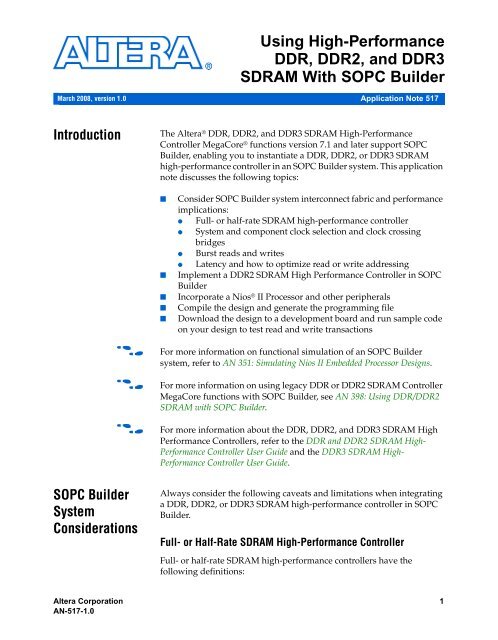
Using High-Performance DDR, DDR2, DDR3 SDRAM with SOPC ...
Using High-Performance DDR, DDR2, DDR3 SDRAM with SOPC ...
Using High-Performance DDR, DDR2, DDR3 SDRAM with SOPC ...

Create successful ePaper yourself
Turn your PDF publications into a flip-book with our unique Google optimized e-Paper software.
March 2008, version 1.0<br />
Introduction<br />
<strong>SOPC</strong> Builder<br />
System<br />
Considerations<br />
<strong>Using</strong> <strong>High</strong>-<strong>Performance</strong><br />
<strong>DDR</strong>, <strong>DDR</strong>2, and <strong>DDR</strong>3<br />
<strong>SDRAM</strong> With <strong>SOPC</strong> Builder<br />
Application Note 517<br />
The Altera ® <strong>DDR</strong>, <strong>DDR</strong>2, and <strong>DDR</strong>3 <strong>SDRAM</strong> <strong>High</strong>-<strong>Performance</strong><br />
Controller MegaCore ® functions version 7.1 and later support <strong>SOPC</strong><br />
Builder, enabling you to instantiate a <strong>DDR</strong>, <strong>DDR</strong>2, or <strong>DDR</strong>3 <strong>SDRAM</strong><br />
high-performance controller in an <strong>SOPC</strong> Builder system. This application<br />
note discusses the following topics:<br />
■ Consider <strong>SOPC</strong> Builder system interconnect fabric and performance<br />
implications:<br />
● Full- or half-rate <strong>SDRAM</strong> high-performance controller<br />
● System and component clock selection and clock crossing<br />
bridges<br />
● Burst reads and writes<br />
● Latency and how to optimize read or write addressing<br />
■ Implement a <strong>DDR</strong>2 <strong>SDRAM</strong> <strong>High</strong> <strong>Performance</strong> Controller in <strong>SOPC</strong><br />
Builder<br />
■ Incorporate a Nios ® II Processor and other peripherals<br />
■ Compile the design and generate the programming file<br />
■ Download the design to a development board and run sample code<br />
on your design to test read and write transactions<br />
f For more information on functional simulation of an <strong>SOPC</strong> Builder<br />
system, refer to AN 351: Simulating Nios II Embedded Processor Designs.<br />
f For more information on using legacy <strong>DDR</strong> or <strong>DDR</strong>2 <strong>SDRAM</strong> Controller<br />
MegaCore functions <strong>with</strong> <strong>SOPC</strong> Builder, see AN 398: <strong>Using</strong> <strong>DDR</strong>/<strong>DDR</strong>2<br />
<strong>SDRAM</strong> <strong>with</strong> <strong>SOPC</strong> Builder.<br />
f For more information about the <strong>DDR</strong>, <strong>DDR</strong>2, and <strong>DDR</strong>3 <strong>SDRAM</strong> <strong>High</strong><br />
<strong>Performance</strong> Controllers, refer to the <strong>DDR</strong> and <strong>DDR</strong>2 <strong>SDRAM</strong> <strong>High</strong>-<br />
<strong>Performance</strong> Controller User Guide and the <strong>DDR</strong>3 <strong>SDRAM</strong> <strong>High</strong>-<br />
<strong>Performance</strong> Controller User Guide.<br />
Always consider the following caveats and limitations when integrating<br />
a <strong>DDR</strong>, <strong>DDR</strong>2, or <strong>DDR</strong>3 <strong>SDRAM</strong> high-performance controller in <strong>SOPC</strong><br />
Builder.<br />
Full- or Half-Rate <strong>SDRAM</strong> <strong>High</strong>-<strong>Performance</strong> Controller<br />
Full- or half-rate <strong>SDRAM</strong> high-performance controllers have the<br />
following definitions:<br />
Altera Corporation 6.1 1<br />
AN-517-1.0 Preliminary
<strong>Using</strong> <strong>High</strong>-<strong>Performance</strong> <strong>DDR</strong>, <strong>DDR</strong>2, and <strong>DDR</strong>3 <strong>SDRAM</strong> With <strong>SOPC</strong> Builder<br />
■ Full-rate controllers present data to the local interface at twice the<br />
width of the actual <strong>SDRAM</strong> interface at the full <strong>SDRAM</strong> clock rate.<br />
■ Half-rate controllers present data to the local interface at four times<br />
the width of the actual <strong>SDRAM</strong> interface at half the <strong>SDRAM</strong> clock<br />
rate.<br />
Implementing the <strong>SDRAM</strong> high-performance controllers in half-rate<br />
mode gives the highest possible <strong>SDRAM</strong> clock frequency while allowing<br />
the more complex core logic to operate at half this frequency. You can<br />
simplify the complexity of your design by permitting your Nios II<br />
processor to run at the slower, half-rate memory speed while still<br />
achieving the required <strong>SDRAM</strong> bandwidth per I/O pin.<br />
However, where possible it is generally more optimal to configure the<br />
controller in full-rate mode <strong>with</strong> the core operating at the same clock<br />
frequency as your <strong>SOPC</strong> Builder system.<br />
Full-Rate Versus Half-Rate Command Operation<br />
Comamnds can be slower using a half-rate controller. For example, a<br />
<strong>DDR</strong> <strong>SDRAM</strong> device can have a number of banks open at once. Each bank<br />
has a currently selected row. Changing the column <strong>with</strong>in the selected<br />
row of an open bank requires no additional bank management<br />
commands to be issued. Changing the row in an active bank, or changing<br />
the bank both incur a protocol penalty that requires the precharge (PCH)<br />
command closes the active row or bank, and the active (ACT) command<br />
then opens (or activates) the new row or bank combination.<br />
The duration of this penalty is a function of the controller clock frequency,<br />
the memory clock frequency, and the memory device characteristics.<br />
Calculating the impact of a change of memory and controller<br />
configuration on a given system is not a trivial task, as it depends on the<br />
nature of the accesses that are performed.<br />
In this example each command takes a single clock cycle in a full-rate<br />
controller, but two clock cycles in a half-rate controller. The bank is not<br />
available for the subsequent ACT command until (tRP) after the PCH. So<br />
the issuing of commands can be slower using a half-rate controller, even<br />
if the respective memory timing parameters remain the same.<br />
Time-Specified Memory Parameters<br />
For a half-rate <strong>SDRAM</strong> high-performance controller, the control circuitry<br />
is clocked at half rate and so control operations are slower than in full-rate<br />
mode. However, the memory's clock frequency and physical properties<br />
are not affected.<br />
2 6.1 Altera Corporation<br />
Preliminary
<strong>SOPC</strong> Builder System Considerations<br />
When you use half-rate mode, any time-specified memory parameters in<br />
the controller are modified.<br />
For example, if:<br />
tRCDmin = 20 ns<br />
For a 133-MHz controller:<br />
tCK = 7.5 ns<br />
20/7.5 = 2.666 rounded up to 3 clock cycles (22.5ns).<br />
For a half-rate 66-MHz controller:<br />
tCK = 15 ns<br />
20/15 = 1.33 rounded up to 2 clock cycles (30ns).<br />
Thus bank and row changes are slower in half-rate mode, but are not<br />
twice as slow. The easiest way to measure this effect for your chosen<br />
memory device and interface clock speed is to simulate both half-rate and<br />
full-rate designs and record the increased latency when switching rows.<br />
Typically a full-rate controller is around 14% more efficient when<br />
switching rows <strong>with</strong>in a bank. As a half-rate controller has less read<br />
latency and if the masters in your system do not cause bank switching to<br />
occur often, the half-rate controller still gives higher performance. In<br />
<strong>SOPC</strong> Builder, you can alter arbitration shares to prevent masters from<br />
switching memory banks, thus creating a more optimal system.<br />
Clock Selection and Clock Crossing Bridges<br />
Ideally every component in the <strong>SOPC</strong> Builder system should be clocked<br />
using the same clock, to prevent <strong>SOPC</strong> Builder automatically adding<br />
clock domain crossing logic, which adds latency. The <strong>SDRAM</strong> highperformance<br />
controllers already include a PLL, so you should set the<br />
<strong>SOPC</strong> Builder system clock to altmemddr.sysclk, which is the clock<br />
the controller and local interface logic use. <strong>SOPC</strong> Builder only shows the<br />
input clock to the controller PLL, not the interface clock, see Figure 1.<br />
Altera Corporation 6.1 3<br />
Preliminary
<strong>Using</strong> <strong>High</strong>-<strong>Performance</strong> <strong>DDR</strong>, <strong>DDR</strong>2, and <strong>DDR</strong>3 <strong>SDRAM</strong> With <strong>SOPC</strong> Builder<br />
Figure 1. <strong>SOPC</strong> Builder Avalon-MM Slave and Master Clock Selection Note (1)<br />
Notes to Figure 1:<br />
(1) The clk clock is the input clock to the controller PLL.<br />
(2) The s1 clock is not stated, but is on the altmemddr.sysclk clock domain, not on the clk domain.<br />
If a different Avalon ® memory-mapped (Avalon-MM) clock is specified<br />
for connected components, <strong>SOPC</strong> Builder automatically adds clock<br />
crossing adapters between any data masters of your <strong>SOPC</strong> Builder<br />
system and the <strong>SDRAM</strong> high-performance controller slave interface.<br />
Clock crossing adapters provide robust and safe transactions between<br />
different clock domains, however they increase latency and limit total<br />
bandwidth.<br />
To prevent <strong>SOPC</strong> Builder from auto-inserting clock adapters:<br />
Avalon Slave s1 Clock<br />
(not stated, see Note 2)<br />
Avalon Master<br />
and Slave Clocks<br />
■ If the connected <strong>SOPC</strong> Builder components and <strong>SDRAM</strong> highperformance<br />
controller operate at the same frequency, use<br />
altmemddr.sysclk as the clock for the rest of your system. No<br />
clock domain crossing adapters are added by <strong>SOPC</strong> Builder.<br />
4 6.1 Altera Corporation<br />
Preliminary
<strong>SOPC</strong> Builder System Considerations<br />
■ If connected <strong>SOPC</strong> Builder components and <strong>SDRAM</strong> highperformance<br />
controller operate at different frequencies, manually<br />
insert an Avalon-MM clock crossing bridge between the <strong>SDRAM</strong><br />
high-performance controller and the other <strong>SOPC</strong> Builder<br />
components.<br />
To use the Avalon-MM clock crossing bridge, set its slave clock to your<br />
<strong>SOPC</strong> Builder system clock, and its master clock to altmemddr.sysclk.<br />
This component uses a FIFO for decoupling clock domains and is much<br />
more bandwidth efficient than the auto-inserted bridge. Size and<br />
structure of the bridge can be parameterized to implement a solution that<br />
is better optimized <strong>with</strong> lower latency.<br />
f For more information, refer to the Clock Domain Crossing section in the<br />
System Interconnect Fabric for Memory-Mapped Interfaces chapter and the<br />
Avalon Memory-Mapped Bridges chapter in the Quartus II Handbook.<br />
1 The Avalon-MM clock crossing bridge also works when you are<br />
using two different clocks at the same frequency but <strong>with</strong><br />
different phases.<br />
Use the Avalon-MM clock crossing bridge to allow a full-rate controller to<br />
connect to a half-rate <strong>SOPC</strong> builder design. The memory controller can<br />
still operate at a full-rate twice the Nios II frequency. So the memory<br />
interface commands operate at the faster rate. Figure 2 shows a clock<br />
crossing bridge example.<br />
Altera Corporation 6.1 5<br />
Preliminary
<strong>Using</strong> <strong>High</strong>-<strong>Performance</strong> <strong>DDR</strong>, <strong>DDR</strong>2, and <strong>DDR</strong>3 <strong>SDRAM</strong> With <strong>SOPC</strong> Builder<br />
Figure 2. Clock Crossing Bridge<br />
Nios II<br />
Processor<br />
M M<br />
Burst Reads and Writes<br />
Table 1 shows the burst length support for each type of <strong>SDRAM</strong> highperformance<br />
controller.<br />
Table 1. Burst Length Support<br />
M<br />
S<br />
JTAG<br />
UART<br />
S<br />
DMA<br />
Controller<br />
M M<br />
Arbiter Arbiter<br />
Clock-<br />
Crossing<br />
Bridge<br />
M<br />
Memory Type Full-Rate Mode Half-Rate Mode<br />
<strong>DDR</strong>3 — 8<br />
<strong>DDR</strong>2 4 4<br />
<strong>DDR</strong> 2 or 4 4<br />
Burst reads and writes differ in the following ways:<br />
■ In half-rate mode, the Avalon-MM slave interface is four times the<br />
width of the <strong>SDRAM</strong> device. Hence four transactions are performed<br />
on the <strong>SDRAM</strong> for every single Avalon-MM transaction. Avalon-MM<br />
burst requests on the local side serve no purpose as the memory<br />
interface is already using the maximum supported memory burst<br />
size for every single Avalon-MM transaction.<br />
6 6.1 Altera Corporation<br />
Preliminary<br />
S<br />
On-Chip<br />
Memory<br />
75 MHz<br />
150 MHz<br />
Avalon-MM Slave<br />
Interface<br />
PIO<br />
Avalon-MM Master<br />
Interface<br />
S<br />
S<br />
S<br />
<strong>SDRAM</strong><br />
Controller
<strong>SOPC</strong> Builder System Considerations<br />
■ In full-rate mode, you can use Avalon-MM bursts of one or two <strong>with</strong><br />
the <strong>SDRAM</strong> high-performance controller, as each Avalon-MM<br />
transaction results in only two <strong>SDRAM</strong> transactions. So two Avalon-<br />
MM burst transactions may be combined to support the four<br />
supported on the <strong>SDRAM</strong> high-performance controller.<br />
1 When a burst capable master supports larger burst lengths<br />
than the slave, <strong>SOPC</strong> Builder automatically places a burst<br />
length adapter into the path.<br />
To obtain performance advantages, ensure that the data widths of master<br />
and slave pairs are matched in <strong>SOPC</strong> Builder. Whenever a master port is<br />
connected to a slave port of a different width, <strong>SOPC</strong> Builder<br />
automatically inserts adapter logic to convert between the different data<br />
widths.<br />
Ideally, the data size of an Avalon-MM interface is 32 bits for a Nios II<br />
processor:<br />
■ For a full-rate <strong>SDRAM</strong> high-performance controller, the double-data<br />
rate stage doubles the data width, thus a 16-bit external memory<br />
width is best.<br />
■ For a half-rate <strong>SDRAM</strong> high-performance controller, the double-data<br />
rate and half-rate stages both double the data width, thus an 8-bit<br />
external memory width is best.<br />
Ideally, match the following data cache line sizes to the memory<br />
controller burst length:<br />
■ 4-byte line = bursts of 1 (32-bit word)<br />
■ 16-byte line = bursts of 4<br />
■ 32-byte line = bursts of 8<br />
You can set the data bus arbitration priority to avoid using the burst<br />
signal.<br />
Multimasters<br />
To achieve best throughput and latency of the <strong>SDRAM</strong>, you should<br />
connect the controller to the smallest number of masters and share those<br />
masters <strong>with</strong> the smallest number of slaves. Fewer connections reduce the<br />
complexity of the <strong>SOPC</strong> Builder auto-inserted data multiplexers and<br />
increase the f MAX of the Avalon-MM interface.<br />
1 If the Avalon-MM interface f MAX becomes the limiting factor,<br />
insert pipeline bridges to increase f MAX the (at the expense of<br />
latency).<br />
Altera Corporation 6.1 7<br />
Preliminary
<strong>Using</strong> <strong>High</strong>-<strong>Performance</strong> <strong>DDR</strong>, <strong>DDR</strong>2, and <strong>DDR</strong>3 <strong>SDRAM</strong> With <strong>SOPC</strong> Builder<br />
Master and slave pairs are locked for the whole duration of a burst—no<br />
other master is granted access to the slave target of a burst until the burst<br />
is completed. You should isolate critical memory connections from the<br />
rest of the system.<br />
One master may lock an <strong>SDRAM</strong> high-performance controller until a<br />
write burst is completed, which may take several cycles of time, during<br />
which the <strong>SDRAM</strong> high-performance controller cannot accept any other<br />
request. The write burst command is complete when all burst data is<br />
passed to the <strong>SDRAM</strong> high-performance controller. For a read burst, the<br />
controller quickly transfers back the whole burst at full bandwidth and<br />
becomes immediately available for new requests.<br />
Read and Write Addressing and Latency<br />
Systems <strong>with</strong> deterministic access patterns can minimize the number of<br />
bank and row changes. For example, by suitably arranging the memory<br />
map. In systems <strong>with</strong> more random access patterns (often typical in<br />
embedded <strong>SOPC</strong> Builder-type systems), minimizing bank and row<br />
changes is more difficult and the increased latency (by constantly<br />
changing the row in an active bank, or changing the bank) has a greater<br />
effect. Non-optimal cache implementations can waste cycles <strong>with</strong> halfrate<br />
controllers.<br />
You should always consider the following actions:<br />
■ Match controller Avalon-MM interface width to Avalon-MM master<br />
interface width.<br />
■ Minimize non-sequential addressing to reduce row addressing time.<br />
■ Match the Nios II cache line size to memory burst length.<br />
■ Set arbitration priorities correctly.<br />
■ Insert bridges to increase f MAX at the expense of latency.<br />
■ Minimize multimaster designs where arbitration stalls may take<br />
place.<br />
1 In multi-mastering designs, the memory is not available to<br />
all masters concurrently.<br />
Setting the arbitration priorities correctly prevents unnecessary memory<br />
accesses. For example, always set the Nios II instruction master<br />
arbitration priority to eight, because it always tries to access eight<br />
sequential addresses. Set the data master arbitration priorities depending<br />
on the cache line size; do not leave the arbitration priority value as<br />
default.<br />
8 6.1 Altera Corporation<br />
Preliminary
<strong>DDR</strong>2 <strong>SDRAM</strong><br />
<strong>High</strong>-<br />
<strong>Performance</strong><br />
Controller <strong>with</strong><br />
<strong>SOPC</strong> Builder<br />
Walkthrough<br />
<strong>DDR</strong>2 <strong>SDRAM</strong> <strong>High</strong>-<strong>Performance</strong> Controller <strong>with</strong> <strong>SOPC</strong> Builder Walkthrough<br />
This application note assumes that you are familiar <strong>with</strong> the Quartus ® II<br />
software and <strong>SOPC</strong> Builder. To use this application note, ensure you have<br />
the following software on your computer:<br />
■ Quartus ® II version 7.2<br />
■ ModelSim-Altera 6.1g or higher<br />
■ <strong>DDR</strong>2 <strong>SDRAM</strong> <strong>High</strong>-<strong>Performance</strong> Controller v7.2<br />
■ Nios II Embedded Design Suite (EDS) version 7.2<br />
The design is targeted to the Cyclone ® III FPGA Development Kit. You<br />
can target other supported device families or development kits.<br />
f For more information on the Cyclone III FPGA Development Kit, refer to<br />
www.altera.com/products/devkits/altera/kit-cyc3.html.<br />
Create Your Example Project<br />
This section shows you how to create a new Quartus II project and an<br />
<strong>SOPC</strong> Builder system.<br />
Create a New Quartus II Project<br />
In the Quartus II software, create a new project <strong>with</strong> the New Project<br />
Wizard, ensure that the device type is set to Cyclone III, EP3C120F780C7.<br />
1 Ensure that your project path does not include any spaces or<br />
extended characters.<br />
Create the <strong>SOPC</strong> Builder System<br />
To create an <strong>SOPC</strong> Builder system, follow these steps:<br />
1. On the Tools menu click <strong>SOPC</strong> Builder.<br />
2. In the Create New System dialog box, enter sopc_top for the<br />
System Name. In the Target HDL, select Verilog, then click OK.<br />
3. On the System Contents tab expand Memories and Memory<br />
Controllers. Expand <strong>SDRAM</strong>. Select <strong>DDR</strong>2 <strong>SDRAM</strong> <strong>High</strong><br />
<strong>Performance</strong> Controller and click Add. The <strong>DDR</strong>2 <strong>SDRAM</strong> highperformance<br />
controller wizard opens.<br />
4. For the Speed Grade, select 7, to match the chosen device.<br />
5. For the PLL reference clock frequency, enter 50 MHz, to match<br />
signal CLKIN50.<br />
Altera Corporation 6.1 9<br />
Preliminary
<strong>Using</strong> <strong>High</strong>-<strong>Performance</strong> <strong>DDR</strong>, <strong>DDR</strong>2, and <strong>DDR</strong>3 <strong>SDRAM</strong> With <strong>SOPC</strong> Builder<br />
6. For the Memory clock frequency, enter 150 MHz.<br />
1 150 MHz is the maximum supported frequency for <strong>DDR</strong>2, SSTL-<br />
18 class I, in top and bottom I/O, in a C7 speed grade Cyclone III<br />
device.<br />
7. For the Local interface clock frequency, select Half.<br />
8. For the Memory vendor, select Micron.<br />
9. For the Memory format, select Discrete Device.<br />
10. For the Memory Presets, select Micron MT47H32M16CC-3 x4 +<br />
MT47H32M8BP-3 x1 (see Figure 3).<br />
1 This memory preset has been included by Altera in the <strong>DDR</strong>2<br />
<strong>SDRAM</strong> high-performance controller as it matches the exact<br />
configuration that both the Cyclone III development board and<br />
the Stratix II GX PCIe Development Kit use.<br />
10 6.1 Altera Corporation<br />
Preliminary
Figure 3. Memory Settings<br />
<strong>DDR</strong>2 <strong>SDRAM</strong> <strong>High</strong>-<strong>Performance</strong> Controller <strong>with</strong> <strong>SOPC</strong> Builder Walkthrough<br />
11. Click Modify parameters and ensure you change the following<br />
parameters:<br />
● Output clock pairs from FPGA, select 1 pairs<br />
● Memory interface DQ width, select 8 bits, to give in an Avalon-<br />
MM width of 32 bits, which is ideal to connect to a Nios II<br />
processor<br />
● Memory drive strength setting, select Reduced (DQ are low<br />
load point-to-point connections)<br />
Altera Corporation 6.1 11<br />
Preliminary
<strong>Using</strong> <strong>High</strong>-<strong>Performance</strong> <strong>DDR</strong>, <strong>DDR</strong>2, and <strong>DDR</strong>3 <strong>SDRAM</strong> With <strong>SOPC</strong> Builder<br />
● Memory on-die termination (ODT) setting, select Disabled<br />
(discrete class I termination is already fitted to the development<br />
board)<br />
● Memory CAS latency setting, select 3.0 cycles (this <strong>DDR</strong>2<br />
<strong>SDRAM</strong> supports CAS = 3 for frequencies of 200 MHz or lower)<br />
12. Click OK then click Finish in the <strong>DDR</strong>2 <strong>SDRAM</strong> high-performance<br />
controller wizard.<br />
Figure 4. Preset Editor<br />
Add <strong>SOPC</strong> Builder Components<br />
To add components from the System Contents tab, follow these steps:<br />
12 6.1 Altera Corporation<br />
Preliminary
<strong>DDR</strong>2 <strong>SDRAM</strong> <strong>High</strong>-<strong>Performance</strong> Controller <strong>with</strong> <strong>SOPC</strong> Builder Walkthrough<br />
1. Expand On-Chip Memory and select On-Chip Memory, click Add.<br />
For Total memory size enter 64 KBytes. Click Finish.<br />
2. Select On-Chip Memory again, click Add.<br />
a. Set Total memory size to 4096 Bytes.<br />
b. Select Finish.<br />
c. Right click on this second on-chip memory, click Rename and<br />
type dma_read_memory and press Enter.<br />
3. On the System menu, click Auto-Assign Base Addresses.<br />
4. Select Nios II Processor and click Add.<br />
a. Select Nios II/s.<br />
b. For Reset Vector and Exception Vector select onchip_mem. If<br />
local on-chip memory holds the Nios II instruction code, less<br />
arbitration is required to the <strong>SDRAM</strong> interface resulting in a<br />
more optimal Avalon-MM structure.<br />
c. Change Reset Vector Offset to 0x20 and Exception Vector<br />
Offset to 0x40.<br />
c The controller performs memory interface calibration every<br />
time it is reset and in doing so writes to addresses 0x0 to 0x1f.<br />
If you want your memory contents to remain intact through a<br />
system reset, you should avoid using the memory addresses<br />
below 0x20. This step is not necessary, if you reload your<br />
<strong>SDRAM</strong> contents from flash every time you reset.<br />
d. Click Finish.<br />
5. Expand Interface Protocols and expand Serial, select JTAG UART<br />
and click Add.<br />
a. For both the read and write FIFO, for the Buffer Depth (bytes)<br />
select 64 and for IRQ threshold enter 8.<br />
b. Click Finish.<br />
6. Expand Peripherals and expand Microcontroller Peripherals,<br />
select PIO (Parallel I/O), click Add.<br />
a. For the Width enter 8 bits.<br />
Altera Corporation 6.1 13<br />
Preliminary
<strong>Using</strong> <strong>High</strong>-<strong>Performance</strong> <strong>DDR</strong>, <strong>DDR</strong>2, and <strong>DDR</strong>3 <strong>SDRAM</strong> With <strong>SOPC</strong> Builder<br />
b. For Direction select Output ports only.<br />
c. Click Finish.<br />
7. Expand Memories and Memory Controllers and expand DMA,<br />
select DMA Controller and click Add.<br />
a. Turn on Enable burst transfers, for the Maximum burst size<br />
select 512 words.<br />
b. Click the Advanced tab. Turn off doubleword and quadword<br />
on the Advanced tab.<br />
c. Click Finish.<br />
1 Do not to add a PLL component to your <strong>SOPC</strong> Builder design as<br />
the <strong>DDR</strong>2 <strong>SDRAM</strong> high-performance controller includes one.<br />
8. Set the bus links (see Figure 5).<br />
a. Connect the DMA read_master and write_master to both the<br />
altmemddr and the dma_read_memory.<br />
1 If there are warnings about overlapping addresses, on the<br />
System menu click Auto-Assign Base Addresses.<br />
1 If there are warnings about overlapping IRQ, on the System<br />
menu click Auto-Assign IRQs.<br />
b. Ensure that altmemddr is clocked on the external clock clk and<br />
that the frequency matches the external oscillator (50 MHz for<br />
the Cyclone III development board).<br />
c. Ensure that all other modules are clocked on the<br />
altmemddr_sysclk, to avoid any unnecessary clock-domain<br />
crossing logic.<br />
f For more information on <strong>SOPC</strong> Builder system interconnect fabric, refer<br />
to the System Interconnect Fabric for Memory-Mapped Interfaces chapter in<br />
the Quartus II Handbook.<br />
14 6.1 Altera Corporation<br />
Preliminary
Figure 5. <strong>SOPC</strong> Builder Final System Connection<br />
<strong>DDR</strong>2 <strong>SDRAM</strong> <strong>High</strong>-<strong>Performance</strong> Controller <strong>with</strong> <strong>SOPC</strong> Builder Walkthrough<br />
Generate the <strong>SOPC</strong> Builder System<br />
To generate the system, follow these steps:<br />
1. In <strong>SOPC</strong> Builder, click Next.<br />
2. Turn off Simulation. Create simulator project files.<br />
f For more information on <strong>SOPC</strong> simulation and testbench options, refer<br />
to Volume 4: <strong>SOPC</strong> Builder of the Quartus II Handbook and AN 351:<br />
Simulating Nios II Systems.<br />
3. In <strong>SOPC</strong> Builder, click Generate. Click Save. When the generation is<br />
finished you see the following message:<br />
SUCCESS: SYSTEM GENERATION COMPLETED.<br />
4. In <strong>SOPC</strong> Builder, click Exit.<br />
Altera Corporation 6.1 15<br />
Preliminary
<strong>Using</strong> <strong>High</strong>-<strong>Performance</strong> <strong>DDR</strong>, <strong>DDR</strong>2, and <strong>DDR</strong>3 <strong>SDRAM</strong> With <strong>SOPC</strong> Builder<br />
Create the Top-Level Design File<br />
Figure 6. <strong>SOPC</strong> Builder Top-Level Block Diagram<br />
global_reset<br />
clock_source<br />
Conceptually, you can consider the <strong>SOPC</strong> Builder system as component<br />
in your design. It can be the only component; or one of many components.<br />
Hence, when your <strong>SOPC</strong> Builder system is complete, you must add it to<br />
your top-level design.<br />
The top-level design can be in your preferred HDL language, or simply a<br />
.bdf schematic design.<br />
In this walkthrough, the top-level design is a simple wrapper file around<br />
the <strong>SOPC</strong> Builder system <strong>with</strong> no additional components. The top-level<br />
design file just defines the pin naming convention and port connections.<br />
Figure 6 shows the <strong>SOPC</strong> Builder top-level block diagram.<br />
reset<br />
global_reset<br />
Top-Level Design File<br />
Nios II<br />
Processor<br />
On-Chip<br />
Memory<br />
sopc_top<br />
JTAG<br />
UART<br />
DMA<br />
Controller<br />
The <strong>SDRAM</strong> high-performance controller needs to make assignments to<br />
the top-level memory interface pins. These assignments are applied <strong>with</strong><br />
the autogenerated script and constraint files. To ensure the constraints<br />
work, you must ensure the pin names and pin group assignments match,<br />
otherwise you get a no fit when you compile your design. The pin names<br />
default to mem_*. You can see the expected default pin names in the<br />
generated altmemddr_example_top file. You may optionally apply a<br />
prefix to the default pin naming convention.<br />
All the <strong>SDRAM</strong> high-performance controllers generate the standalone<br />
example design altmemddr_example_top. This file only includes the<br />
controller and an example driver (see Figure 7). This file does not<br />
instantiate your <strong>SOPC</strong> Builder system but you can use the file in one of<br />
the following ways:<br />
■ Identify the default memory controller pin names<br />
■ Use as a starting point for the rest of the design<br />
16 6.1 Altera Corporation<br />
Preliminary<br />
PIO<br />
<strong>SDRAM</strong><br />
Controller<br />
<strong>SDRAM</strong><br />
Interface<br />
PIO
<strong>DDR</strong>2 <strong>SDRAM</strong> <strong>High</strong>-<strong>Performance</strong> Controller <strong>with</strong> <strong>SOPC</strong> Builder Walkthrough<br />
Figure 7. Example Design<br />
Example Design<br />
Example Driver<br />
Local<br />
Interface<br />
Control<br />
Logic<br />
(Encrypted)<br />
ALTMEMPHY<br />
Megafunction<br />
<strong>DDR</strong>2 <strong>SDRAM</strong><br />
<strong>High</strong>-<strong>Performance</strong><br />
Controller<br />
<strong>DDR</strong>2 <strong>SDRAM</strong><br />
Interface<br />
You can create a HDL top-level design using the<br />
altmemddr_example_top as a template. You may edit the pin names (if<br />
required) in the altmemddr_example_top file only <strong>with</strong> the addition of a<br />
prefix. You must replace the example driver and the <strong>DDR</strong>2 <strong>SDRAM</strong> highperformance<br />
controller and instantiate your <strong>SOPC</strong> Builder-generated<br />
system.<br />
As a reference, Altera provides an example.bdf top-level design <strong>with</strong> the<br />
correct pin names (see Figure 8). The mem_clk[0] and mem_clk_n[0]<br />
pins are bidirectional (because of the mimic path in the ALTMEMPHY<br />
megafunction).<br />
Altera Corporation 6.1 17<br />
Preliminary
<strong>Using</strong> <strong>High</strong>-<strong>Performance</strong> <strong>DDR</strong>, <strong>DDR</strong>2, and <strong>DDR</strong>3 <strong>SDRAM</strong> With <strong>SOPC</strong> Builder<br />
Figure 8. Quartus II Top-Level Project<br />
To create a top-level design for your <strong>SOPC</strong> Builder system using a<br />
Quartus II .bdf schematic, follow these steps:<br />
1. In the Quartus II software, on the File menu click New.<br />
2. Select Block Diagram/Schematic File and click OK. A blank .bdf,<br />
Block1.bdf, opens.<br />
3. On the File menu click Save As. In the Save As dialog window, click<br />
Save.<br />
1 The Quartus II software automatically sets the .bdf file<br />
name to your project name.<br />
4. Right-click in the blank .bdf, point to Insert and click Symbol to<br />
open the Symbol dialog box.<br />
5. Under Libraries, expand Project, select sopc_top, click OK.<br />
6. Position the <strong>SOPC</strong> Builder system component outline in the<br />
.bdf and left-click.<br />
7. Right-click on the <strong>SOPC</strong> Builder system component and click<br />
Generate Pins for Symbol Ports, to automatically add pins and nets<br />
to the schematic symbol.<br />
18 6.1 Altera Corporation<br />
Preliminary
<strong>DDR</strong>2 <strong>SDRAM</strong> <strong>High</strong>-<strong>Performance</strong> Controller <strong>with</strong> <strong>SOPC</strong> Builder Walkthrough<br />
8. The autogenerated pin names match the <strong>SOPC</strong> Builder system pin<br />
names. Select each pin and manually change each pin name to<br />
match the equivalent pin name in altmemddr_example_top.<br />
1 The <strong>SOPC</strong> Builder system includes the following<br />
unrequired signals for this example design, which you can<br />
disconnect:<br />
altmemddr_phy_clk_out<br />
local_init_done_from_the_altmemddr<br />
local_refresh_ack_from_the_altmemddr<br />
local_wdata_req_from_the_altmemddr<br />
• reset_phy_clk_n_from_the_altmemddr<br />
1 The following single vector signals require a [0] vectored<br />
pin name, otherwise simulation may fail:<br />
• mem_dm<br />
• mem_dqs<br />
• mem_clk<br />
• mem_cke<br />
• mem_cs_n<br />
mem_odt<br />
9. The <strong>SOPC</strong> Builder System has two reset inputs, reset_n and<br />
global_reset_n_to_the_altmemddr. Connect both these<br />
signals to a single pin global_reset_n.<br />
10. Ensure you rename the clock signal to clock_source.<br />
f For more information on the signals, refer to the ALTMEMPHY<br />
Megafunction User Guide.<br />
11. Change the name of out_port_from_the_pio[7..0] to<br />
pio[7..0].<br />
14. On the File menu click Save, to save your changes.<br />
15. On the Project menu click Set as Top-Level Entity.<br />
Update the Quartus II Project Settings<br />
To ensure the Quartus II project obtains optimum results, follow these<br />
steps:<br />
1. On the Assignments menu click Settings. In the Category list, select<br />
Fitter Settings. For Fitter effort select Standard Fit (<strong>High</strong>est Effort).<br />
Altera Corporation 6.1 19<br />
Preliminary
<strong>Using</strong> <strong>High</strong>-<strong>Performance</strong> <strong>DDR</strong>, <strong>DDR</strong>2, and <strong>DDR</strong>3 <strong>SDRAM</strong> With <strong>SOPC</strong> Builder<br />
2. In the Category list, select Analysis and Synthesis Settings. For<br />
Optimization Technique select Speed.<br />
3. In the Category list, select Device. Click Device and Pin Options.<br />
Click the Unused Pins tab, for Reserve all unused pins select As<br />
input tri-stated <strong>with</strong> weak pull-up resistor.<br />
4. Click the Voltage tab, for Default I/O standard select the same<br />
VCCIO voltage as the chosen <strong>SDRAM</strong> interface; for <strong>DDR</strong>2 <strong>SDRAM</strong><br />
select 1.8 V. Click OK.<br />
5. In the Category list, select Timing Analysis Settings, select<br />
TimeQuest Timing Analyzer During Compilation.<br />
6. In the Category list, expand Timing Analysis Settings and select<br />
TimeQuest Timing Analyzer. Browse to the autogenerated<br />
altmemddr_phy_ddr_timing.sdc file and click Add. Click OK.<br />
Specify the Top-Level Design Pin Out<br />
Any <strong>DDR</strong> <strong>SDRAM</strong> interface must have its signals placed on the correct<br />
pin type and group. To specify the top-level design pin out, follow these<br />
steps:<br />
1. On the Processing menu, point to Start and click Start Analysis and<br />
Synthesis.<br />
2. Add pin I/O standard assignments:<br />
a. If you are using the default pin names, run<br />
_pin_assignments.tcl. On the Tools menu<br />
click Tcl Scripts, select _pin_ssignments.tcl<br />
and click Run.<br />
or<br />
b. If you require pins name changes (prefix changes only) use the<br />
Quartus II Pin Planner and Import an existing custom<br />
megafunction.<br />
On the Assignment menu click Pin Planner.<br />
Right-click in any area under Node Name and select<br />
Create/Import Megafunction (see Figure 9).<br />
Select Import an existing custom megafunction and select<br />
the .ppf file.<br />
Type the prefix that you want to use in Instance name (see<br />
Figure 10).<br />
20 6.1 Altera Corporation<br />
Preliminary
Figure 9. Create/Import Megafunction in Pin Planner<br />
<strong>DDR</strong>2 <strong>SDRAM</strong> <strong>High</strong>-<strong>Performance</strong> Controller <strong>with</strong> <strong>SOPC</strong> Builder Walkthrough<br />
Figure 10. Adding Prefix<br />
f For more information about the <strong>DDR</strong>, <strong>DDR</strong>2, and <strong>DDR</strong>3 <strong>SDRAM</strong> <strong>High</strong><br />
<strong>Performance</strong> Controllers pin naming, refer to the <strong>DDR</strong> and <strong>DDR</strong>2<br />
<strong>SDRAM</strong> <strong>High</strong>-<strong>Performance</strong> Controller User Guide and the <strong>DDR</strong>3 <strong>SDRAM</strong><br />
<strong>High</strong>-<strong>Performance</strong> Controller User Guide.<br />
Altera Corporation 6.1 21<br />
Preliminary
<strong>Using</strong> <strong>High</strong>-<strong>Performance</strong> <strong>DDR</strong>, <strong>DDR</strong>2, and <strong>DDR</strong>3 <strong>SDRAM</strong> With <strong>SOPC</strong> Builder<br />
3. Assign all of your pins, so the Quartus II software fits your design<br />
correctly and gives correct timing analysis. To assign pin locations<br />
for the Cyclone III development board, run the Altera-provided<br />
c3_host_ddr2_sopc_pins.tcl file or manually assign pin locations by<br />
using either the Pin Planner or Assignment Editor.<br />
1 The <strong>SDRAM</strong> high-performance controller autogenerated<br />
scripts do not make any pin location assignments.<br />
1 If you are at the design exploration phase of your design<br />
cycle and do not have any PCB defined pin locations, you<br />
should still manually define an initial set of pin constraints,<br />
which can become more specific during your development<br />
process.<br />
To manually assign pin locations, follow these steps:<br />
1. Open Pin Planner. On the Assignments menu, click Pin Planner.<br />
2. Assign DQ and DQS pins.<br />
a. To select the device DQS pin groups that the design uses, assign<br />
each DQS pin in your design to the required DQS pin in the Pin<br />
Planner. The Quartus II Fitter then automatically places the<br />
respective DQ signals onto suitable DQ pins <strong>with</strong>in each group.<br />
To see DQS groups in Pin Planner, right click, select Show<br />
DQ/DQS Pins, and click In x8/x9 Mode. Pin Planner shows<br />
each DQS group in a different color and <strong>with</strong> a different legend:<br />
S = DQS pin, Sbar = DQSn pin and Q = DQ pin (see Figure 11).<br />
1 Most <strong>DDR</strong>2 <strong>SDRAM</strong> devices operate in ×8/×9 mode,<br />
however as some <strong>DDR</strong>2 <strong>SDRAM</strong> devices operate in ×4<br />
mode, refer to your specific memory device datasheet.<br />
b. Select the DQ mode to match the DQ group width (number of<br />
DQ pins/number of DQS pins) of your memory device. DQ<br />
mode is not related to the memory interface width.<br />
1 DQ group order and DQ pin order <strong>with</strong>in each group is not<br />
important. However, you must place DQ pins in the same<br />
group as their respective strobe pin.<br />
22 6.1 Altera Corporation<br />
Preliminary
<strong>DDR</strong>2 <strong>SDRAM</strong> <strong>High</strong>-<strong>Performance</strong> Controller <strong>with</strong> <strong>SOPC</strong> Builder Walkthrough<br />
Figure 11. Quartus II Pin Planner, Show DQ/DQS Pins, In x8/x9 Mode<br />
3. Place DM pins <strong>with</strong>in their respective DQ group.<br />
4. Place address and control/command pins on any spare I/O pins<br />
ideally <strong>with</strong>in the same bank or side of the device as the mem_clk<br />
pins.<br />
5. Ensure mem_clk pins use any regular adjacent I/O pins—ideally<br />
differential I/O pairs for the CK/CK# pin pair. To identify<br />
differential I/O pairs, right-click in Pin Planner and select Show<br />
Differential Pin Pair Connections. Pin pairs show a red line<br />
between each pin pair.<br />
6. Place the clock_source pin on a dedicated PLL clock input pin<br />
<strong>with</strong> a direct connection to the <strong>SDRAM</strong> controller PLL/DLL pair—<br />
usually on the same side of the device as your memory interface.<br />
This recommendation reduces PLL jitter, saves a global clock<br />
resource, and eases timing and fitter effort.<br />
Altera Corporation 6.1 23<br />
Preliminary
<strong>Using</strong> <strong>High</strong>-<strong>Performance</strong> <strong>DDR</strong>, <strong>DDR</strong>2, and <strong>DDR</strong>3 <strong>SDRAM</strong> With <strong>SOPC</strong> Builder<br />
7. Place the global_reset_n pin (like any high fan-out signal) on a<br />
dedicated clock pin.<br />
f For more information on how to use the Quartus II Pin Planner, refer to<br />
the I/O Management chapter in volume 2 of the Quartus II Handbook.<br />
f For more information on Cyclone III external memory pin selection, refer<br />
to the External Memory Interface in Cyclone III Devices chapter in the<br />
Cyclone III Device Handbook.<br />
<strong>DDR</strong>2 <strong>SDRAM</strong> in Stratix III devices <strong>with</strong> differential DQS mode require<br />
mem_clk[0]/mem_clk_n[0] on a DIFFIO_RX capable pin pair. <strong>DDR</strong>3<br />
<strong>SDRAM</strong> interfaces in Stratix III devices require<br />
mem_clk[0]/mem_clk_n[0] in any DQ or DQS pin pair <strong>with</strong><br />
DIFFIO_RX capability.<br />
f For more information on Stratix III external memory pin selection, refer<br />
to External Memory Interfaces in Stratix III Devices chapter in the Stratix III<br />
Device Handbook.<br />
Compile the Design<br />
To compile the design, on the Processing menu click Start Compilation.<br />
Verify Memory Interface Timing<br />
To verify memory interface timing, follow these steps:<br />
1. On the Tools menu click Tcl Scripts.<br />
2. Select _phy_report_timing.tcl and click Run.<br />
Test the Design On A Development Platform<br />
To test the design on a development platform, follow these steps:<br />
■ “Add the SignalTap II Logic Analyzer” on page 24<br />
■ “Compile the Project” on page 27<br />
■ “Verify Timing” on page 28<br />
Add the SignalTap II Logic Analyzer<br />
The SignalTap II logic analyzer shows read and write activity in the<br />
system.<br />
f For more information on using the SignalTap II logic analyzer, refer to<br />
the following documents:<br />
24 6.1 Altera Corporation<br />
Preliminary
<strong>DDR</strong>2 <strong>SDRAM</strong> <strong>High</strong>-<strong>Performance</strong> Controller <strong>with</strong> <strong>SOPC</strong> Builder Walkthrough<br />
■ Design Debugging <strong>Using</strong> the SignalTap II Embedded Logic Analyzer<br />
chapter in the Quartus II Handbook<br />
■ AN 323: <strong>Using</strong> SignalTap II Embedded Logic Analyzers in <strong>SOPC</strong> Builder<br />
Systems<br />
■ AN 446: Debugging Nios II Systems <strong>with</strong> the SignalTap II Logic Analyzer<br />
To add the SignalTap II logic analyzer, follow these steps:<br />
1. On the Tools menu click SignalTap II Logic Analyzer.<br />
2. In the Signal Configuration window next to the Clock box, click …<br />
(Browse Node Finder).<br />
3. Type *phy_clk in the Named box, for Filter select SignalTap II:<br />
pre-synthesis and click List.<br />
4. Select sopc_top:inst|altmemddr:the_altmemddr|phy_clk in<br />
Nodes Found and click > to add the signal to Selected Nodes.<br />
5. Click OK.<br />
6. Under Signal Configuration, specify the following settings:<br />
● For Sample depth, select 512<br />
● For RAM type, select Auto (Stratix III devices only)<br />
● For Trigger flow control, select Sequential<br />
● For Trigger position, select Center trigger position<br />
● For Trigger conditions, select 1<br />
7. On the Edit menu, click Add Nodes.<br />
8. Search for specific nodes by typing *local* in the Named box, for<br />
Filter select SignalTap II: pre-synthesis and click List.<br />
9. Select the following nodes in Nodes Found and click > to add to<br />
Selected Nodes:<br />
● local_address<br />
● local_rdata<br />
● local_rdata_valid (alternative trigger to compare read/write<br />
data)<br />
● local_read_req<br />
● local_ready<br />
● local_wdata<br />
● local_wdata_req<br />
● local_write_req (trigger)<br />
Altera Corporation 6.1 25<br />
Preliminary
<strong>Using</strong> <strong>High</strong>-<strong>Performance</strong> <strong>DDR</strong>, <strong>DDR</strong>2, and <strong>DDR</strong>3 <strong>SDRAM</strong> With <strong>SOPC</strong> Builder<br />
1 Do not add any <strong>DDR</strong> <strong>SDRAM</strong> interface signals to the<br />
SignalTap II logic analyzer. The load on these signals<br />
increases and adversely affects the timing analysis.<br />
10. Click OK.<br />
11. To reduce the SignalTap II logic size, turn off Trigger Enable on the<br />
following bus signals:<br />
● local_address<br />
● local_rdata<br />
● local_wdata<br />
12. Right-click Trigger Conditions for the local_write_req signal<br />
and select Rising Edge.<br />
Figure 12 shows the completed SignalTap II logic analyzer.<br />
26 6.1 Altera Corporation<br />
Preliminary
Figure 12. SignalTap II Logic Analyzer<br />
<strong>DDR</strong>2 <strong>SDRAM</strong> <strong>High</strong>-<strong>Performance</strong> Controller <strong>with</strong> <strong>SOPC</strong> Builder Walkthrough<br />
13. On the File menu, click Save, to save the SignalTap II .stp file to your<br />
project.<br />
1 If you get the message Do you want to enable SignalTap II<br />
file “stp1.stp” for the current project, click Yes.<br />
Compile the Project<br />
Once you add signals to the SignalTap II logic analyzer, recompile your<br />
design, on the Processing menu click Start Compilation.<br />
Altera Corporation 6.1 27<br />
Preliminary
<strong>Using</strong> <strong>High</strong>-<strong>Performance</strong> <strong>DDR</strong>, <strong>DDR</strong>2, and <strong>DDR</strong>3 <strong>SDRAM</strong> With <strong>SOPC</strong> Builder<br />
Verify Timing<br />
Once the design compiles, ensure that TimeQuest timing analysis passes<br />
successfully. In addition to this FPGA timing analysis, check your PCB or<br />
system <strong>SDRAM</strong> timing. To run timing analysis, run the<br />
*_phy_report_timing.tcl script.<br />
1. On the Tools menu click Tcl Scripts.<br />
2. Select _phy_report_timing.tcl and click Run.<br />
Connect the Development Board<br />
Connect the Cyclone III development board to your computer.<br />
For more information on the Cyclone III development board, refer to the<br />
Cyclone III Development Kit User Guide.<br />
Download the Object File<br />
On the Tools menu, click SignalTap II Logic Analyzer. The SignalTap II<br />
dialog box appears.<br />
The SOF Manager should contain the .sof file. To add<br />
the correct file to the SOF Manager, follow these steps:<br />
1. Click ... to open the Select Program Files dialog box (see Figure 13).<br />
2. Select .sof.<br />
3. Click Open.<br />
4. To download the file, click the Program Device button (see<br />
Figure 13).<br />
Figure 13. Install the SRAM Object File in the SignalTap II Dialog Box<br />
Program Device Browse Program Files<br />
28 6.1 Altera Corporation<br />
Preliminary
<strong>DDR</strong>2 <strong>SDRAM</strong> <strong>High</strong>-<strong>Performance</strong> Controller <strong>with</strong> <strong>SOPC</strong> Builder Walkthrough<br />
Incorporate the Nios II IDE<br />
You can now add test code to the project’s Nios II processor and use this<br />
program to run some simple tests.<br />
When doing memory tests, you must read and write from the external<br />
<strong>DDR</strong> <strong>SDRAM</strong> and not from cached memory. The following three<br />
methods avoid using Nios II cached memory:<br />
■ Use a Nios II processor that does not have cache memory, like the<br />
Nios II/s used in this example project.<br />
■ Use the alt_remap_uncached function.<br />
Launch Nios II IDE<br />
To launch the Nios II IDE, follow these steps:<br />
1. One the Tools menu, click <strong>SOPC</strong> Builder.<br />
2. Click the System Generation tab.<br />
3. Click Nios II IDE.<br />
1 If it is the first time you have run the IDE, click Workbench.<br />
4. On the File menu click Switch Workspace and select your project<br />
directory.<br />
5. On the File menu point to New and click Project.<br />
6. Expand Altera Nios II select Nios II C/C++ Application and click<br />
Next.<br />
7. Select Blank Project under Select Project Templates and click Next.<br />
8. Ensure that <strong>SOPC</strong> Builder System .ptf is /.ptf.<br />
9. Click Next and click Finish.<br />
10. In Windows Explorer drag Altera-supplied main.c to the<br />
blank_project_0 directory.<br />
f To see the main.c example test program, see “Appendix: Example main.c<br />
Test Program File” on page 39.<br />
Altera Corporation 6.1 29<br />
Preliminary
<strong>Using</strong> <strong>High</strong>-<strong>Performance</strong> <strong>DDR</strong>, <strong>DDR</strong>2, and <strong>DDR</strong>3 <strong>SDRAM</strong> With <strong>SOPC</strong> Builder<br />
Table 2. Commands<br />
This program consists of a simple loop that takes commands from the<br />
JTAG UART and executes them. Table 2 shows the commands that are<br />
sent to the Nios II C code.<br />
1 The commands must be in the following format and the<br />
switches A,B,C, and D must be entered in upper case. Both<br />
address and data strings must always be 8 characters long.<br />
Command Format Description Example<br />
Switch A Switch | Data Controls the LEDs. A000000FF. The last two<br />
bytes control all eight LEDs.<br />
The LEDs are active low on<br />
the board.<br />
Switch B Switch | Address | Data Performs a single write to an<br />
address offset location in<br />
memory.<br />
Switch C Switch | Address Performs a single read to an<br />
address offset location in<br />
memory.<br />
Switch D Switch | From Address | To Address Performs an incremental<br />
write to the first address<br />
location, followed by a DMA<br />
burst transfer from the first<br />
address location to the<br />
second address location.<br />
The burst is a fixed length of<br />
512 words or 2048 bytes.<br />
Enter B, followed by<br />
00000000, then<br />
00000001, writes<br />
00000001 at <strong>SDRAM</strong><br />
address offset location<br />
00000000.<br />
Enter C, followed by<br />
00000000, reads the<br />
contents of the memory at<br />
<strong>SDRAM</strong> address offset<br />
location 00000000.<br />
D0200100000000000<br />
loads the DMA read<br />
memory <strong>with</strong> the<br />
incrementing pattern, then<br />
DMA burst transfers it to the<br />
<strong>SDRAM</strong> high-performance<br />
controller.<br />
You can read the <strong>SOPC</strong> Builder component address locations directly<br />
from the <strong>SOPC</strong> Builder Window (see Figure 14).<br />
30 6.1 Altera Corporation<br />
Preliminary
Figure 14. <strong>SOPC</strong> Builder Component Address<br />
<strong>DDR</strong>2 <strong>SDRAM</strong> <strong>High</strong>-<strong>Performance</strong> Controller <strong>with</strong> <strong>SOPC</strong> Builder Walkthrough<br />
<strong>SDRAM</strong><br />
Start Address<br />
Setup the Project Settings<br />
Burst DMA<br />
Start Address<br />
To setup the Nios II project settings, follow these steps:<br />
1. In the Nios II C/C++ Projects tab right-click blank_project_0 and<br />
click System Library Properties.<br />
2. Click System Library in the list on the left side of the Properties<br />
dialog box.<br />
3. To optimize the footprint size of the library project, under System<br />
Library Contents, turn on Reduced device drivers.<br />
4. Under Linker Script, for all the memory options select<br />
onchip_mem. The on-chip memory is the target memory space for<br />
the executable file.<br />
5. To reduce the memory size allocated for the system library, for Max<br />
file descriptors enter 4. Figure 15 shows the Properties dialog box.<br />
Altera Corporation 6.1 31<br />
Preliminary
<strong>Using</strong> <strong>High</strong>-<strong>Performance</strong> <strong>DDR</strong>, <strong>DDR</strong>2, and <strong>DDR</strong>3 <strong>SDRAM</strong> With <strong>SOPC</strong> Builder<br />
Figure 15. Nios II Project Settings<br />
6. Click OK.<br />
7. Right click on blank_project_0, point to Run As, and click Nios II<br />
Hardware.<br />
The Nios II C/C++ IDE compiles the example test program.<br />
If you have more than one JTAG download cable connected to your<br />
computer you may see an JTAG error. If you receive a JTAG error, follow<br />
these steps:<br />
1. From the Nios II IDE, on the Run menu click RUN.... Click the<br />
Target Connection tab and correct the JTAG cable connection (see<br />
Figure 16).<br />
2. Right click on blank_project_0, point to Run As, and click Nios II<br />
Hardware.<br />
32 6.1 Altera Corporation<br />
Preliminary
Figure 16. JTAG Download Target Connection Settings<br />
<strong>DDR</strong>2 <strong>SDRAM</strong> <strong>High</strong>-<strong>Performance</strong> Controller <strong>with</strong> <strong>SOPC</strong> Builder Walkthrough<br />
Test the System<br />
Perform the following tests to verify your system is operating correctly.<br />
Set SignalTap II Trigger to local_write_req<br />
Use the SignalTap II logic analyzer to capture write activity. To show write<br />
activity, follow these steps:<br />
1. In the SignalTap II Setup tab select to trigger on a rising edge of<br />
local_write_req (see Figure 17).<br />
Altera Corporation 6.1 33<br />
Preliminary
<strong>Using</strong> <strong>High</strong>-<strong>Performance</strong> <strong>DDR</strong>, <strong>DDR</strong>2, and <strong>DDR</strong>3 <strong>SDRAM</strong> With <strong>SOPC</strong> Builder<br />
Figure 17. Set Trigger for local_write_req Signal<br />
2. Click Run Once Analysis to capture the write request.<br />
3. Type the following command in the Nios II command console:<br />
B0000000000000001<br />
4. Return to the SignalTap II window and check that at time 0 (see<br />
Figure 18):<br />
● local_write_req signal rises for a single cycle<br />
● local_wdata shows 00000001h<br />
● local_address shows 000000h<br />
34 6.1 Altera Corporation<br />
Preliminary
Figure 18. Waveform for Write Request<br />
<strong>DDR</strong>2 <strong>SDRAM</strong> <strong>High</strong>-<strong>Performance</strong> Controller <strong>with</strong> <strong>SOPC</strong> Builder Walkthrough<br />
Set SignalTap II Trigger to local_read_req<br />
Use the SignalTap II logic analyzer to capture read activity. To show read<br />
activity, follow these steps:<br />
1. In the SignalTap II Setup tab select to trigger on a rising edge of<br />
local_read_req (see Figure 19).<br />
Figure 19. Set Trigger for local_read_req Signal<br />
2. Click Run Once Analysis to capture the read request<br />
Altera Corporation 6.1 35<br />
Preliminary
<strong>Using</strong> <strong>High</strong>-<strong>Performance</strong> <strong>DDR</strong>, <strong>DDR</strong>2, and <strong>DDR</strong>3 <strong>SDRAM</strong> With <strong>SOPC</strong> Builder<br />
3. Type the following command in the Nios II command console:<br />
C00000000<br />
Figure 20. Waveform for Read Request<br />
4. Return to the SignalTap II window and check that at time 0 (see<br />
Figure 15):<br />
■ local_read_req signal rises<br />
■ local_address shows 000000h<br />
Several clock cycles later (dependant on system read latency):<br />
■ local_rdata_valid goes high for one cycle combined <strong>with</strong>..<br />
■ local_rdata shows 00000001h<br />
Test Burst Write Operation<br />
Use the SignalTap II logic analyzer to capture write activity. To show write<br />
activity, follow these steps:<br />
1. In the SignalTap II Setup tab select to trigger on a rising edge of<br />
local_write_req (see Figure 21).<br />
36 6.1 Altera Corporation<br />
Preliminary
<strong>DDR</strong>2 <strong>SDRAM</strong> <strong>High</strong>-<strong>Performance</strong> Controller <strong>with</strong> <strong>SOPC</strong> Builder Walkthrough<br />
Figure 21. Set Trigger for local_write_req Signal<br />
2. Click Run Once Analysis to capture the write request.<br />
3. Type the following command in the Nios II command console:<br />
D0200100000000000<br />
4. Return to the SignalTap II window and check that at time 0 (see<br />
Figure 15):<br />
● local_write_req signal rises for multiple cycles<br />
● local_wdata shows 03020100h followed by 07060504h etc.<br />
● local_address shows 000000h followed by 000001h etc<br />
1 The write data is first to last, MSB to LSB count format. For<br />
example, a count of 00,01,02,03 = 03020100h.<br />
Altera Corporation 6.1 37<br />
Preliminary
<strong>Using</strong> <strong>High</strong>-<strong>Performance</strong> <strong>DDR</strong>, <strong>DDR</strong>2, and <strong>DDR</strong>3 <strong>SDRAM</strong> With <strong>SOPC</strong> Builder<br />
Figure 22. Waveform for Burst Write Request<br />
Conclusion<br />
Test Burst Read Operation<br />
Performing a burst read operation is similar to performing a burst write<br />
operation (see “Test Burst Write Operation” on page 36), but <strong>with</strong> the<br />
memory locations swapped. To perform a burst read operation, follow<br />
these steps:<br />
1. In the SignalTap II Setup tab set to trigger on a rising edge of<br />
local_read_req.<br />
2. Click Run Once Analysis to capture the read request:<br />
3. Type the following command in the Nios II command console:<br />
D0000000002001000<br />
This application note considered the design decisions to ensure an<br />
optimum <strong>SOPC</strong> Builder Avalon-MM architecture. It demonstrated how a<br />
simple Nios II C program, when combined <strong>with</strong> a SignalTap II logic<br />
analyzer, can verify both hardware and software operation.<br />
38 6.1 Altera Corporation<br />
Preliminary
Appendix: Example main.c Test Program File<br />
You should consider carefully the following recommendations when<br />
combining a <strong>SDRAM</strong> high-performance controller <strong>with</strong> the <strong>SOPC</strong> Builder<br />
system interconnect fabric:<br />
■ Minimize non-sequential addressing to reduce row addressing time.<br />
■ Match controller Avalon-MM interface width to Avalon-MM master<br />
interface width.<br />
■ Match data cache size to memory burst length.<br />
■ Minimize multimaster designs where arbitration stalls may take<br />
place.<br />
■ Remove or optimize clock domain crossing adapters.<br />
Appendix:<br />
Example main.c<br />
Test Program<br />
File<br />
#include<br />
#include"sys/alt_dma.h"<br />
#include "sys/alt_cache.h"<br />
#include "system.h"<br />
#include "altera_avalon_dma_regs.h"<br />
#define length 512<br />
int to_hex(char* pkt)<br />
{<br />
unsigned int value[8];<br />
unsigned int value1=0;<br />
unsigned int q;<br />
for (q=0;q0x39)?(pkt[q]-0x37):(pkt[q]-0x30);<br />
}<br />
}<br />
if (q==0)<br />
{<br />
value1=(value1+value[q]);<br />
}<br />
else<br />
{<br />
value1=((value1
<strong>Using</strong> <strong>High</strong>-<strong>Performance</strong> <strong>DDR</strong>, <strong>DDR</strong>2, and <strong>DDR</strong>3 <strong>SDRAM</strong> With <strong>SOPC</strong> Builder<br />
* Purpose: Prints the main menu commands<br />
*<br />
******************************************************************/<br />
static void Main_menu(void)<br />
{<br />
printf("\n\n");<br />
printf(" \n Select One of the following Commands \n");<br />
printf( "\n Use Upper case \n");<br />
printf(" \n Enter 'A' : Controls the LEDS:\n");<br />
printf(" \n Enter 'B' : Single Write to an address location in<br />
Memory:\n");<br />
printf(" \n Enter 'C' : Single Read to an address location in Memory:\n");<br />
printf(" \n Enter 'D' : Performs DMA operation <strong>with</strong> burst length of 512<br />
words:\n");<br />
printf( "\n Enter your command now \n");<br />
}<br />
/******************************************************************<br />
* Function: LED_Control<br />
*<br />
* Purpose: Controls the LEDs..<br />
*<br />
******************************************************************/<br />
void LED_Control(void)<br />
{<br />
unsigned int led_value;<br />
unsigned char led[8];<br />
printf(" \n LED Test opertaion \n");<br />
printf( "\n Enter the value in Hex you want to write to the LEDs:(i.e.<br />
000000FF)\n");<br />
printf(" \n The last two bytes control all eight LEDs. \n");<br />
gets(led);<br />
led_value=to_hex(&led[0]);<br />
printf(" \n Value to be displayed on LEDs is: %08x \n",led_value);<br />
IOWR_32DIRECT(LED_PIO_BASE,0, led_value);<br />
}<br />
/******************************************************************<br />
* Function: Single_Write<br />
*<br />
* Purpose: Performs a single write to an address location in memory.<br />
*<br />
******************************************************************/<br />
void Single_Write(void)<br />
{<br />
unsigned char write_offset[8];<br />
unsigned char data[8];<br />
unsigned int <strong>DDR</strong>_write_OFFSET_A<strong>DDR</strong>ESS;<br />
unsigned int write_data;<br />
printf(" \n Single Write opertaion \n");<br />
40 6.1 Altera Corporation<br />
Preliminary
Appendix: Example main.c Test Program File<br />
printf( "\n Enter the data you want to write to the Memory:(i.e. 44444444)<br />
\n");<br />
gets(data);<br />
write_data=to_hex(&data[0]);<br />
printf( "\n Enter the offset address where you want to write in the Memory:<br />
(i.e. 00000010)\n");<br />
gets(write_offset);<br />
<strong>DDR</strong>_write_OFFSET_A<strong>DDR</strong>ESS = to_hex(&write_offset[0]);<br />
if<br />
((<strong>DDR</strong>_write_OFFSET_A<strong>DDR</strong>ESS=(ALTMEM<strong>DDR</strong>_SPAN<br />
/4)))<br />
{<br />
printf(" \n Invalid Offset \n");<br />
printf( "\n You have entered wrong offset address : \n");<br />
return;<br />
}<br />
IOWR(ALTMEM<strong>DDR</strong>_BASE,<strong>DDR</strong>_write_OFFSET_A<strong>DDR</strong>ESS,write_data);<br />
if (IORD(ALTMEM<strong>DDR</strong>_BASE,<strong>DDR</strong>_write_OFFSET_A<strong>DDR</strong>ESS)==write_data)<br />
{<br />
printf("\n Data: %08x is correctly written to memory offset: %08x \n",<br />
write_data,<strong>DDR</strong>_write_OFFSET_A<strong>DDR</strong>ESS);<br />
printf("\n Write operation is done \n");<br />
}<br />
else<br />
{<br />
printf("\n Write operation is Failed \n");<br />
}<br />
}<br />
/******************************************************************<br />
* Function: Single_Read<br />
*<br />
* Purpose: Performs a single read to an address location in memory<br />
*<br />
******************************************************************/<br />
void Single_Read(void)<br />
{<br />
unsigned char read_offset[8];<br />
unsigned int <strong>DDR</strong>_read_OFFSET_A<strong>DDR</strong>ESS;<br />
unsigned int read_data;<br />
printf(" \n Single Read opertaion \n");<br />
printf( "\n Enter the offset address from where you want to read in the<br />
Memory:(i.e. 00000010) \n");<br />
gets(read_offset);<br />
<strong>DDR</strong>_read_OFFSET_A<strong>DDR</strong>ESS = to_hex(&(read_offset[0]));<br />
if ((<strong>DDR</strong>_read_OFFSET_A<strong>DDR</strong>ESS=(ALTMEM<strong>DDR</strong>_SPAN/4)))<br />
{<br />
printf(" \n Invalid Offset \n");<br />
}<br />
else<br />
{<br />
read_data=IORD(ALTMEM<strong>DDR</strong>_BASE,<strong>DDR</strong>_read_OFFSET_A<strong>DDR</strong>ESS);<br />
Altera Corporation 6.1 41<br />
Preliminary
<strong>Using</strong> <strong>High</strong>-<strong>Performance</strong> <strong>DDR</strong>, <strong>DDR</strong>2, and <strong>DDR</strong>3 <strong>SDRAM</strong> With <strong>SOPC</strong> Builder<br />
printf("Read %08x from address %08x<br />
\n",read_data,(ALTMEM<strong>DDR</strong>_BASE+<strong>DDR</strong>_read_OFFSET_A<strong>DDR</strong>ESS));<br />
}<br />
}<br />
/******************************************************************<br />
* Function: Verify Operation<br />
*<br />
* Purpose: Compares the memory contents of the read data master and write<br />
data master<br />
*<br />
******************************************************************/<br />
void Call_verify(unsigned char* source, unsigned char* destination)<br />
{<br />
if (memcmp(source,destination,(length*4))==0)<br />
{<br />
printf("\n DMA operation successful \n");<br />
}<br />
else<br />
{<br />
printf("\n DMA operation failed \n");<br />
printf( "\n Please check that DMA is correctly setup \n ");<br />
}<br />
}<br />
/******************************************************************<br />
* Function: DMA_Operation<br />
*<br />
* Purpose: Performs an incremental write to the first address<br />
location, followed by a DMA burst transfer from the first address<br />
location to the second address location.<br />
The burst is a fixed length of 512 words or 2048 bytes.<br />
*<br />
******************************************************************/<br />
Document<br />
Revision History<br />
Table 3 shows the revision history for this application note.<br />
Table 3. Document Revision History<br />
Date and Document<br />
Version<br />
Changes Made Summary of Changes<br />
March 2008 v1.0 First release. —<br />
42 6.1 Altera Corporation<br />
Preliminary
101 Innovation Drive<br />
San Jose, CA 95134<br />
Technical Support:<br />
www.altera.com/support/<br />
Literature Services:<br />
literature@altera.com<br />
Document Revision History<br />
Copyright © 2008 Altera Corporation. All rights reserved. Altera, The Programmable Solutions Company,<br />
the stylized Altera logo, specific device designations, and all other words and logos that are identified as<br />
trademarks and/or service marks are, unless noted otherwise, the trademarks and service marks of Altera<br />
Corporation in the U.S. and other countries. All other product or service names are the property of their respective<br />
holders. Altera products are protected under numerous U.S. and foreign patents and pending<br />
applications, maskwork rights, and copyrights. Altera warrants performance of its semiconductor products<br />
to current specifications in accordance <strong>with</strong> Altera's standard warranty, but reserves the right to make changes<br />
to any products and services at any time <strong>with</strong>out notice. Altera assumes no responsibility or liability<br />
arising out of the application or use of any information, product, or service described<br />
herein except as expressly agreed to in writing by Altera Corporation. Altera customers<br />
are advised to obtain the latest version of device specifications before relying on any published<br />
information and before placing orders for products or services.<br />
Altera Corporation 6.1 43<br />
Preliminary