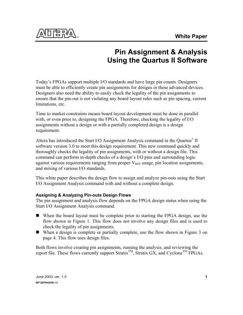
Pin Assignment & Analysis Using the Quartus II Software
Pin Assignment & Analysis Using the Quartus II Software
Pin Assignment & Analysis Using the Quartus II Software
Create successful ePaper yourself
Turn your PDF publications into a flip-book with our unique Google optimized e-Paper software.
White Paper<br />
<strong>Pin</strong> <strong>Assignment</strong> & <strong>Analysis</strong><br />
<strong>Using</strong> <strong>the</strong> <strong>Quartus</strong> <strong>II</strong> <strong>Software</strong><br />
Today’s FPGAs support multiple I/O standards and have large pin counts. Designers<br />
must be able to efficiently create pin assignments for designs in <strong>the</strong>se advanced devices.<br />
Designers also need <strong>the</strong> ability to easily check <strong>the</strong> legality of <strong>the</strong> pin assignments to<br />
ensure that <strong>the</strong> pin-out is not violating any board layout rules such as pin spacing, current<br />
limitations, etc.<br />
Time to market constraints means board layout development must be done in parallel<br />
with, or even prior to, designing <strong>the</strong> FPGA. Therefore, checking <strong>the</strong> legality of I/O<br />
assignments without a design or with a partially completed design is a design<br />
requirement.<br />
Altera has introduced <strong>the</strong> Start I/O <strong>Assignment</strong> <strong>Analysis</strong> command in <strong>the</strong> <strong>Quartus</strong> R <strong>II</strong><br />
software version 3.0 to meet this design requirement. This new command quickly and<br />
thoroughly checks <strong>the</strong> legality of pin assignments, with or without a design file. This<br />
command can perform in-depth checks of a design’s I/O pins and surrounding logic<br />
against various requirements ranging from proper VREF usage, pin location assignments,<br />
and mixing of various I/O standards.<br />
This white paper describes <strong>the</strong> design flow to assign and analyze pin-outs using <strong>the</strong> Start<br />
I/O <strong>Assignment</strong> <strong>Analysis</strong> command with and without a complete design.<br />
Assigning & Analyzing <strong>Pin</strong>-outs Design Flows<br />
The pin assignment and analysis flow depends on <strong>the</strong> FPGA design status when using <strong>the</strong><br />
Start I/O <strong>Assignment</strong> <strong>Analysis</strong> command.<br />
� When <strong>the</strong> board layout must be complete prior to starting <strong>the</strong> FPGA design, use <strong>the</strong><br />
flow shown in Figure 1. This flow does not involve any design files and is used to<br />
check <strong>the</strong> legality of pin assignments.<br />
� When a design is complete or partially complete, use <strong>the</strong> flow shown in Figure 3 on<br />
page 4. This flow uses design files.<br />
Both flows involve creating pin assignments, running <strong>the</strong> analysis, and reviewing <strong>the</strong><br />
report file. These flows currently support Stratix TM , Stratix GX, and Cyclone TM FPGAs.<br />
June 2003, ver. 1.0 1<br />
WP-Q<strong>II</strong>PNASGN-1.0
<strong>Pin</strong> <strong>Assignment</strong> & <strong>Analysis</strong> <strong>Using</strong> <strong>the</strong> <strong>Quartus</strong> <strong>II</strong> <strong>Software</strong> Altera Corporation<br />
Design Flow without Design Files<br />
During <strong>the</strong> early stages of development of an FPGA device, board layout engineers may<br />
request preliminary or final pin-outs. With <strong>the</strong> <strong>Assignment</strong> Editor, tool command<br />
langauge (Tcl) scripting, or by directly editing <strong>the</strong> <strong>the</strong> complier settings file (.csf),<br />
designers can create pin related assignments like locations and I/O standards for <strong>the</strong><br />
FPGA design. The Start I/O <strong>Assignment</strong> <strong>Analysis</strong> command checks on <strong>the</strong> legality of<br />
<strong>the</strong>se assignments.<br />
Figure 1. Assigning & Analyzing <strong>Pin</strong>-outs without Design Files<br />
2<br />
<strong>Quartus</strong> <strong>II</strong> project (.quartus)<br />
Create pin-related assignments<br />
.csf, .esf<br />
Start I/O assignment analysis<br />
Report file generated<br />
Modify and correct illegal<br />
assignments found in report file<br />
To assign and analyze pin-outs using <strong>the</strong> I/O <strong>Assignment</strong> <strong>Analysis</strong> command without<br />
design files:<br />
1. Create a <strong>Quartus</strong> <strong>II</strong> project and select <strong>the</strong> target device.<br />
2. Make pin assignments. Because <strong>the</strong>re are no design files, pin-related assignments<br />
(I/O standards, toggle rate, current strength, etc.) can be made to reserved pins<br />
using <strong>the</strong> <strong>Assignment</strong> Editor or with <strong>the</strong> Tcl scripting interface. See <strong>the</strong> Creating<br />
I/O <strong>Assignment</strong>s section of this document.<br />
3. Run <strong>the</strong> Start I/O <strong>Assignment</strong> <strong>Analysis</strong> command and view <strong>the</strong> report file.<br />
4. Correct any errors reported by <strong>the</strong> I/O assignment analysis and re-run <strong>the</strong><br />
analysis.
Altera Corporation <strong>Pin</strong> <strong>Assignment</strong> & <strong>Analysis</strong> <strong>Using</strong> <strong>the</strong> <strong>Quartus</strong> <strong>II</strong> <strong>Software</strong><br />
Design Flow with Design Files<br />
In this flow, run <strong>the</strong> Start I/O <strong>Assignment</strong> <strong>Analysis</strong> command before a full compilation.<br />
During a full compilation, illegal pin assignments are not found until <strong>the</strong> fitter stage of a<br />
compilation. Because <strong>the</strong> errors are reported during fitting, errors are not caught quickly.<br />
By running <strong>the</strong> Start I/O <strong>Assignment</strong> <strong>Analysis</strong> command before full compilation, any<br />
incorrect pin assignments are reported within minutes. The I/O assignment analysis takes<br />
on average less than one minute compared to compilation, which can take hours. Figure 2<br />
illustrates saving compilation time with <strong>the</strong> Start I/O <strong>Assignment</strong> <strong>Analysis</strong> command.<br />
Figure 2. Saving Compilation Time with <strong>the</strong> Start I/O <strong>Assignment</strong> <strong>Analysis</strong><br />
Command<br />
I/O<br />
assignment<br />
analysis<br />
Full compilation<br />
Error<br />
reported<br />
and fixed<br />
Full compilation<br />
Error reported and fixed<br />
Full compilation<br />
3
<strong>Pin</strong> <strong>Assignment</strong> & <strong>Analysis</strong> <strong>Using</strong> <strong>the</strong> <strong>Quartus</strong> <strong>II</strong> <strong>Software</strong> Altera Corporation<br />
Figure 3. Assigning & Analyzing <strong>Pin</strong>-outs with Design Files<br />
4<br />
<strong>Quartus</strong> <strong>II</strong> project (.quartus)<br />
Create pin-related assignments<br />
.csf, .esf<br />
<strong>Analysis</strong> and syn<strong>the</strong>sis<br />
Mapped netlist<br />
Start I/O assignment analysis<br />
Report file generated<br />
Back annotate I/O assignment<br />
analysis pin placements<br />
Design files .edf, .vqm, .v, .vhd, .bdf<br />
Modify and correct illegal<br />
assignments found in report file<br />
To assign and analyze pin-outs using <strong>the</strong> Start I/O <strong>Assignment</strong> <strong>Analysis</strong> command with<br />
design files:<br />
1. Create a <strong>Quartus</strong> <strong>II</strong> project and design files.<br />
2. Create pin-related assignments with <strong>the</strong> <strong>Assignment</strong> Editor or <strong>the</strong> Tcl interface. <strong>Pin</strong><br />
related assignments include I/O standards, toggle rate, current strength, termination<br />
type, etc. <strong>Pin</strong> location assignments can also be created by dragging and dropping pins<br />
from <strong>the</strong> node finder to <strong>the</strong> floorplan editor.<br />
3. Analyze and syn<strong>the</strong>size <strong>the</strong> design to generate <strong>the</strong> internal mapped netlist.
Altera Corporation <strong>Pin</strong> <strong>Assignment</strong> & <strong>Analysis</strong> <strong>Using</strong> <strong>the</strong> <strong>Quartus</strong> <strong>II</strong> <strong>Software</strong><br />
4. Run <strong>the</strong> Start I/O <strong>Assignment</strong> <strong>Analysis</strong> command. This command was designed to be<br />
used frequently. The time it takes to run is in <strong>the</strong> range of seconds and minutes.<br />
5. The analysis should be performed repeatedly until <strong>the</strong>re are no errors found.<br />
However, if <strong>the</strong>re are changes to <strong>the</strong> PLLs, LVDS blocks, gigabit transceiver blocks<br />
(GXBs), or pin assignments in <strong>the</strong> design, <strong>the</strong>n running this command before a full<br />
compilation is highly recommended.<br />
6. Correct and rerun <strong>the</strong> analysis after <strong>the</strong> errors have been identified in <strong>the</strong> generated<br />
analysis report. The report includes a pin-out file and a list of resource usage along<br />
with <strong>the</strong> errors.<br />
Inputs Used for I/O <strong>Assignment</strong> <strong>Analysis</strong><br />
I/O assignments are stored into settings files that are read into <strong>the</strong> Start I/O <strong>Assignment</strong><br />
<strong>Analysis</strong> command along with <strong>the</strong> mapped netlist, if <strong>the</strong> second flow is used.<br />
With <strong>Quartus</strong> <strong>II</strong> software version 3.0, <strong>the</strong>re are many ways to create pin-related<br />
assignments as well as new types of assignments like assigning pins to I/O banks device<br />
edges.<br />
Creating I/O <strong>Assignment</strong>s<br />
Creating I/O assignments can be cumbersome and may require a great deal of time from<br />
<strong>the</strong> designer. To satisfy designer preferences and help designers efficiently create <strong>the</strong>se<br />
assignments, Altera provides three methods for creating I/O pin assignments:<br />
� The <strong>Assignment</strong> Editor<br />
� Tcl scripts<br />
� Drag and drop capability for nodes from <strong>the</strong> node filter to <strong>the</strong> floorplan editor<br />
Types of I/O pin assignments include various I/O standards, current strengths, on-chip<br />
termination settings, timing constraints, etc.<br />
All pin related assignments are stored in <strong>the</strong> .csf or .esf file and are read into <strong>the</strong> Start I/O<br />
<strong>Assignment</strong> <strong>Analysis</strong> command.<br />
For more information on using <strong>the</strong> <strong>Assignment</strong> Editor with <strong>the</strong> <strong>Quartus</strong> <strong>II</strong> software, refer<br />
to <strong>the</strong> <strong>Using</strong> <strong>the</strong> <strong>Assignment</strong> Editor in <strong>the</strong> <strong>Quartus</strong> <strong>II</strong> <strong>Software</strong> white paper.<br />
5
<strong>Pin</strong> <strong>Assignment</strong> & <strong>Analysis</strong> <strong>Using</strong> <strong>the</strong> <strong>Quartus</strong> <strong>II</strong> <strong>Software</strong> Altera Corporation<br />
Location <strong>Assignment</strong>s<br />
A new feature in <strong>the</strong> <strong>Quartus</strong> <strong>II</strong> software version 3.0 is <strong>the</strong> ability to assign pins to banks<br />
and edges. Altera R devices have numerous I/O banks available, and it is common to see a<br />
group of pins (buses) with compatible I/O standards placed into a particular bank or<br />
banks.<br />
Edges of a chip can also be used as a placement location. For example, in Stratix devices,<br />
all differential high-speed I/O pins are located on <strong>the</strong> left and right edges of <strong>the</strong> device.<br />
Assigning pins to edges is ideal for making LVDS pin location assignments where exact<br />
pin location is flexible. Figure 4 shows <strong>the</strong> Altera device package edges.<br />
Figure 4. Package View of <strong>the</strong> Four Edges on an Altera Device<br />
6<br />
Top Edge<br />
Left Edge Right Edge<br />
Bottom Edge<br />
<strong>Assignment</strong>s with <strong>the</strong> Floorplan Editor<br />
Ano<strong>the</strong>r method of making pin assignments, in addition to <strong>the</strong> <strong>Assignment</strong> Editor and <strong>the</strong><br />
Tcl interface is through <strong>the</strong> Floorplan Editor. To access <strong>the</strong> Floorplan Editor Timing<br />
Closure Floorplan choose Timing Closure Floorplan (<strong>Assignment</strong>s menu).<br />
With <strong>the</strong> Timing Closure floorplan, <strong>the</strong> designer can toggle between <strong>the</strong> package view<br />
and <strong>the</strong> interior detailed view. In both views <strong>the</strong> designer can drag and drop pins from <strong>the</strong><br />
node finder or a block diagram file (.bdf) into a desired pin or bank in <strong>the</strong> Floorplan<br />
Editor. See Figure 5.<br />
The Floorplan Editor is a great way to create pin assignments as <strong>the</strong> designer can see<br />
where <strong>the</strong> pins will be located without having to reference <strong>the</strong> pin package<br />
documentation.
Altera Corporation <strong>Pin</strong> <strong>Assignment</strong> & <strong>Analysis</strong> <strong>Using</strong> <strong>the</strong> <strong>Quartus</strong> <strong>II</strong> <strong>Software</strong><br />
Figure 5. Creating <strong>Pin</strong> Location <strong>Assignment</strong>s with <strong>the</strong> Node Finder & <strong>the</strong> Timing<br />
Closure Floorplan Editor.<br />
Generating a Mapped Netlist<br />
A mapped netlist is only required in <strong>the</strong> flow shown in Figure 3 for saving compilation<br />
times with <strong>the</strong> Start I/O <strong>Assignment</strong> <strong>Analysis</strong> command. The internal netlist is used to<br />
identify what <strong>the</strong> pin names are and <strong>the</strong>ir direction (input, output, bidirectional) and is<br />
used during <strong>the</strong> I/O analysis to perform a thorough check.<br />
The mapped netlist can be generated by running <strong>the</strong> analysis and syn<strong>the</strong>sis command in<br />
<strong>the</strong> <strong>Quartus</strong> <strong>II</strong> software. <strong>Analysis</strong> and syn<strong>the</strong>sis can be executed from <strong>the</strong> <strong>Quartus</strong> <strong>II</strong> menu<br />
or with <strong>the</strong> quartus_map executable.<br />
The mapped netlist generated is stored internally in <strong>the</strong> <strong>Quartus</strong> <strong>II</strong> database (\db)<br />
directory.<br />
7
<strong>Pin</strong> <strong>Assignment</strong> & <strong>Analysis</strong> <strong>Using</strong> <strong>the</strong> <strong>Quartus</strong> <strong>II</strong> <strong>Software</strong> Altera Corporation<br />
Running <strong>the</strong> I/O <strong>Assignment</strong> <strong>Analysis</strong><br />
The Start I/O <strong>Assignment</strong> <strong>Analysis</strong> command runs legality checks on <strong>the</strong> user pin-outs,<br />
similar to <strong>the</strong> checks done in <strong>the</strong> fitter stage, as well as <strong>the</strong> surrounding logic which<br />
directly feeds or is fed by pins.<br />
The Start I/O <strong>Assignment</strong> <strong>Analysis</strong> command with <strong>the</strong> flow in Figure 3 can only perform<br />
simple checks, including placement and I/O standards, with <strong>the</strong> user pin-outs.<br />
The flow in Figure 3 suggests running <strong>the</strong> I/O assignment analysis any time a change is<br />
made to <strong>the</strong> pin assignments of <strong>the</strong> design before executing a full compilation. The<br />
analysis checks all <strong>the</strong> pin assignments and surrounding logic for illegal assignments,<br />
e.g., <strong>the</strong> pad spacing requirements between different I/O standards are violated. These<br />
checks may include if <strong>the</strong> pin location supports <strong>the</strong> I/O standard assigned, a legal current<br />
strength, supported VREF voltages, or if <strong>the</strong> PCI diode is allowed.<br />
Besides <strong>the</strong> I/O pins, <strong>the</strong> Start I/O <strong>Assignment</strong> <strong>Analysis</strong> command also checks blocks that<br />
directly feed or are fed by a pin such as PLLs, LVDS, and GXB blocks. For example, this<br />
command checks that <strong>the</strong> pin assignment for a PLL input can feed a PLL capable of<br />
operating at <strong>the</strong> specified frequency. In Stratix devices different PLLs and I/O banks have<br />
different capabilities, so it is important to select valid pins.<br />
The Start I/O <strong>Assignment</strong> <strong>Analysis</strong> command can be executed from <strong>the</strong> <strong>Quartus</strong> <strong>II</strong><br />
software menu (see Figure 6) or from <strong>the</strong> command prompt. Run <strong>the</strong> command by<br />
choosing Start > Start I/O <strong>Assignment</strong> <strong>Analysis</strong> (Processing menu).<br />
8
Altera Corporation <strong>Pin</strong> <strong>Assignment</strong> & <strong>Analysis</strong> <strong>Using</strong> <strong>the</strong> <strong>Quartus</strong> <strong>II</strong> <strong>Software</strong><br />
Figure 6. Running <strong>the</strong> I/O <strong>Assignment</strong> <strong>Analysis</strong> Command from <strong>the</strong> <strong>Quartus</strong> <strong>II</strong><br />
<strong>Software</strong> Menu<br />
To run <strong>the</strong> Start I/O <strong>Assignment</strong> <strong>Analysis</strong> command from a command prompt type in <strong>the</strong><br />
followiing text and press Enter:<br />
quartus_fit --check_ios<br />
When running this command, <strong>the</strong> fitter’s previous compilation results are overwritten.<br />
Any o<strong>the</strong>r results, such as analysis and syn<strong>the</strong>sis or timing analysis, are not affected.<br />
Understanding <strong>the</strong> I/O <strong>Assignment</strong> <strong>Analysis</strong> Report<br />
The report file generated from runnng <strong>the</strong> Start I/O <strong>Assignment</strong> <strong>Analysis</strong> command<br />
provides a detailed summary of <strong>the</strong> I/O assignments in <strong>the</strong> project. The report file follows<br />
<strong>the</strong> format similar to <strong>the</strong> compilation report. See Figure 7.<br />
In <strong>the</strong> resource section, a summary of all <strong>the</strong> input, output, and bidirectional pins and<br />
<strong>the</strong>ir placement are available. There is also a floorplan view for reference.<br />
9
<strong>Pin</strong> <strong>Assignment</strong> & <strong>Analysis</strong> <strong>Using</strong> <strong>the</strong> <strong>Quartus</strong> <strong>II</strong> <strong>Software</strong> Altera Corporation<br />
Figure 7. Summary of <strong>the</strong> I/O Bank Usage in <strong>the</strong> I/O <strong>Assignment</strong> <strong>Analysis</strong> Report<br />
Suggested & Partial Placement<br />
Along with <strong>the</strong> design’s fixed I/O assignments, <strong>the</strong>re may be I/O pins that <strong>the</strong> designer<br />
has not assigned to a particular pin.<br />
For example, a designer may run <strong>the</strong> I/O assignment analysis with a group of LVDS pins<br />
assigned to an edge (left or right for high-speed differential I/Os). The I/O assignment<br />
analysis performs <strong>the</strong> legality checks and also provide a suggested pin placement for <strong>the</strong><br />
LVDS pins within <strong>the</strong> edge.<br />
The suggested placement made by <strong>the</strong> analysis can <strong>the</strong>n be reviewed in <strong>the</strong> pin-out file<br />
and in <strong>the</strong> resource section of <strong>the</strong> report file.<br />
To accept <strong>the</strong> suggested pin locations from <strong>the</strong> I/O assignment analysis, <strong>the</strong> designer can<br />
use <strong>the</strong> back annotation option. The back annotation feature saves pin and device<br />
assignments into <strong>the</strong> settings file that can be viewed later with <strong>the</strong> <strong>Assignment</strong> Editor.<br />
Detailed Error/Status Messages<br />
One of <strong>the</strong> key features about <strong>the</strong> report file are <strong>the</strong> detailed messages. Incorrect I/O<br />
assignment errors have detailed messages indicating <strong>the</strong> node in question as well as a<br />
description of <strong>the</strong> problem. These detailed messages help <strong>the</strong> designer locate and fix <strong>the</strong><br />
reported problem.<br />
10
Altera Corporation <strong>Pin</strong> <strong>Assignment</strong> & <strong>Analysis</strong> <strong>Using</strong> <strong>the</strong> <strong>Quartus</strong> <strong>II</strong> <strong>Software</strong><br />
The designer can highlight <strong>the</strong> message and use <strong>the</strong> right mouse button to select Message<br />
Locations to locate <strong>the</strong> node in <strong>the</strong> <strong>Assignment</strong> Editor, source file, compilation report or<br />
<strong>the</strong> timing closure floorplan to help understand and resolve <strong>the</strong> problem.<br />
The messages displayed by <strong>the</strong> I/O assignment analysis are much more detailed than <strong>the</strong><br />
fitter messages in earlier versions of <strong>the</strong> <strong>Quartus</strong> <strong>II</strong> software. The detailed messages can<br />
be found in <strong>the</strong> Fitter Message section of <strong>the</strong> report file as well as <strong>the</strong> Processing tab in<br />
<strong>the</strong> messages window by choosing Utility Windows->Messages (View menu).<br />
Figure 8 is an example of an error message that <strong>the</strong> I/O assignment analysis reports.<br />
Figure 8. Example of Error Messages Reported by I/O <strong>Assignment</strong> <strong>Analysis</strong><br />
Conclusion<br />
The <strong>Quartus</strong> <strong>II</strong> software version 3.0 provides designers with <strong>the</strong> capabilities to efficiently<br />
create pin assignments and to quickly and thoroughly validate <strong>the</strong> legality of <strong>the</strong><br />
assignments. These capabilities can help reduce development time by catching illegal pin<br />
and surrounding logic assignments early in <strong>the</strong> design cycle without long design<br />
compilations.<br />
By providing <strong>the</strong> designer with more confidence in <strong>the</strong> current design pin-outs, board<br />
layout engineers can work in parallel with FPGA designers to provide a shorter time-to<br />
market for <strong>the</strong>ir product.<br />
11
<strong>Pin</strong> <strong>Assignment</strong> & <strong>Analysis</strong> <strong>Using</strong> <strong>the</strong> <strong>Quartus</strong> <strong>II</strong> <strong>Software</strong> Altera Corporation<br />
101 Innovation Drive<br />
San Jose, CA 95134<br />
(408) 544-7000<br />
www.altera.com<br />
12<br />
Copyright © 2003 Altera Corporation. All rights reserved. Altera, The Programmable Solutions<br />
Company, <strong>the</strong> stylized Altera logo, specific device designations, and all o<strong>the</strong>r words and logos<br />
that are identified as trademarks and/or service marks are, unless noted o<strong>the</strong>rwise, <strong>the</strong><br />
trademarks and service marks of Altera Corporation in <strong>the</strong> U.S. and o<strong>the</strong>r countries.* All o<strong>the</strong>r<br />
product or service names are <strong>the</strong> property of <strong>the</strong>ir respective holders. Altera products are<br />
protected under numerous U.S. and foreign patents and pending applications, maskwork<br />
rights, and copyrights. Altera warrants performance of its semiconductor products to current<br />
specifications in accordance with Altera’s standard warranty, but reserves <strong>the</strong> right to make<br />
changes to any products and services at any time without notice. Altera assumes no<br />
responsibility or liability arising out of <strong>the</strong> application or use of any information, product, or<br />
service described herein except as expressly agreed to in writing by Altera Corporation. Altera<br />
customers are advised to obtain <strong>the</strong> latest version of device specifications before relying on<br />
any published information and before placing orders for products or services.


