A Full-Featured Wireless Interface for RS-232 Communications
A Full-Featured Wireless Interface for RS-232 Communications
A Full-Featured Wireless Interface for RS-232 Communications

Create successful ePaper yourself
Turn your PDF publications into a flip-book with our unique Google optimized e-Paper software.
Paul Sofianos<br />
Motorola, Inc., WSSG RF/IF Applications Engineering<br />
Freescale Semiconductor, Inc.<br />
Order this document by AN1687/D<br />
<br />
nc...<br />
Freescale Semiconductor, I<br />
INTRODUCTION<br />
This application note describes a full–duplex, wireless<br />
data communication link targeted <strong>for</strong> <strong>RS</strong>–<strong>232</strong> applications.<br />
An encoding technique has been designed which addresses<br />
many of the problems incurred when attempting to implement<br />
the <strong>RS</strong>–<strong>232</strong> (EIA–<strong>232</strong>) standard, including but not limited to:<br />
hardware flow control, the DC component of the transmitted<br />
signal, automatic synchronization from host to slave and<br />
error detection. The design emulates a <strong>RS</strong>–<strong>232</strong> null modem<br />
cable <strong>for</strong> computer–to–computer communications.<br />
The actual design was realized with standard SSI logic<br />
from the high speed CMOS family (MC74HCxxx), an HC05<br />
based MCU, and Motorola’s ISM Band RF chipset. The<br />
targeted data rate was 57,600 Baud, although both higher<br />
and lower data rates are easily attainable. It is expected that<br />
most applications would embed the logic functions (and<br />
possibly the MCU functions) into a FPGA, CPLD, ASIC, or<br />
other LSI logic building block.<br />
Throughout this application note, it is assumed the user is<br />
familiar with standard TTL–compatible CMOS devices and<br />
the ISM Band RF chipset. Please refer to DL110/D and<br />
DL129/D <strong>for</strong> additional details on individual device<br />
specifications.<br />
THE WIRELESS LINK<br />
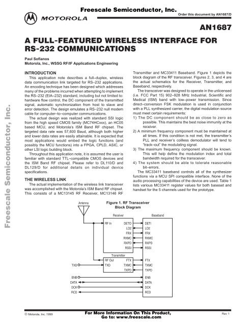
The actual implementation of the wireless link transceiver<br />
was accomplished with the Motorola’s ISM Band RF chipset.<br />
This consists of a MC13145 RF Receiver, MC13146 RF<br />
Antenna<br />
Figure 1. RF Transceiver<br />
Block Diagram<br />
RF In<br />
Receiver<br />
DETO<br />
LO2<br />
FRX<br />
RXMC<br />
RXPD<br />
<strong>RS</strong>SI<br />
Transmitter and MC33411 Baseband. Figure 1 depicts the<br />
block diagram of the RF transceiver. Figures 2, 3, and 4 are<br />
the actual schematics <strong>for</strong> the Receiver, Transmitter, and<br />
Baseband, respectively.<br />
The transceiver was designed to operate in the unlicensed<br />
(i.e. FCC Part 15) 902–928 MHz Industrial, Scientific and<br />
Medical (ISM) band with low–power transmission. Since<br />
direct–conversion FSK modulation is used in conjunction<br />
with a PLL synthesized carrier, the digital modulation source<br />
must meet certain requirements:<br />
1) The DC component should be as close to zero as<br />
possible. This maintains the best noise immunity at the<br />
receiver.<br />
2) A minimum frequency component must be maintained at<br />
all times. If this condition is not met, the transmitter’s<br />
PLL and receiver’s coilless demodulator will tend to<br />
“track–out” the modulating signal.<br />
3) The maximum frequency component should be known.<br />
This will help define the modulation index and total<br />
bandwidth required <strong>for</strong> the transceiver.<br />
4) The system should be able to tolerate reasonable<br />
bit–errors.<br />
The MC33411 baseband controls all of the synthesizer<br />
functions via a MCU SPI compatible interface. None of the<br />
audio processing capabilities of the device are used. Table 1<br />
lists various MC33411 register values <strong>for</strong> both baseset and<br />
handset <strong>for</strong> the 5 channels used <strong>for</strong> the prototype.<br />
DETI<br />
LO2<br />
FRX<br />
RXMC<br />
RXPD<br />
<strong>RS</strong>SI<br />
Baseband<br />
TXD<br />
ENB<br />
DATA<br />
DCK<br />
RCD<br />
Transmitter<br />
RF Out FTX<br />
TXD TXMC<br />
TXPD<br />
FTX<br />
TXMC<br />
TXPD<br />
ENB<br />
DATA<br />
DCK<br />
RCD<br />
© MOTOROLA Motorola, Inc. 1999 For More In<strong>for</strong>mation On This Product,<br />
Rev<br />
RF/IF APPLICATIONS INFORMATION<br />
11<br />
Go to: www.freescale.com
Freescale Semiconductor, Inc.<br />
Figure 2. RF Receiver<br />
VCC<br />
C7 100 p<br />
C8 1.0 n<br />
R2 300<br />
nc...<br />
Freescale Semiconductor, I<br />
RF In<br />
RXPD<br />
LO2<br />
RXMC<br />
C37<br />
100 p<br />
R9<br />
33 k<br />
CF4<br />
C10<br />
CF3<br />
C35 1.0 n<br />
C34 100 p<br />
C6 100 p L5<br />
6.8 n<br />
100 p<br />
VCC<br />
C11<br />
4.7 p<br />
D1<br />
C12<br />
L6<br />
4.7 p<br />
2.2 n<br />
C36 100 p<br />
C41<br />
C30<br />
0.01<br />
1.0 n<br />
C31 1.0 n<br />
R4 100 k<br />
R5 2.85 k<br />
R6<br />
C32<br />
120 k<br />
1.0<br />
VCC<br />
14<br />
19<br />
22<br />
23<br />
24<br />
30<br />
33<br />
20<br />
29<br />
47<br />
2<br />
3<br />
4<br />
21<br />
10<br />
LNA In<br />
Mix1 In<br />
oscC<br />
oscE<br />
oscB<br />
Mix2 In<br />
LO2<br />
Lin Adj1<br />
Lin Adj2<br />
BWadj<br />
Fadj<br />
AFT Out<br />
AFT In<br />
EN<br />
MC<br />
U1<br />
LNA Out<br />
IF1+<br />
IF1–<br />
IF2+<br />
17<br />
27<br />
28<br />
35<br />
IF2–<br />
36<br />
IF Dec1<br />
39<br />
IF Dec2<br />
IF In<br />
IF Out<br />
Lim Dec1<br />
40<br />
38<br />
41<br />
45<br />
Lim Dec2<br />
46<br />
Lim In<br />
44<br />
Det G<br />
5<br />
Det Out<br />
6<br />
<strong>RS</strong>SI<br />
7<br />
PRES Out<br />
9<br />
C13<br />
16 p<br />
C45 +<br />
1.0<br />
C15 36 p<br />
C28 0.1<br />
C22 0.1<br />
C9 100 p<br />
C26 0.01<br />
C39 100 p<br />
C16<br />
C18 1.0 n<br />
C19 1.0 n<br />
C20 1.0 n<br />
C21 1.0 n<br />
C46 1.0 n<br />
C50 100 p<br />
R3<br />
C25<br />
R11<br />
39 p<br />
27 k<br />
47 p<br />
L7 2.7<br />
L8 2.7<br />
33 k<br />
CF2 CF1<br />
R10<br />
10<br />
T1<br />
C47 1.0 n<br />
C51 100 p<br />
C14<br />
VCC<br />
10 p<br />
C48 1.0 n<br />
C40<br />
12 p<br />
C52 100 p<br />
VCC<br />
VCC<br />
C42 100 p<br />
C27 0.01<br />
C17 1.0 n<br />
C29 0.1<br />
C23 1.0 n<br />
C24 0.1<br />
C49 1.0 n<br />
C53 100 p<br />
VCC<br />
VCC<br />
DETO<br />
<strong>RS</strong>SI<br />
Default Units: Ohms, Microfarads and Microhenries<br />
CF1,CF2 Toko Type CFSK Series<br />
SK107MX–AE–XXX, 330 kHz BW<br />
CF3,CF4 Handset: TDK CF6118702<br />
Baseset: TDK CF6118902<br />
D1 MMBV809LT1<br />
T1 Toko A638AN–A099YWN<br />
MC13145<br />
C43 22 n<br />
C44 0.01<br />
FRX<br />
2 For More In<strong>for</strong>mation On This<br />
MOTOROLA<br />
Product,<br />
RF/IF APPLICATIONS INFORMATION<br />
Go to: www.freescale.com
Freescale Semiconductor, Inc.<br />
<br />
TXPD<br />
Figure 3. RF Transmitter<br />
VCC<br />
nc...<br />
Freescale Semiconductor, I<br />
TXD<br />
Appx.<br />
1.5 VPP<br />
TXMC<br />
R20<br />
10 k<br />
C77<br />
47 p<br />
D3<br />
C78<br />
47 p<br />
C75<br />
0.5 p<br />
R19<br />
10 k<br />
C74<br />
15 p<br />
C68<br />
100 p<br />
Default Units: Ohms, Microfarads and Microhenries<br />
CF5 Handset: TDK CF 6118902<br />
Baseset: TDK CF 6118702<br />
D2,D3 MMBV809LT1<br />
D2<br />
C65<br />
47 p<br />
L10<br />
1.8 n<br />
C66<br />
100 p<br />
C67<br />
1.0 n<br />
VCC<br />
R13<br />
150<br />
C54<br />
1.0 n<br />
L9<br />
10 n<br />
VCC<br />
9<br />
C63<br />
2.7 p<br />
11<br />
C64<br />
2.7 p<br />
12<br />
5<br />
4<br />
22<br />
16<br />
17<br />
MC13146<br />
OSCB<br />
OSCE<br />
OSCC<br />
MIX/BUF_IN<br />
LINADJ<br />
PA_IN<br />
MC<br />
EN<br />
U2<br />
RF–<br />
RF+<br />
PA_OUT<br />
P<strong>RS</strong>COUT<br />
R22<br />
51<br />
1<br />
3<br />
19<br />
14<br />
C56<br />
1.0<br />
VCC<br />
R14<br />
200<br />
C70<br />
0.01<br />
+<br />
C57<br />
1.0 n<br />
C72<br />
C60<br />
100 p<br />
C71<br />
100 p<br />
100 p<br />
C58<br />
1.0 n<br />
C61<br />
100 p<br />
CF5<br />
C59<br />
1.0 n<br />
C62<br />
100 p<br />
C55<br />
1.0 n<br />
FTX<br />
VCC<br />
RF Out<br />
For More In<strong>for</strong>mation On This Product,<br />
MOTOROLA RF/IF APPLICATIONS INFORMATION<br />
Go to: www.freescale.com<br />
3
Freescale Semiconductor, Inc.<br />
Figure 4. Baseband<br />
C94<br />
4.7<br />
C114<br />
100 p<br />
VCCA<br />
C95<br />
0.1<br />
VCC<br />
R31<br />
10<br />
C97<br />
1.0<br />
VCCA<br />
C96<br />
1.0 n<br />
nc...<br />
Freescale Semiconductor, I<br />
<strong>RS</strong>SI<br />
DETI<br />
LO2<br />
RXMC<br />
FRX<br />
RXPD<br />
C93<br />
L12<br />
150 n<br />
C104<br />
R28<br />
100 p<br />
82 p<br />
68 k<br />
R35<br />
18 k<br />
C107 1.0<br />
C92<br />
27 p<br />
R29<br />
C105<br />
C91<br />
VCC<br />
270 k<br />
3.9 n<br />
470 p<br />
VCC<br />
R30<br />
51<br />
Default Units: Ohms, Microfarads and Microhenries<br />
37<br />
38<br />
39<br />
40<br />
41<br />
42<br />
43<br />
44<br />
45<br />
46<br />
47<br />
48<br />
<strong>RS</strong>SI In<br />
Rx Audio In<br />
DS In<br />
Gnd Audio<br />
LO2 Out<br />
LO2 VCC<br />
LO2+<br />
LO2 Ctl<br />
LO2–<br />
LO2 Gnd<br />
LO2 PD<br />
LO2 Gnd<br />
VCCR<br />
R x<br />
O ut<br />
3<br />
6<br />
F<br />
R x<br />
M<br />
C<br />
C90 2.7 n<br />
C89 0.01 R27<br />
C88 200 p R26<br />
E<br />
I<br />
n<br />
3<br />
5 3 4<br />
E<br />
c<br />
a<br />
p<br />
3<br />
3<br />
2<br />
3<br />
1<br />
3<br />
0<br />
2<br />
9<br />
2<br />
8<br />
2<br />
7<br />
2<br />
6<br />
3<br />
E P G P P V V<br />
O AI nd AO– AO+ CC B<br />
ut<br />
S S<br />
A A<br />
V AG<br />
M CI<br />
U3<br />
MC33411<br />
P P P LL LL LL F<br />
R T Tx<br />
F V x<br />
G x D<br />
V F C ata<br />
R CC P nd P CC Tx M E LK x D D C N<br />
2<br />
5<br />
1 2 3 4 5 6 7 8 9 1 0<br />
1 1<br />
1 2<br />
180 k<br />
51 k<br />
R24<br />
R25<br />
MCO<br />
VCC Audio<br />
C In<br />
Ccap<br />
C Out<br />
Lim In<br />
Tx Out<br />
DS Out<br />
Fref Out<br />
Fref In<br />
Gnd Digital<br />
MCU Clk Out<br />
C85 0.33<br />
20 k C86 1.0<br />
2.0 k C87 0.1<br />
24<br />
23<br />
22<br />
21<br />
20<br />
19<br />
18<br />
17<br />
16<br />
15<br />
14<br />
13<br />
VCCA<br />
C113<br />
100 p<br />
C83<br />
Y1<br />
11.2 M<br />
C84<br />
5–40 p<br />
20 p<br />
R32<br />
10<br />
C111<br />
1.0<br />
C112<br />
1.0<br />
RCD<br />
DATA<br />
DCK<br />
ENB<br />
TXMC<br />
FTX<br />
TXPD<br />
VCCR<br />
C98<br />
1.0 n<br />
C99<br />
1.0 n<br />
4 For More In<strong>for</strong>mation On This<br />
MOTOROLA<br />
Product,<br />
RF/IF APPLICATIONS INFORMATION<br />
Go to: www.freescale.com
DIGITAL ENCODING DESCRIPTION<br />
As mentioned above, it is necessary to encode the raw<br />
<strong>RS</strong>–<strong>232</strong> data prior to RF transmission since the incoming<br />
data stream can, and usually will, contain a DC component<br />
Freescale Semiconductor, Inc.<br />
<br />
and has no pre–defined minimum frequency component.<br />
Figure 5 is a block diagram of the digital encoder/decoder<br />
section, and Figure 6 shows a possible implementation of the<br />
encoder.<br />
Figure 5. Encoder/Decoder Block Diagram<br />
(Baseset Shown)<br />
nc...<br />
Freescale Semiconductor, I<br />
DB25<br />
P2<br />
1<br />
14<br />
2<br />
15<br />
3<br />
16<br />
4<br />
17<br />
5<br />
18<br />
6<br />
19<br />
7<br />
20<br />
8<br />
21<br />
9<br />
22<br />
10<br />
23<br />
11<br />
24<br />
12<br />
25<br />
13<br />
ETXD<br />
ERXD<br />
ERTS<br />
ECTS<br />
Translator<br />
TXD<br />
RXD<br />
RTS<br />
CTS<br />
To RF<br />
Transceiver<br />
Baseband<br />
TXD<br />
RXD<br />
RTS<br />
CTS<br />
DCK<br />
ENB<br />
DATA<br />
MCU<br />
D(0–7)<br />
I<br />
D/C<br />
NTXA<br />
TXR<br />
CK<br />
NRXA<br />
RXR<br />
FE<br />
16XCK<br />
D(0–7)<br />
I<br />
D/C<br />
NTXA<br />
TXR<br />
CK<br />
DETI<br />
I<br />
D/C<br />
NRXA<br />
RXR<br />
FE<br />
CK<br />
Parallel–Serial/<br />
Encoder<br />
DOUT<br />
Serial–Parallel/<br />
Decoder<br />
DIN<br />
TXD<br />
RCD<br />
For More In<strong>for</strong>mation On This Product,<br />
MOTOROLA RF/IF APPLICATIONS INFORMATION<br />
Go to: www.freescale.com<br />
5
Freescale Semiconductor, Inc.<br />
Figure 6. Encoder<br />
U1<br />
D/C<br />
9<br />
U5D<br />
8<br />
74HC04A<br />
V CC<br />
D7<br />
D6<br />
14<br />
15<br />
1<br />
2<br />
3<br />
4<br />
5<br />
6<br />
7<br />
SER<br />
A<br />
B<br />
C<br />
D<br />
E<br />
F<br />
G<br />
H<br />
QH 9<br />
CK<br />
NTXA<br />
CK<br />
CK<br />
11<br />
13<br />
10<br />
12<br />
SRCLK<br />
SRLOAD<br />
SRCLR<br />
RCLK<br />
74HC597A<br />
nc...<br />
Freescale Semiconductor, I<br />
D(0–7)<br />
I<br />
V CC<br />
V CC<br />
11<br />
CK<br />
U5E<br />
10<br />
74HC04A<br />
3<br />
4<br />
5<br />
6<br />
7<br />
10<br />
2<br />
9<br />
1<br />
A<br />
B<br />
C<br />
D<br />
ENP<br />
ENT<br />
CLK<br />
LOAD<br />
CLR<br />
U3<br />
D5<br />
D4<br />
D3<br />
D2<br />
D1<br />
D0<br />
QA<br />
QB<br />
QC<br />
QD<br />
RCO<br />
14<br />
13<br />
12<br />
11<br />
15<br />
14<br />
15<br />
1<br />
2<br />
3<br />
4<br />
5<br />
6<br />
7<br />
11<br />
13<br />
10<br />
12<br />
U24C<br />
8<br />
74HC32A<br />
SER<br />
A<br />
B<br />
C<br />
D<br />
E<br />
F<br />
G<br />
H<br />
SRCLK<br />
SRLOAD<br />
SRCLR<br />
RCLK<br />
10<br />
9<br />
74HC04A<br />
U2<br />
74HC597A<br />
U5F<br />
13 12<br />
QH 9<br />
11<br />
U15D<br />
74HC86A<br />
13<br />
12<br />
5 k<br />
C17<br />
C23<br />
R13<br />
U24D<br />
11<br />
74HC32A<br />
2200 p<br />
4700 p<br />
13<br />
12<br />
V CC<br />
U4B<br />
74HC109 11<br />
14 PR 10<br />
J<br />
Q<br />
CK<br />
12<br />
CLK<br />
13<br />
9<br />
K<br />
Q<br />
CL<br />
15<br />
DOUT<br />
TXR<br />
74HC163A<br />
Figure 7 illustrates the encoding scheme which was<br />
developed <strong>for</strong> this purpose. Four additional bits surround a<br />
data byte: the I bit, I bit, D/C bit and D/C bit. The function of<br />
these bits are:<br />
I (Invert) Bit: A logic low on this bit indicates that the data<br />
byte and D/C bit are in true <strong>for</strong>m. A logic high on this bit<br />
indicates that the data byte and D/C bit are complemented<br />
from their original <strong>for</strong>m.<br />
I (Invert Bar) Bit: Just the complement of the I bit.<br />
D/C (Data/Control) Bit: A logic low on this bit indicates<br />
that the data byte should be interpreted as a control word. A<br />
logic high on this bit indicates that the data byte contains real<br />
data.<br />
D/C (Data/Control): Just the complement of the D/C bit.<br />
Figure 7.<br />
D/C I I D0 D1 D2 D3 D4 D5 D6 D7 D/C D/C I<br />
6 For More In<strong>for</strong>mation On This<br />
MOTOROLA<br />
Product,<br />
RF/IF APPLICATIONS INFORMATION<br />
Go to: www.freescale.com
nc...<br />
Freescale Semiconductor, I<br />
This encoding scheme allows <strong>for</strong> the representation of 256<br />
unique data words and 256 unique control words. The control<br />
byte $h00 is reserved and referred to as the idle byte.<br />
When the Parallel–Input/Serial–Output (PISO) register is<br />
ready to transmit a data byte (TXR asserted), a check is<br />
made to see if real data has been transferred into the Serial<br />
<strong>Communications</strong> <strong>Interface</strong> (SCI) data register of the MCU. If<br />
data has been received, the data byte will be read, and the<br />
initial state of D/C will be set to 1. If data has not been<br />
received, the data byte will be set to $h00 (the idle byte) and<br />
the initial state of D/C will be set to 0.<br />
Next, the data byte is examined <strong>for</strong> a DC component. Each<br />
0 bit of the data byte represents –1 and each 1 bit of the data<br />
byte represents +1. All of these values are summed together:<br />
a negative result indicates a low DC component, zero<br />
indicates no DC component, and a positive (non–zero) result<br />
indicates a high DC component. This component is<br />
compared to a cumulative sum (which may be negative, zero,<br />
or positive) and the following actions are taken:<br />
If the current DC component sum is negative, and the<br />
cumulative sum is positive or zero<br />
OR<br />
if the current DC component sum is positive or zero and the<br />
cumulative sum is negative<br />
THEN<br />
clear the I bit (I=0). The new cumulative sum is equal to the<br />
old cumulative sum plus the current sum.<br />
OTHERWISE<br />
set the I bit (I=1). The new cumulative sum is equal to the old<br />
cumulative sum minus the current sum.<br />
If the I bit is set, the contents of the data byte and D/C bit<br />
are complemented.<br />
The updated value of the I bit, data byte, and D/C bit are<br />
placed on the PISO, and a transmission acknowledge signal<br />
(NTXA) is asserted. Please note, the net effect of the DC<br />
component contributed by the I and I bits and D/C and D/C<br />
bits will always equal zero.<br />
An analysis of this encoding scheme brings to light a few<br />
interesting observations:<br />
1) The average DC component over time will approach zero.<br />
2) The minimum frequency component which will be<br />
observed in the data stream will equal 1/(2 x<br />
transmitted bit period x 10).<br />
Freescale Semiconductor, Inc.<br />
<br />
3) The maximum (fundamental) frequency component which<br />
will be observed in the data stream will equal 1/(2 x<br />
transmitted bit period).<br />
4) A sequence of ten consecutive zeros or ones indicates the<br />
presence of an idle byte.<br />
Item 4 is perhaps the most interesting observation, since it<br />
will allow the receiver to synchronize the incoming data and<br />
align the serial stream on a byte–wide basis.<br />
TRANSMITTING FREQUENCY <strong>for</strong> ENCODED DATA<br />
For <strong>RS</strong>–<strong>232</strong> communications which take the <strong>for</strong>m of one<br />
start bit, eight data bits, no parity, and one stop bit, the SCI<br />
will receive 10 bits of data to represent one actual data byte.<br />
For our encoding scheme, 12 bits must be transmitted <strong>for</strong><br />
each data or control byte received. If the transmit pipeline is<br />
set to a frequency of at least 1.2 times the SCI receive<br />
pipeline, the receive bandwidth will not have to be reduced<br />
(i.e. no stop or hold conditions would be required).<br />
In actual practice, the transmit pipeline was set to a<br />
frequency 25% greater than the receive pipeline. As a result,<br />
at a minimum, there will be at least one idle byte transmitted<br />
<strong>for</strong> every 24 real data bytes. This useful feature allows the<br />
receiver to re–synchronize from time to time.<br />
ADDITIONAL FEATURES<br />
As mentioned above, the opportunity presents itself to<br />
transmit a control word (the idle byte just being a special case<br />
of a control word) from time to time. With 255 control words<br />
remaining, various special features can be built into the link,<br />
all transparent to the actual <strong>RS</strong>–<strong>232</strong> data communications.<br />
One of the more obvious features which can be<br />
implemented is hardware (RTS/CTS) flow control. The RTS<br />
signal (<strong>for</strong> the baseset) and CTS signal (<strong>for</strong> the handset) can<br />
be monitored and transmitted/received and interpreted by the<br />
link. The latency will mostly be a function of the overhead<br />
bandwidth.<br />
Other features which can be implemented include, but are<br />
not limited to:<br />
Remote channel changing<br />
Adaptive channel selection<br />
Acknowledgments<br />
DCD/DSR, etc. commands<br />
CRC or other error checking<br />
Half duplex handshaking<br />
Power conservation modes<br />
For More In<strong>for</strong>mation On This Product,<br />
MOTOROLA RF/IF APPLICATIONS INFORMATION<br />
Go to: www.freescale.com<br />
7
Freescale Semiconductor, Inc.<br />
Figure 8. Decoder<br />
V CC<br />
U16<br />
DIN<br />
16XCK<br />
16XCK<br />
V CC<br />
U14A<br />
74HC109 5<br />
2 PR 6<br />
J<br />
Q<br />
4<br />
CLK<br />
3<br />
7<br />
K<br />
Q<br />
CL<br />
1<br />
16XCK<br />
U14B<br />
74HC109 11<br />
14 PR 10<br />
J<br />
Q<br />
12<br />
CLK<br />
13<br />
9<br />
K<br />
Q<br />
CL<br />
15<br />
1<br />
U15A<br />
2<br />
74HC86A<br />
16XCK<br />
3<br />
V CC<br />
3<br />
4<br />
5<br />
6<br />
7<br />
10<br />
A<br />
B<br />
C<br />
D<br />
ENP<br />
ENT<br />
2<br />
CLK<br />
9<br />
LOAD<br />
1<br />
CLR<br />
74HC163A<br />
QA<br />
QB<br />
QC<br />
14<br />
13<br />
12<br />
11<br />
QD<br />
15<br />
RCO<br />
RCLK<br />
(Recovered CK)<br />
nc...<br />
Freescale Semiconductor, I<br />
1<br />
RDAT<br />
(Recovered Data)<br />
RCLK<br />
V CC<br />
RCLK<br />
V CC<br />
3<br />
4<br />
5<br />
6<br />
7<br />
10<br />
2<br />
9<br />
1<br />
A<br />
B<br />
C<br />
D<br />
ENP<br />
ENT<br />
CLK<br />
LOAD<br />
CLR<br />
V CC<br />
U17A<br />
74HC109 5<br />
2 PR 6<br />
J<br />
Q<br />
4<br />
CLK<br />
3<br />
7<br />
K<br />
Q<br />
CL<br />
1<br />
U21<br />
74HC163A<br />
QA<br />
QB<br />
QC<br />
14<br />
13<br />
12<br />
11<br />
QD<br />
15<br />
RCO<br />
V CC<br />
RCLK<br />
9<br />
1<br />
10<br />
2<br />
16XCK<br />
V CC<br />
U24A<br />
74HC32A<br />
U15C<br />
74HC86A<br />
3<br />
8<br />
V CC<br />
U17B<br />
74HC109 11<br />
14 PR 10<br />
J<br />
Q<br />
12<br />
CLK<br />
13<br />
9<br />
K<br />
Q<br />
CL<br />
15<br />
V CC<br />
U19A<br />
74HC109 5<br />
2 PR 6<br />
J<br />
Q<br />
4<br />
CLK<br />
3<br />
7<br />
K<br />
Q<br />
CL<br />
1<br />
4<br />
5<br />
U15B<br />
74HC86A<br />
RCLK<br />
6<br />
14<br />
RCLK 11<br />
V 10 CC<br />
12<br />
13<br />
V CC<br />
V CC<br />
SER<br />
SRCLK<br />
SRCLR<br />
RCLK<br />
G<br />
U20<br />
3<br />
4<br />
5<br />
6<br />
7<br />
10<br />
2<br />
9<br />
1<br />
74HC595A<br />
A<br />
B<br />
C<br />
D<br />
QA<br />
QB<br />
QC<br />
QD<br />
QE<br />
QF<br />
QG<br />
QH<br />
QH ′<br />
1<br />
4<br />
ENP<br />
ENT<br />
CLK<br />
LOAD<br />
CLR<br />
2<br />
5<br />
U18<br />
74HC163A<br />
15<br />
1<br />
2<br />
3<br />
4<br />
5<br />
6<br />
7<br />
9<br />
74HC86A<br />
U23B<br />
74HC86A<br />
QA<br />
QB<br />
QC<br />
14<br />
13<br />
12<br />
11<br />
QD<br />
15<br />
RCO<br />
6<br />
D7<br />
D6<br />
D5<br />
D4<br />
D3<br />
D2<br />
V CC<br />
U19B<br />
74HC109 11<br />
14 PR 10<br />
J<br />
Q<br />
12<br />
CLK<br />
13<br />
9<br />
K<br />
Q<br />
CL<br />
15<br />
14<br />
RCLK 11<br />
10<br />
V CC<br />
12<br />
13<br />
U23A<br />
9<br />
U23C<br />
V CC 8<br />
3<br />
10<br />
74HC86A<br />
12<br />
13<br />
U23D<br />
74HC86A<br />
SER<br />
SRCLK<br />
SRCLR<br />
RCLK<br />
G<br />
11<br />
U22<br />
D(0–7)<br />
74HC595A<br />
QA<br />
QB<br />
QC<br />
QD<br />
QE<br />
QF<br />
QG<br />
QH<br />
QH ′<br />
15<br />
1<br />
2<br />
3<br />
4<br />
5<br />
6<br />
7<br />
9<br />
D1<br />
D0<br />
4<br />
U24B<br />
6<br />
5<br />
74HC32A<br />
RXR<br />
D/C<br />
D(0–7)<br />
I<br />
NRXA<br />
FE<br />
8 For More In<strong>for</strong>mation On This<br />
MOTOROLA<br />
Product,<br />
RF/IF APPLICATIONS INFORMATION<br />
Go to: www.freescale.com
nc...<br />
Freescale Semiconductor, I<br />
Figure 8 illustrates a possible implementation of the digital<br />
decoder section of the design.<br />
Received data is “squared up” by the data slicer of the<br />
MC33411 baseband IC. The transmitted data is generally<br />
frequency limited in order to preserve bandwidth (i.e.<br />
low–pass filtered). Because of this limiting, as well as noise<br />
components and hysteresis in the data slicer, the duty cycle<br />
of the received data stream can vary substantially from that<br />
of the transmitted data. For this reason, a data and clock<br />
recovery block is utilized which oversamples the incoming<br />
data (digital noise filtering) and captures the embedded<br />
clock.<br />
Once the clock and data have been recovered, they are<br />
presented to the Serial–Input/Parallel–Output (SIPO)<br />
register. Data is transferred into the register every 12 bits,<br />
this representing the I, I, data byte, D/C and D/C bits. Another<br />
circuit analyzes the serial data stream looking <strong>for</strong> ten<br />
consecutive bits without a transition. If this condition is<br />
observed, it indicates an idle byte has been received, and the<br />
SIPO register clock can be synchronized.<br />
When the SIPO register indicates that a byte has been<br />
received (RXR asserted), the MCU asserts an<br />
acknowledgement (NRXA), loads the data byte, the I bit and<br />
D/C bit from the bus. At this time, a comparison is made<br />
which verifies that the I bit is the complement of the I bit and<br />
the D/C bit is the complement of the D/C bit. If either of these<br />
conditions is not met, a framing error has occurred and the<br />
received data is simply ignored.<br />
If a valid byte has been received, the MCU checks the<br />
status of the I bit. If the I bit is set, the byte, as well as the D/C<br />
Freescale Semiconductor, Inc.<br />
<br />
bit, is complemented. Next, the MCU checks the value of the<br />
updated D/C bit; a logic zero indicates a control word, and the<br />
MCU can take appropriate action.<br />
If the D/C bit indicates real data has been received, the<br />
data is placed on an internal First–In/First–Out (FIFO)<br />
memory stack. The SCI transmitter is checked: if empty, the<br />
next data byte is placed into the SCI transmitter and if full, the<br />
data will be transferred at a later time.<br />
As can be seen, the decoding of the data is a relatively<br />
simple task. If desired, the MCU can consider the lack of an<br />
idle byte, within a given period of time or reception of some<br />
number of bytes, an indication that the RF link has failed.<br />
Again, this condition can be used to re–initialize the RF link,<br />
or other courses of action can be taken.<br />
SUMMARY<br />
This application note has described a robust, full featured<br />
<strong>RS</strong>–<strong>232</strong> wireless interface which can be implemented with<br />
an inexpensive MCU. For slower data rates, it is possible to<br />
eliminate all of the external “glue logic” shown in this note. A<br />
plethora of additional features can be added by the use of<br />
embedded control words which are transparent to the actual<br />
data transceiver.<br />
Motorola’s inexpensive and easy to use ISM Band RF<br />
chipset is easily capable of accomplishing the wireless<br />
portion of the task as long as the digital in<strong>for</strong>mation presented<br />
to the transmitter and receiver have been properly<br />
preconditioned prior to modulation and demodulation.<br />
For More In<strong>for</strong>mation On This Product,<br />
MOTOROLA RF/IF APPLICATIONS INFORMATION<br />
Go to: www.freescale.com<br />
9
Freescale Semiconductor, Inc.<br />
Table 1.<br />
nc...<br />
Freescale Semiconductor, I<br />
Baseband<br />
Register<br />
Address<br />
Handset<br />
Value<br />
Transmit<br />
Frequency<br />
(MHz)<br />
Receive<br />
Frequency<br />
(MHz)<br />
Baseset<br />
Value<br />
Transmit<br />
Frequency<br />
(MHz)<br />
Receive<br />
Frequency<br />
(MHz)<br />
$h01 $h004822 925.0 – $h004686 903.0 – 0<br />
$h02 $h004C27 – 903.0 $h004E03 – 925.0 0<br />
$h01 $h004827 925.5 – $h00468B 903.5 – 1<br />
$h02 $h004C2C – 903.5 $h004E08 – 925.5 1<br />
$h01 $h00482C 926.0 – $h004690 904.0 – 2<br />
$h02 $h004C31 – 904.0 $h004E0D – 926.0 2<br />
$h01 $h004831 926.5 – $h004695 904.5 – 3<br />
$h02 $h004C36 – 904.5 $h004E12 – 926.5 3<br />
$h01 $h004836 927.0 – $h00469A 905.0 – 4<br />
$h02 $h004C3B – 905.0 $h004E17 – 927.0 4<br />
$h03 $h0E0276 – – $h0E0276 – – X<br />
$h04 $h160070 – – $h160070 – – X<br />
$h05 $h000010 – – $h000010 – – X<br />
$h06 $h0000FF – – $h0000FF – – X<br />
$h07 $h01C000 – – $h01C000 – – X<br />
Channel<br />
Number<br />
Motorola reserves the right to make changes without further notice to any products herein. Motorola makes no warranty, representation or guarantee regarding<br />
the suitability of its products <strong>for</strong> any particular purpose, nor does Motorola assume any liability arising out of the application or use of any product or circuit, and<br />
specifically disclaims any and all liability, including without limitation consequential or incidental damages. “Typical” parameters which may be provided in Motorola<br />
data sheets and/or specifications can and do vary in different applications and actual per<strong>for</strong>mance may vary over time. All operating parameters, including “Typicals”<br />
must be validated <strong>for</strong> each customer application by customer’s technical experts. Motorola does not convey any license under its patent rights nor the rights of<br />
others. Motorola products are not designed, intended, or authorized <strong>for</strong> use as components in systems intended <strong>for</strong> surgical implant into the body, or other<br />
applications intended to support or sustain life, or <strong>for</strong> any other application in which the failure of the Motorola product could create a situation where personal injury<br />
or death may occur. Should Buyer purchase or use Motorola products <strong>for</strong> any such unintended or unauthorized application, Buyer shall indemnify and hold Motorola<br />
and its officers, employees, subsidiaries, affiliates, and distributors harmless against all claims, costs, damages, and expenses, and reasonable attorney fees<br />
arising out of, directly or indirectly, any claim of personal injury or death associated with such unintended or unauthorized use, even if such claim alleges that<br />
Motorola was negligent regarding the design or manufacture of the part. Motorola and are registered trademarks of Motorola, Inc. Motorola, Inc. is an Equal<br />
Opportunity/Affirmative Action Employer.<br />
Mfax is a trademark of Motorola, Inc.<br />
How to reach us:<br />
USA / EUROPE / Locations Not Listed: Motorola Literature Distribution; JAPAN: Motorola Japan Ltd.; SPD, Strategic Planning Office, 141,<br />
P.O. Box 5405, Denver, Colorado 80217. 1–303–675–2140 or 1–800–441–2447 4–32–1 Nishi–Gotanda, Shinagawa–ku, Tokyo, Japan. 81–3–5487–8488<br />
Customer Focus Center: 1–800–521–6274<br />
Mfax: RMFAX0@email.sps.mot.com – TOUCHTONE 1–602–244–6609 ASIA / PACIFIC: Motorola Semiconductors H.K. Ltd.; Silicon Harbour Centre,<br />
Motorola Fax Back System – US & Canada ONLY 1–800–774–1848 2, Dai King Street, Tai Po Industrial Estate, Tai Po, N.T., Hong Kong.<br />
– http://sps.motorola.com/mfax/ 852–26668334<br />
HOME PAGE: http://motorola.com/sps/<br />
10 For More In<strong>for</strong>mation On This<br />
◊<br />
MOTOROLA<br />
Product,<br />
RF/IF APPLICATIONS INFORMATION<br />
Go to: www.freescale.com<br />
AN1687/D