The MC145170 in Basic HF and VHF Oscillators - LANSDALE ...
The MC145170 in Basic HF and VHF Oscillators - LANSDALE ...
The MC145170 in Basic HF and VHF Oscillators - LANSDALE ...

You also want an ePaper? Increase the reach of your titles
YUMPU automatically turns print PDFs into web optimized ePapers that Google loves.
SEMICONDUCTOR TECHNICAL DATA<br />
Order this document<br />
by AN1207/D<br />
<br />
<br />
Prepared by:<br />
David Bab<strong>in</strong> <strong>and</strong> Mark Clark<br />
<br />
Phase–locked loop (PLL) frequency synthesizers are commonly<br />
found <strong>in</strong> communication gear today. <strong>The</strong> carrier oscillator<br />
<strong>in</strong> a transmitter <strong>and</strong> local oscillator (LO) <strong>in</strong> a receiver are<br />
where PLL frequency synthesizers are utilized. In some cellular<br />
phones, a synthesizer can also be used to generate 90<br />
MHz for an offset loop. In addition, synthesizers can be used<br />
<strong>in</strong> computers <strong>and</strong> other digital systems to create different<br />
clocks which are synchronized to a master clock.<br />
<strong>The</strong> <strong>MC145170</strong> is available to address some of these<br />
applications. <strong>The</strong> frequency capability of the newest version,<br />
the <strong>MC145170</strong>–2, is very broad — from a few hertz to<br />
185 MHz.<br />
ADVANTAGES<br />
Frequency synthesizers, such as the <strong>MC145170</strong>, use digital<br />
dividers which can be placed under MCU control. Usually,<br />
all that is required to change frequencies is to change the divide<br />
ratio of the N Counter. Tun<strong>in</strong>g <strong>in</strong> less than a millisecond<br />
is achievable.<br />
<strong>The</strong> <strong>MC145170</strong> can generate many frequencies based on<br />
the accuracy of a s<strong>in</strong>gle reference source. For example, the<br />
reference can be a low–cost basic crystal oscillator or a temperature–compensated<br />
crystal oscillator (TCXO). <strong>The</strong>refore,<br />
high tun<strong>in</strong>g accuracies can be achieved. Boost<strong>in</strong>g of the reference<br />
frequency by 100x or more is achievable.<br />
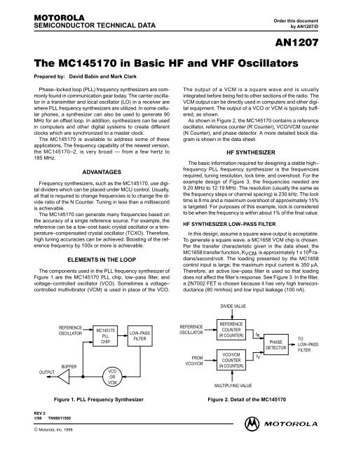
ELEMENTS IN THE LOOP<br />
<strong>The</strong> components used <strong>in</strong> the PLL frequency synthesizer of<br />
Figure 1 are the <strong>MC145170</strong> PLL chip, low–pass filter, <strong>and</strong><br />
voltage–controlled oscillator (VCO). Sometimes a voltage–<br />
controlled multivibrator (VCM) is used <strong>in</strong> place of the VCO.<br />
<strong>The</strong> output of a VCM is a square wave <strong>and</strong> is usually<br />
<strong>in</strong>tegrated before be<strong>in</strong>g fed to other sections of the radio. <strong>The</strong><br />
VCM output can be directly used <strong>in</strong> computers <strong>and</strong> other digital<br />
equipment. <strong>The</strong> output of a VCO or VCM is typically buffered,<br />
as shown.<br />
As shown <strong>in</strong> Figure 2, the <strong>MC145170</strong> conta<strong>in</strong>s a reference<br />
oscillator, reference counter (R Counter), VCO/VCM counter<br />
(N Counter), <strong>and</strong> phase detector. A more detailed block diagram<br />
is shown <strong>in</strong> the data sheet.<br />
<strong>HF</strong> SYNTHESIZER<br />
<strong>The</strong> basic <strong>in</strong>formation required for design<strong>in</strong>g a stable high–<br />
frequency PLL frequency synthesizer is the frequencies<br />
required, tun<strong>in</strong>g resolution, lock time, <strong>and</strong> overshoot. For the<br />
example design of Figure 3, the frequencies needed are<br />
9.20 MHz to 12.19 MHz. <strong>The</strong> resolution (usually the same as<br />
the frequency steps or channel spac<strong>in</strong>g) is 230 kHz. <strong>The</strong> lock<br />
time is 8 ms <strong>and</strong> a maximum overshoot of approximately 15%<br />
is targeted. For purposes of this example, lock is considered<br />
to be when the frequency is with<strong>in</strong> about 1% of the f<strong>in</strong>al value.<br />
<strong>HF</strong> SYNTHESIZER LOW–PASS FILTER<br />
In this design, assume a square wave output is acceptable.<br />
To generate a square wave, a MC1658 VCM chip is chosen.<br />
Per the transfer characteristic given <strong>in</strong> the data sheet, the<br />
MC1658 transfer function, KVCM, is approximately 1 x 10⁸ radians/second/volt.<br />
<strong>The</strong> load<strong>in</strong>g presented by the MC1658<br />
control <strong>in</strong>put is large; the maximum <strong>in</strong>put current is 350 µA.<br />
<strong>The</strong>refore, an active low–pass filter is used so that load<strong>in</strong>g<br />
does not affect the filter’s response. See Figure 3. In the filter,<br />
a 2N7002 FET is chosen because it has very high transconductance<br />
(80 mmhos) <strong>and</strong> low <strong>in</strong>put leakage (100 nA).<br />
DIVIDE VALUE<br />
OUTPUT<br />
REFERENCE<br />
OSCILLATOR<br />
BUFFER<br />
<strong>MC145170</strong><br />
PLL<br />
CHIP<br />
VCO<br />
OR<br />
VCM<br />
LOW–PASS<br />
FILTER<br />
REFERENCE<br />
OSCILLATOR<br />
FROM<br />
VCO/VCM<br />
REFERENCE<br />
COUNTER<br />
(R COUNTER)<br />
VCO/VCM<br />
COUNTER<br />
(N COUNTER)<br />
MULTIPLYING VALUE<br />
fR<br />
fV<br />
PHASE<br />
DETECTOR<br />
TO<br />
LOW–PASS<br />
FILTER<br />
Figure 1. PLL Frequency Synthesizer<br />
Figure 2. Detail of the <strong>MC145170</strong><br />
REV 2<br />
1/98 TN98011500<br />
© Motorola, Inc. 1998<br />
MOTOROLA<br />
AN1207<br />
1
+ 5 V + 5 V + 5 V<br />
4.6 MHz<br />
1 – 2 V p–p<br />
SOURCE<br />
MCU<br />
0.01 µF<br />
0.01 µF<br />
1 MΩ<br />
DATA IN<br />
ENABLE<br />
CLOCK<br />
1.5 kΩ<br />
PLL<br />
R2 BIAS<br />
FREQUENCY<br />
SYNTHESIZER<br />
LOW–PASS 2.4 kΩ<br />
FILTER<br />
1 16 1<br />
0.01 µF C 1 µF<br />
PDout R1<br />
2N7002<br />
<strong>MC145170</strong><br />
1.8 MΩ<br />
8 9<br />
0.01<br />
µF<br />
VCM<br />
MC1658<br />
16<br />
8 9<br />
47 pF<br />
0.01 µF<br />
0.01 µF<br />
1 MΩ<br />
1 MΩ<br />
MC74HCU04<br />
A<br />
LOW–PASS FILTER<br />
0.01 µF<br />
510 Ω<br />
0.01 µF<br />
PULLDOWN<br />
B<br />
BUFFER/FILTER<br />
MC74HCU04<br />
OUTPUT<br />
Figure 3. <strong>HF</strong> Synthesizer<br />
In order to calculate the average divide value for the N<br />
Counter, follow this procedure. First, determ<strong>in</strong>e the average<br />
frequency; this is (12.19 + 9.2)/2 = 10.695 MHz or approximately<br />
10.7 MHz. Next, divide this frequency by the resolution:<br />
10.7 MHz/230 kHz = about 47.<br />
Next, reference application note AN535 (see book<br />
DL136/D Rev 3 or 4). <strong>The</strong> active filter chosen takes the form<br />
shown <strong>in</strong> Figure 9 of the application note. This filter is used<br />
with the s<strong>in</strong>gle–ended phase detector output of the<br />
<strong>MC145170</strong>, PDout. <strong>The</strong> phase detector associated with PDout<br />
has a ga<strong>in</strong> Kφ = VDD/4π. For a supply of 5 V, this is 5/4π =<br />
0.398 V/rad. <strong>The</strong> system’s step response is shown <strong>in</strong> Figure<br />
4. To achieve about 15% overshoot, a damp<strong>in</strong>g factor of 0.8<br />
is used. This causes frequency to settle to with<strong>in</strong> 1% at ωnt<br />
= 5.5.<br />
<strong>The</strong> <strong>in</strong>formation up to this po<strong>in</strong>t is as follows.<br />
fref = 230 kHz<br />
fVCM = 9.2 to 12.19 MHz; the average is 10.7 MHz,<br />
average N = 47<br />
power supply = 5 V for the phase detector<br />
KVCM = 1 x 10⁸ rad/s/V<br />
overshoot = approximately 15%, yields a damp<strong>in</strong>g<br />
factor = 0.8<br />
lock time t = 8 ms settl<strong>in</strong>g to with<strong>in</strong> 1%, ωnt = 5.5<br />
Kφ or Kp = 0.398 V/rad.<br />
From the application note, equation 61, ωn = 5.5/t =<br />
5.5/0.008 = 687.5 rad/s.<br />
Equation 59 is R1C = (Kp Kv)/ωn 2 N<br />
= (0.398 x 1 x 108)/687.52 x 47<br />
= 1.79<br />
Equation 59 is used because of the high–ga<strong>in</strong> FET.<br />
Next, the capacitor C is picked to be 1 µF. <strong>The</strong>refore,<br />
R1 = 1.79/C which is 1.79 MΩ. <strong>The</strong> st<strong>and</strong>ard value of 1.8 MΩ<br />
is used for R1.<br />
Equation 63 is R2<br />
= (2ζ)/C ωn<br />
= (2 x 0.8)/(1 x 10–6 x 687.5)<br />
= 2.33 kΩ.<br />
A st<strong>and</strong>ard value for R2 of 2.4 kΩ is utilized.<br />
(t), NORMALIZED OUTPUT FREQUENCY<br />
θ o<br />
1.8<br />
1.7<br />
1.6<br />
1.5<br />
1.4<br />
1.3<br />
1.2<br />
1.1<br />
1.0<br />
0.9<br />
0.8<br />
0.7<br />
0.6<br />
0.5<br />
0.4<br />
0.3<br />
0.2<br />
0.1<br />
0<br />
ζ = 0.1<br />
0.2<br />
0.8<br />
1.0<br />
2.0<br />
0.3<br />
0.4<br />
0.5<br />
0.6<br />
0.7<br />
0 1.0 2.0 3.0 4.0 5.0 6.0 7.0 8.0 9.0 10 11 12 13 14<br />
ωnt<br />
Figure 4. Type 2 Second Order Step Response<br />
<strong>HF</strong> SYNTHESIZER PROGRAMMING<br />
Programm<strong>in</strong>g the <strong>MC145170</strong> is straightforward. <strong>The</strong> three<br />
registers may be programmed <strong>in</strong> a byte–oriented fashion.<br />
<strong>The</strong> registers reta<strong>in</strong> their values as long as power is applied.<br />
Thus, usually both the C <strong>and</strong> R Registers are programmed<br />
just once, right after power up.<br />
AN1207<br />
2<br />
MOTOROLA
<strong>The</strong> C Register, which configures the device, is programmed<br />
with $C0 (1 byte). This sets the phase detector to<br />
the proper polarity <strong>and</strong> activates PDout. This also turns off the<br />
unused outputs. <strong>The</strong> phase detector polarity is determ<strong>in</strong>ed by<br />
the filter <strong>and</strong> the VCM. For this example, the MC1658 data<br />
sheet shows that a higher voltage level is needed if speed is<br />
to be <strong>in</strong>creased. However, the low–pass filter <strong>in</strong>verts the signal<br />
from the phase detector (due to the active element configuration).<br />
<strong>The</strong>refore, the programm<strong>in</strong>g of the polarity for the<br />
phase detector means that the POL bit must be a “1.”<br />
<strong>The</strong> R Register is programmed for a divide value that<br />
results <strong>in</strong> the proper frequency at the phase detector reference<br />
<strong>in</strong>put. In this case, 230 kHz is needed. <strong>The</strong>refore, with<br />
the 4.6 MHz source shown <strong>in</strong> Figure 3, the R Register needs<br />
a value of $000014 (3 bytes, 20 <strong>in</strong> decimal).<br />
<strong>The</strong> N Register determ<strong>in</strong>es the frequency tuned. Tun<strong>in</strong>g<br />
9.2 MHz requires the proper value for N to multiply up the<br />
reference of 230 kHz to 9.2 MHz. This is 40 decimal. For<br />
12.19 MHz, the value is 53 decimal. To tune over the range,<br />
change the value <strong>in</strong> the N Register with<strong>in</strong> the range of 40 to 53<br />
with a 2–byte transfer. Table 1 shows the possible frequencies.<br />
MOTOROLA<br />
Table 1. <strong>The</strong> <strong>HF</strong> Oscillator Frequencies<br />
N Value<br />
Frequency, MHz<br />
40 9.20<br />
41 9.43<br />
42 9.66<br />
43 9.89<br />
44 10.12<br />
45 10.35<br />
46 10.58<br />
47 10.81<br />
48 11.04<br />
49 11.27<br />
50 11.50<br />
51 11.73<br />
52 11.96<br />
53 12.19<br />
EXTRA FILTERING FOR THE <strong>HF</strong> LOOP<br />
When the <strong>HF</strong> oscillator was built, the proper frequencies<br />
could not be tuned. <strong>The</strong> output of the MC1658 was exam<strong>in</strong>ed<br />
with an oscilloscope <strong>and</strong> the switch<strong>in</strong>g edges were discovered<br />
to be “ragged.” That is, the output did not appear to be a<br />
square wave with clean transitions.<br />
<strong>The</strong> f<strong>in</strong> <strong>in</strong>put of the <strong>MC145170</strong> is sensitive to 500 mV p–p<br />
signals, <strong>and</strong> the ragged edges were be<strong>in</strong>g amplified <strong>and</strong><br />
counted down by the N Counter. <strong>The</strong>refore, the edges needed<br />
clean<strong>in</strong>g up. One method would have been to add a low–<br />
pass filter between the MC1658 <strong>and</strong> <strong>MC145170</strong>. However,<br />
because an additional buffer was needed elsewhere <strong>in</strong> the<br />
circuit, an MC74HCU04 <strong>in</strong>verter was used <strong>in</strong> place of the filter.<br />
This <strong>in</strong>verter’s frequency response is low enough to clean<br />
up the ragged edges. That is, filter<strong>in</strong>g of the ragged edges<br />
occurred, <strong>and</strong> the output had smoother transitions. As mentioned<br />
previously, one of the elements <strong>in</strong> the <strong>in</strong>verter package<br />
was used to buffer the output of the VCM before feed<strong>in</strong>g it to<br />
the outside world. See Figure 3.<br />
V<strong>HF</strong> SYNTHESIZER<br />
<strong>The</strong> <strong>MC145170</strong> may be used <strong>in</strong> V<strong>HF</strong> designs, also. <strong>The</strong><br />
range for this next example is 140 to 160 MHz <strong>in</strong> 100 kHz<br />
<strong>in</strong>crements.<br />
V<strong>HF</strong> SYNTHESIZER LOW–PASS FILTER<br />
To illustrate design with the doubled–ended phase detector,<br />
the φR <strong>and</strong> φV outputs are used. This requires an operational<br />
amplifier, as shown <strong>in</strong> Figure 5. From the design<br />
guidel<strong>in</strong>es shown <strong>in</strong> the <strong>MC145170</strong> data sheet, the follow<strong>in</strong>g<br />
equations are used:<br />
ωn =<br />
KφKVCO<br />
N C R1<br />
ζ = ω n R2C<br />
damp<strong>in</strong>g factor<br />
(2)<br />
2<br />
where, from the data sheet, the equation for the φR <strong>and</strong> φV<br />
phase detector,<br />
Kφ = V DD 5<br />
= = 0.796 V/rad<br />
(3)<br />
2π 2π<br />
ζ = 0.707,<br />
<strong>and</strong><br />
ωn = 2πf R<br />
50<br />
KVCO = 2π ∆ f VCO<br />
∆ VVCO<br />
2π x 100 kHz<br />
= = 12,566 rad/s<br />
50<br />
=<br />
2π x (160 – 140 MHz)<br />
10 – 2<br />
= 1.57 x 10⁷ rad/s/V (5)<br />
<strong>The</strong> control voltage range on the <strong>in</strong>put to the VCO is picked<br />
to be 2 to 10 V.<br />
<strong>The</strong> average frequency = (140 + 160)/2 = 150 MHz. <strong>The</strong>refore,<br />
the average N = 1500.<br />
<strong>The</strong> above choices for ζ <strong>and</strong> ωn are rules of thumb that are<br />
a good design start<strong>in</strong>g po<strong>in</strong>t. A larger ωn value results <strong>in</strong> faster<br />
loop lock times <strong>and</strong> higher reference frequency VCO<br />
sideb<strong>and</strong>s for similar sideb<strong>and</strong> filter<strong>in</strong>g. (See Advanced<br />
Considerations.)<br />
Choos<strong>in</strong>g C1 to be 4700 pF, R1 is calculated from the<br />
rearranged expression for ωn as:<br />
R1= K φKVCO (0.796 V/rad)(1.57 x 107 rad/s/V)<br />
=<br />
C1ωnN<br />
2<br />
(4700 pF)(12,566 rad/s)2 (1500)<br />
= 11.23 kΩ<br />
(6)<br />
<strong>The</strong>refore, chose an 11 kΩ st<strong>and</strong>ard value resistor.<br />
R2 is determ<strong>in</strong>ed from:<br />
2ζ<br />
R2 = =<br />
ωnC1<br />
(2)(0.707)<br />
(12,566)(4700 pF)<br />
= 23.94 kΩ or<br />
24 kΩ (st<strong>and</strong>ard value)<br />
V<strong>HF</strong> SYNTHESIZER EXTRA FILTERING<br />
For more dem<strong>and</strong><strong>in</strong>g applications, extra filter<strong>in</strong>g is sometimes<br />
added. This reduces the VCO sideb<strong>and</strong>s caused by a<br />
small amount of the reference frequency feed<strong>in</strong>g through the<br />
filter. One form of this filter<strong>in</strong>g consists of spitt<strong>in</strong>g R1 <strong>in</strong>to two<br />
resistors; each resistor is one–half the value of R1, as <strong>in</strong>dicated<br />
by R1/2 <strong>in</strong> Figure 5. Capacitors CC are added from the<br />
(1)<br />
(4)<br />
(7)<br />
AN1207<br />
3
20 pF<br />
1 MHz<br />
Y1<br />
1 MΩ<br />
1 16<br />
<strong>MC145170</strong><br />
+ 5 V<br />
4 x 5.6 kΩ<br />
2 x 1500 pF<br />
R1/2<br />
R1/2<br />
CC<br />
R1/2 R1/2<br />
CC<br />
24 kΩ 4700 pF<br />
+ 12 V<br />
–<br />
LF351<br />
+<br />
24 kΩ<br />
20 pF 100 pF<br />
8 9<br />
1 kΩ<br />
4700 pF<br />
OUTPUT<br />
DATA OUT<br />
CLK<br />
EN<br />
DATA IN<br />
TEST POINT<br />
(LOCK DETECT)<br />
+ 5 V<br />
+ 5 V<br />
1<br />
14<br />
20 nH<br />
2 x MV2115<br />
R14<br />
10 kΩ<br />
MC1648<br />
1000 pF<br />
7 8<br />
0.1 µF 390 pF<br />
C5<br />
Figure 5. V<strong>HF</strong> Synthesizer<br />
midpo<strong>in</strong>ts to ground to further filter the reference sideb<strong>and</strong>s.<br />
<strong>The</strong> value of CC is chosen so that the corner frequency of this<br />
added network does not significantly affect the orig<strong>in</strong>al loop<br />
b<strong>and</strong>width ωB.<br />
<strong>The</strong> rule of thumb for an <strong>in</strong>itial value is CC = 4 / ( R1 ωRC),<br />
where ωRC is the filter cutoff frequency. A good value is to<br />
choose ωRC to be 10 x ωB, so as to not significantly impact the<br />
orig<strong>in</strong>al filter.<br />
ωB = ωn 1 + 2ζ2 + 2 + 4ζ2 + 4ζ4 (8)<br />
= 12,566 1+(2)(0.707)2+ 2+(4)(0.707)2+ (4)(0.707)4<br />
= 25,860 rad/s<br />
ωRC = 10 ωB = (10)(25,860) = 258,600 rad/s<br />
4<br />
4<br />
CC = =<br />
R1ωRC (11.23 kΩ)(258,600 rad/s)<br />
= 1377 pF ≈ 1500 pF<br />
(9)<br />
(10)<br />
<strong>The</strong>re is also a filter formed at the <strong>in</strong>put to the VCO. Aga<strong>in</strong>,<br />
this should be selected to ensure that it does not significantly<br />
affect the loop b<strong>and</strong>width. For this example, the filter is dom<strong>in</strong>ated<br />
by R14 with C5. <strong>The</strong> capacitance of the varactors (<strong>in</strong><br />
series with the rest of the circuit) is much smaller than C5 <strong>and</strong><br />
can therefore be neglected for this calculation.<br />
As above, let ωRC = 258,600 rad/s be the cutoff of this filter.<br />
R14 is chosen to be 10 kΩ. <strong>The</strong>refore,<br />
1<br />
1<br />
C5 = =<br />
ωRCR14 (258,600)(10 kΩ)<br />
= 387 pF ≈ 390 pF<br />
THE VARACTOR<br />
(11)<br />
<strong>The</strong> MV2115 was selected for its tun<strong>in</strong>g ratio of 2.6 to 1.<br />
<strong>The</strong> capacitance can be changed from 49.1 pF to 127.7 pF<br />
over a reverse bias sw<strong>in</strong>g of 2 to 30 volts. Contact your Motorola<br />
representative for <strong>in</strong>formation regard<strong>in</strong>g the MV2115 varactor<br />
diode.<br />
For example, three parameters are considered.<br />
CT = Nom<strong>in</strong>al capacitance<br />
CR = Capacitance ratio<br />
fR = Frequency ratio<br />
CR= C vm<strong>in</strong><br />
=<br />
Cvmax<br />
where ρ = the capacitance exponent<br />
Vmax<br />
Vm<strong>in</strong><br />
ρ<br />
(12)<br />
AN1207<br />
4<br />
MOTOROLA
<strong>The</strong>refore,<br />
MOTOROLA<br />
30 ρ<br />
CR = 2.6 = (13)<br />
2<br />
log(2.6) = ρlog(15)<br />
ρ = log(2.6)/log(15) = 0.3528<br />
Us<strong>in</strong>g the nom<strong>in</strong>al capacitance of 100 pF at 4 volts:<br />
Solv<strong>in</strong>g for Cvmax:<br />
Solv<strong>in</strong>g for Cvm<strong>in</strong>:<br />
THE VCO<br />
100 pF =<br />
Cvmax<br />
100 pF<br />
= 1.382<br />
Cvmax<br />
10 0.3528<br />
4 V<br />
100 pF<br />
= 72.4 pF<br />
1.382<br />
2.6 = C vm<strong>in</strong><br />
49.1 pF<br />
Cvm<strong>in</strong> = (2.6)(49.1 pF)<br />
Cvm<strong>in</strong> = 127.7 pF<br />
(14)<br />
(15)<br />
(16)<br />
(17)<br />
For convenience, the MC1648 VCO is selected. <strong>The</strong> tun<strong>in</strong>g<br />
range of the VCO may be calculated as<br />
fmax (Cdmax + Cs)0.5<br />
=<br />
(18)<br />
fm<strong>in</strong> (Cdm<strong>in</strong> + Cs)0.5<br />
where<br />
1<br />
fm<strong>in</strong> =<br />
(19)<br />
2π[L(Cdmax + Cs)]0.5<br />
As shown <strong>in</strong> Figure 8 of the data sheet, the VCO tank circuit<br />
is comprised of two varactors <strong>and</strong> an <strong>in</strong>ductor. Typically, a<br />
s<strong>in</strong>gle varactor might be used <strong>in</strong> either a series or parallel<br />
configuration. However, the second varactor has a two–fold<br />
purpose. First, if the 10 kΩ isolat<strong>in</strong>g impedance is left <strong>in</strong> place,<br />
the varactors add <strong>in</strong> series for a smaller capacitance. Second,<br />
the added varactor acts to elim<strong>in</strong>ate distortion due to<br />
the tank voltage chang<strong>in</strong>g.<br />
<strong>The</strong>refore, with the two varactors <strong>in</strong> series, Cdmax′ =<br />
Cdmax/2. <strong>The</strong> shunt capacitance (<strong>in</strong>put plus external capacitance)<br />
is symbolized by Cs.<br />
<strong>The</strong>refore, solv<strong>in</strong>g for the <strong>in</strong>ductance:<br />
1<br />
L =<br />
= 19.9 nH ≈ 20 nH (20)<br />
(2πfm<strong>in</strong>)2(Cdmax′ + Cs)<br />
<strong>The</strong> Q of the <strong>in</strong>ductor should be more than 100 for best performance.<br />
1<br />
fm<strong>in</strong> =<br />
= 135 MHz (21)<br />
2π[(19.9 nH)(69.85 pF)]0.5<br />
1<br />
fmax =<br />
= 173 MHz (22)<br />
2π[(19.9 nH)(42.2 pF)]0.5<br />
<strong>The</strong> frequency ratio is 1.5 to 1 <strong>and</strong> is impacted by the tun<strong>in</strong>g<br />
range of the MV2115 varactor diode used <strong>in</strong> the tank circuit.<br />
<strong>The</strong>refore, the required range of 140 to 160 MHz is not limited<br />
by this VCO design.<br />
A pc board should be used to obta<strong>in</strong> favorable results with<br />
this V<strong>HF</strong> circuit. <strong>The</strong> lead lengths <strong>in</strong> the tank circuit should be<br />
kept short to m<strong>in</strong>imize parasitic <strong>in</strong>ductance. <strong>The</strong> length of the<br />
trace from the VCO output to the PLL <strong>in</strong>put should be kept as<br />
short as possible. In addition, use of surface–mount components<br />
is recommended to help m<strong>in</strong>imize strays.<br />
V<strong>HF</strong> SYNTHESIZER PROGRAMMING<br />
Aga<strong>in</strong>, programm<strong>in</strong>g the three registers of the <strong>MC145170</strong><br />
is straightforward. Also, usually both the C <strong>and</strong> the R Registers<br />
are programmed only once, after power up.<br />
<strong>The</strong> C Register configures the device <strong>and</strong> is programmed<br />
with $80 (1 byte). This sets the phase detector to the correct<br />
polarity <strong>and</strong> activates the φR <strong>and</strong> φV outputs while turn<strong>in</strong>g off<br />
the other outputs. Like the <strong>HF</strong> oscillator, the phase detector<br />
polarity is determ<strong>in</strong>ed by how the filter is hooked up <strong>and</strong> the<br />
VCO.<br />
<strong>The</strong> R Register is programmed for a divide value that<br />
delivers the proper frequency at the phase detector reference<br />
<strong>in</strong>put. In this case, 100 kHz is needed. <strong>The</strong>refore, with the<br />
1 MHz crystal shown, the R Register needs a value of<br />
$00000A (3 bytes, 10 <strong>in</strong> decimal).<br />
<strong>The</strong> N Register determ<strong>in</strong>es the frequency tuned. To tune<br />
140 MHz, the value required for N to multiply up the reference<br />
of 100 kHz to 140 MHz is 1400 decimal. For 160 MHz, the<br />
value is 1600 decimal. To tune over the range, simply change<br />
the value <strong>in</strong> the N Register with a 2–byte transfer.<br />
ADVANCED CONSIDERATIONS<br />
<strong>The</strong> circuit of Figure 5 may not function at very–high temperature.<br />
<strong>The</strong> reason is that the <strong>MC145170</strong> is guaranteed to<br />
a maximum frequency of 160 MHz at 85°C. <strong>The</strong>refore, there<br />
is no marg<strong>in</strong> for overshoot (reference Figure 4) at high temperature.<br />
<strong>The</strong>re are two possible solutions: (1) use the<br />
<strong>MC145170</strong>–1 or <strong>MC145170</strong>–2 which are rated to 185 MHz,<br />
or (2) limit the tun<strong>in</strong>g to less than 160 MHz.<br />
Operational amplifiers are usually too noisy for critical applications.<br />
<strong>The</strong>refore, if an active element is required <strong>in</strong> the <strong>in</strong>tegrator,<br />
one or more discrete transistors are utilized. <strong>The</strong>se<br />
may be FETs or bipolar devices. However, active filter elements<br />
are not needed if the VCO load<strong>in</strong>g is not severe, such<br />
as is encountered with most discrete VCO designs. Because<br />
active elements add noise, some performance parameters<br />
are improved if they are not used. On the other h<strong>and</strong>, an active<br />
filter can be used to scale up the VCO control voltage. For<br />
example, to tune a wide range, the control voltage may have<br />
to range up to 10 V. For a 5 V PLL output, this would be scaled<br />
by 2x via use of active elements.<br />
Some applications have requirements that must be met <strong>in</strong><br />
the areas of phase noise <strong>and</strong> reference suppression. <strong>The</strong>se<br />
parameters are <strong>in</strong> conflict with fast lock times. That is, as lock<br />
times are reduced, reference suppression becomes more difficult.<br />
Both reference suppression <strong>and</strong> phase noise are advanced<br />
areas that are covered <strong>in</strong> several publications. As an<br />
example, consider that the VCO <strong>in</strong>put voltage range for<br />
the above V<strong>HF</strong> loop was merely picked to be 8 V. Advanced<br />
AN1207<br />
5
techniques dem<strong>and</strong> a trade off between this voltage range<br />
<strong>and</strong> the spectral purity of the VCO output. This is because the<br />
lower the control voltage range, the more sensitive the VCO<br />
is to noise com<strong>in</strong>g <strong>in</strong>to its control <strong>in</strong>put.<br />
A VCO IC may not offer enough performance for some<br />
applications. <strong>The</strong>refore, the VCO may have to be designed<br />
from discrete components.<br />
Figure 6 shows the performance of the V<strong>HF</strong> Oscillator<br />
prototype on a spectrum analyzer. Note that the reference<br />
sideb<strong>and</strong>s appear at 100 kHz as expected, <strong>and</strong> are 50 dB<br />
down.<br />
REFERENCES<br />
Motorola data sheet <strong>MC145170</strong>/D<br />
Motorola data sheet <strong>MC145170</strong>–1/D<br />
Motorola data sheet <strong>MC145170</strong>–2/D<br />
Motorola application note AN535/D<br />
10 dB PER DIVISION<br />
100 kHz<br />
CENTER = 150 MHz, SPAN = 250 kHz<br />
100 kHz<br />
Figure 6. V<strong>HF</strong> Oscillator Performance<br />
Motorola reserves the right to make changes without further notice to any products here<strong>in</strong>. Motorola makes no warranty, representation or guarantee regard<strong>in</strong>g<br />
the suitability of its products for any particular purpose, nor does Motorola assume any liability aris<strong>in</strong>g out of the application or use of any product or circuit, <strong>and</strong><br />
specifically disclaims any <strong>and</strong> all liability, <strong>in</strong>clud<strong>in</strong>g without limitation consequential or <strong>in</strong>cidental damages. “Typical” parameters which may be provided <strong>in</strong> Motorola<br />
data sheets <strong>and</strong>/or specifications can <strong>and</strong> do vary <strong>in</strong> different applications <strong>and</strong> actual performance may vary over time. All operat<strong>in</strong>g parameters, <strong>in</strong>clud<strong>in</strong>g “Typicals”<br />
must be validated for each customer application by customer’s technical experts. Motorola does not convey any license under its patent rights nor the rights of<br />
others. Motorola products are not designed, <strong>in</strong>tended, or authorized for use as components <strong>in</strong> systems <strong>in</strong>tended for surgical implant <strong>in</strong>to the body, or other<br />
applications <strong>in</strong>tended to support or susta<strong>in</strong> life, or for any other application <strong>in</strong> which the failure of the Motorola product could create a situation where personal <strong>in</strong>jury<br />
or death may occur. Should Buyer purchase or use Motorola products for any such un<strong>in</strong>tended or unauthorized application, Buyer shall <strong>in</strong>demnify <strong>and</strong> hold Motorola<br />
<strong>and</strong> its officers, employees, subsidiaries, affiliates, <strong>and</strong> distributors harmless aga<strong>in</strong>st all claims, costs, damages, <strong>and</strong> expenses, <strong>and</strong> reasonable attorney fees<br />
aris<strong>in</strong>g out of, directly or <strong>in</strong>directly, any claim of personal <strong>in</strong>jury or death associated with such un<strong>in</strong>tended or unauthorized use, even if such claim alleges that<br />
Motorola was negligent regard<strong>in</strong>g the design or manufacture of the part. Motorola <strong>and</strong> are registered trademarks of Motorola, Inc. Motorola, Inc. is an Equal<br />
Opportunity/Affirmative Action Employer.<br />
Mfax is a trademark of Motorola, Inc.<br />
How to reach us:<br />
USA / EUROPE / Locations Not Listed: Motorola Literature Distribution; JAPAN: Nippon Motorola Ltd.; SPD, Strategic Plann<strong>in</strong>g Office; 4-32-1,<br />
P.O. Box 5405, Denver, Colorado, 80217. 1-303-675-2140 or 1-800-441-2447 Nishi-Got<strong>and</strong>a; Sh<strong>in</strong>agawa-ku, Tokyo 141, Japan. 81-3-5487-8488<br />
Mfax : RMFAX0@email.sps.mot.com – TOUCHTONE 1-602-244-6609 ASIA/PACIFIC: Motorola Semiconductors H.K. Ltd.; 8B Tai P<strong>in</strong>g Industrial Park,<br />
Motorola Fax Back System – US & Canada ONLY 1-800-774-1848 51 T<strong>in</strong>g Kok Road, Tai Po, N.T., Hong Kong. 852-26629298<br />
– http://sps.motorola.com /mfax /<br />
HOME PAGE : http://motorola.com/sps / CUSTOMER FOCUS CENTER: 1-800-521-6274<br />
AN1207<br />
6<br />
◊<br />
AN1207/D<br />
MOTOROLA