NEW DISCRETE DYNODE TOF DETECTOR
NEW DISCRETE DYNODE TOF DETECTOR
NEW DISCRETE DYNODE TOF DETECTOR

Create successful ePaper yourself
Turn your PDF publications into a flip-book with our unique Google optimized e-Paper software.
www.sge.com<br />
DETAILED PERFORMANCE CHARACTERISTICS OF A<br />
<strong>NEW</strong> <strong>DISCRETE</strong> <strong>DYNODE</strong><br />
<strong>TOF</strong> <strong>DETECTOR</strong><br />
Dick Stresau and Kevin L. Hunter<br />
ETP Electron Multipliers Pty. Ltd. Ermington, Australia<br />
Presented at The 47th ASMS Conference on Mass Spectroscopy and Allied Topics<br />
June 13-17, 1999, Dallas, Texas<br />
Electron<br />
Multipliers<br />
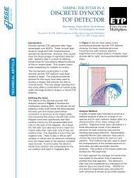
Why use a discrete dynode detector for<br />
<strong>TOF</strong>?<br />
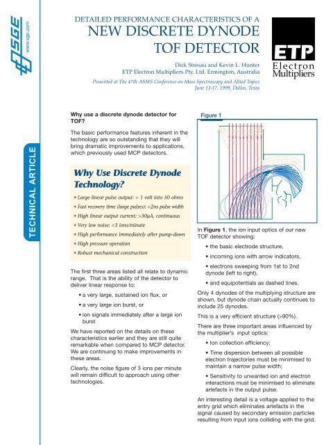
Figure 1<br />
TECHNICAL ARTICLE<br />
The basic performance features inherent in the<br />
technology are so outstanding that they will<br />
bring dramatic improvements to applications,<br />
which previously used MCP detectors.<br />
Why Use Discrete Dynode<br />
Technology?<br />
• Large linear pulse output: > 1 volt into 50 ohms<br />
• Fast recovery time (large pulses): 30µA, continuous<br />
• Very low noise: 90%).<br />
There are three important areas influenced by<br />
the multiplier’s input optics:<br />
• Ion collection efficiency;<br />
• Time dispersion between all possible<br />
electron trajectories must be minimised to<br />
maintain a narrow pulse width;<br />
• Sensitivity to unwanted ion and electron<br />
interactions must be minimised to eliminate<br />
artefacts in the output pulse.<br />
An interesting detail is a voltage applied to the<br />
entry grid which eliminates artefacts in the<br />
signal caused by secondary emission particles<br />
resulting from input ions colliding with the grid.
In Figure 2, Gain curve of DM152 demonstrating another<br />
of the new concepts we are incorporating in our new <strong>TOF</strong><br />
detectors. We have designed this detector to initially<br />
operate with an applied voltage of ~3kV, and with an<br />
upper limit, reached as the multiplier ages, of ~4.5kV.<br />
This increased voltage range enables significant<br />
improvements in both pulse width and multiplier aging<br />
characteristics. The choice of the upper limit was based<br />
on the voltage ratings of conventional vacuum<br />
feedthroughs.<br />
Figure 2<br />
1.E+08<br />
1.E+07<br />
Gain<br />
1.E+06<br />
1.E+05<br />
1.E+04<br />
2500 3000 3500 4000<br />
Applied Voltage (V)<br />
We have achieved the optimal initial operating voltage by<br />
selecting different active dynode materials for different<br />
parts of the multiplier dynode chain. The DM152 was<br />
designed to operate at a gain between 10 5 and 10 6 .<br />
A design optimized for 10 7 operation would require a<br />
simple change in dynode materials. By changing the<br />
combination of materials we can design a multiplier to<br />
operate at any required gain and still maintain optimal<br />
initial voltage<br />
Figure 3<br />
Figure 3 shows the influence of dynode size on the<br />
detector’s output pulse width including both calculated<br />
figures and data taken with 3 different multipliers. The<br />
pulse width at half maximum is plotted against dynode size.<br />
We have chosen the dynode size from one of our ’standard’<br />
<strong>TOF</strong> detectors, AF824, as the measurement unit for this<br />
data. The upper blue circle indicates the AF824 data.
The data all indicates that to achieve a narrow pulse<br />
width the multiplier’s dynode size should be as small as<br />
possible. We have chosen 40% of "the standard size" as<br />
a practical compromise between pulse width and<br />
manufacturing ease.<br />
This ‘40% size’ is not a fundamental size barrier. We<br />
expect to continue this shrinking process and further<br />
improve detector speed.<br />
In Figure 4, typical pulse from the DM152. These pulse<br />
measurements have been made by averaging a large<br />
number of single ion events.<br />
Figure 4<br />
7:58:44<br />
A: Average (1)<br />
1ns<br />
1.8mV<br />
As is well known, when the frequency components in a<br />
detector’s output signal exceed 100 Mhz, impedance<br />
matching and ringing become a major issue. We found it<br />
is important to mount the compensation circuit and an<br />
impedance matched connector directly on the multiplier.<br />
It is also important to insure that all cables and<br />
connectors between the detector and detection<br />
electronics have appropriately matched impedance.<br />
Any break in the chain of matched components can<br />
cause a signal reflection and lead to ringing.<br />
Figure 5 shows output circuit to minimise ringing. After<br />
trying a variety of ‘text book solutions’ we selected this<br />
circuit as the most effective in minimizing ringing.<br />
Essentially, capacitors are connected between each of<br />
the last several dynodes and the signal line’s shield. For<br />
this to be effective a matched impedance signal line must<br />
extend up to the detector.<br />
Figure 5<br />
1000 swps<br />
D17<br />
D18<br />
1.4 Megohm, typical<br />
D19<br />
D20<br />
D21<br />
D22<br />
2ns<br />
1250 sweeps: average low high signs<br />
ampl(1) 89.8mV 79.5 120.1 6.5<br />
width(1) 1.54ns 1.18 2.33 0.16<br />
rise(1) 1.51ns 0.84 3.19 8.16<br />
fall(1) 1.22ns 0.88 2.90 0.15<br />
area(1) -464.154 pVs -589.813 -413.500 19.765<br />
D23<br />
D24<br />
D25<br />
Collector<br />
10nf, 1kV<br />
3 places<br />
3.3nf, 2kV<br />
4 places<br />
Connector shield<br />
50 ohm impedance<br />
SMA connector<br />
Reducing the dynode size not only increases detector<br />
speed, it also enables designs with a small physical size.<br />
For the DM152 we have kept the ‘footprint’ small,<br />
33 x 33mm, and the active area large, 10 x 25mm.<br />
I should point out that within this active area the ion<br />
collection efficiency is ~90% verses the 50% or 60% of<br />
an MCP.<br />
Electronics are mounted directly on the multiplier section<br />
and serve a couple of different functions:<br />
• 1 - They support a zener diode chain along with<br />
associated capacitors which are part of the voltage<br />
distribution network for the dynodes.<br />
• 2 - They also include a compensation network that<br />
helps to couple the signal to the output cable and<br />
minimize ringing.<br />
In Figure 6, output circuit to control two processes that<br />
can limit the level of the multiplier’s output pulse:<br />
• voltage droop during a large pulse and<br />
• excessive space charge in the dynode area.<br />
Figure 6<br />
D17<br />
D18<br />
D19<br />
D20<br />
D21<br />
D22<br />
D23<br />
D24<br />
D25<br />
1.4 Megohm, typical<br />
130 volt zener<br />
180 volt zener<br />
270 v. zener<br />
3.3nf, 2kV<br />
4 places<br />
Collector<br />
10nf, 1kV<br />
3 places
Figure 7<br />
D17<br />
D18<br />
1.4 Megohm, typical<br />
D19<br />
D20<br />
D21<br />
D22<br />
D23<br />
D24<br />
D25<br />
Collector<br />
130 volt zener<br />
180 volt zener<br />
270 v. zener<br />
10nf, 1kV<br />
3 places<br />
47 ohms<br />
3.3nf, 2kV<br />
4 places<br />
Connector shield<br />
50 ohm impedance<br />
SMA connector<br />
Above diagram shows the output circuit used on the<br />
DM152 <strong>TOF</strong> detector. It combines the concepts shown in<br />
Figures 5 & 6 and is very effective in both controlling<br />
ringing and providing large linear pulses.<br />
The capacitors, in this case, are used to supply the<br />
dynodes with the extra charge that is extracted from the<br />
multiplier during a large pulse, since the resistor chain is<br />
too slow to for this purpose. This ensures that the<br />
dynode’s voltage level, and therefore its efficiency, is<br />
maintained during the pulse.<br />
Excessive space charge will both limit the size of a pulse<br />
and increase its width. It is strongly dependant on the<br />
inter-dynode field strength, and therefore, controlling<br />
dynode voltages will also minimise space charge effects.<br />
The voltage on the last 3 dynodes is fixed to<br />
progressively increased voltages with zener diodes to<br />
further minimises effects from space charge.<br />
Figure 8<br />
1<br />
16:33:42<br />
10ns<br />
5.0mV<br />
A: Hminimum (1)<br />
2mV<br />
10.0 #<br />
-0%/+0%<br />
inside 1000<br />
Figure 8 shows the pulse from a multiplier with no output<br />
circuit, showing near 100% ringing level.
In Figure 9, the pulse shape from the DM152 <strong>TOF</strong> detector which includes the output<br />
circuit. The top trace is a single pulse. The middle trace is the average of 1000 pulses,<br />
and the bottom curve has been expanded by 10X in the x scale so that we can see the<br />
residual ringing more clearly.<br />
Figure 9<br />
7:29:49<br />
1<br />
5ns<br />
5.0mV<br />
1000 swps<br />
A: Average (1)<br />
5ns<br />
5.0mV<br />
1000 swps<br />
B?A<br />
5ns<br />
0.50mV<br />
1000 swps<br />
We very consistently measure ringing levels of ~2% of the signal peak with 1.5 Ghz<br />
bandwidth electronics as shown here. This wide bandwidth system provides a very<br />
severe test for this measurement. Another way of significantly minimising ringing is to<br />
reduce the bandwidth of the detection electronics. To achieve the optimal performance<br />
in a <strong>TOF</strong> system the instrument’s bandwidth should be just wide enough to achieve the<br />
required time resolution.<br />
We have looked at the details of several different areas in the design of the DM152 <strong>TOF</strong><br />
Detector. We have achieved superior performance by focussing design and<br />
development effort into several distinct areas. The methods reviewed have contributed<br />
to the DM152’s outstanding performance in the areas of:<br />
• Operational life<br />
• Pulse width<br />
• Ringing<br />
• Linearity<br />
The unusual combination of superior performance characteristics for the DM152 will<br />
lead to its use in a wide variety of applications.<br />
A DIVISION OF SGE GROUP OF COMPANIES<br />
Electron<br />
Multipliers<br />
www.etpsci.com<br />
SGE International Pty. Ltd.<br />
Tel: +61 (0) 3 9837 4200<br />
Fax: +61 (0) 3 9874 5672<br />
Email: techsupport@etpsci.com<br />
SGE, Incorporated (USA)<br />
Toll Free: (800) 945 6154<br />
Fax: (512) 836 9159<br />
Email: usa@sge.com<br />
© Copyright 2001 SGE International Pty. Ltd. All rights reserved. TA-0096-A<br />
SGE Europe Ltd<br />
Tel: +44 (0) 1908 568844<br />
Fax: +44 (0) 1908 566790<br />
Email: uk@sge.com<br />
www.sge.com