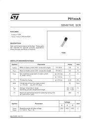
POSITIVE VOLTAGE REGULATORS - Pira.cz
POSITIVE VOLTAGE REGULATORS - Pira.cz
POSITIVE VOLTAGE REGULATORS - Pira.cz

You also want an ePaper? Increase the reach of your titles
YUMPU automatically turns print PDFs into web optimized ePapers that Google loves.
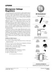
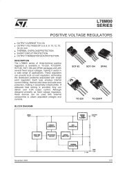
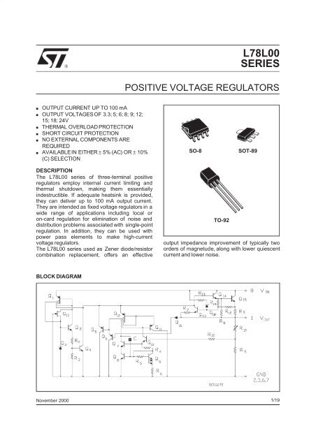
®L78L00SERIES<strong>POSITIVE</strong> <strong>VOLTAGE</strong> <strong>REGULATORS</strong>■ OUTPUT CURRENT UP TO 100 mA■ OUTPUT <strong>VOLTAGE</strong>SOF 3.3; 5; 6; 8; 9; 12;15; 18; 24V■ THERMAL OVERLOAD PROTECTION■ SHORT CIRCUIT PROTECTION■ NO EXTERNAL COMPONENTS AREREQUIRED■ AVAILABLEIN EITHER ± 5% (AC) OR ± 10%(C) SELECTIONSO-8SOT-89DESCRIPTIONThe L78L00 series of three-terminal positiveregulators employ internal current limiting andthermal shutdown, making them essentiallyindestructible. If adequate heatsink is provided,they can deliver up to 100 mA output current.They are intended as fixed voltage regulators in awide range of applications including local oron-card regulation for elimination of noise anddistribution problems associated with single-pointregulation. In addition, they can be used withpower pass elements to make high-currentvoltage regulators.The L78L00 series used as Zener diode/resistorcombination replacement, offers an effectiveTO-92output impedance improvement of typically twoorders of magnetude, along with lower quiescentcurrent and lower noise.BLOCK DIAGRAMNovember 20001/19
L78L00ABSOLUTE MAXIMUM RATINGSymbol Parameter Value UnitV i DC Input Voltage V o = 3.3 V to 9 V 30 VV o = 12 V to 15 V 35 VVo = 18 V to 24 V 40 VI o Output Current 100 mAP tot Power Dissipation Internally limited (*)T stg Storage Temperature Range - 40 to 150o CT opOperating Junction Temperature RangeFor L78L00C, L78L00ACFor L78L00AB0to125-40to125(*) Our SO-8 package used for Voltage Regulators is modified internally to have pins 2, 3, 6 and 7 electrically commoned to the die attachflag. This particular frame decreases the total thermal resistance of the package and increases its ability to dissipate power when anappropriate area of copper on the printed circuit board is available for heatsinking. The external dimensions are the same as for the standardSO-8o Co CTHERMAL DATASymbol Parameter SO-8 TO-92 SOT-89 UnitR thj-caseJunction-case 2015o C/WR thj-ambThermal ResistanceThermal Resistance Junction-ambientMaxMax 55 (*) 200o C/W(*) Considering 6cm 2 of copper Board heat-sinkTEST CIRCUITS2/19
L78L00ELECTRICAL CHARACTERISTICS FOR L78L05 (refer to the test circuits, Tj = 0 to 125 o C,Vi = 10V, Io = 40 mA, Ci = 0.33 µF, Co = 0.1 µF unless otherwise specified)Symbol Parameter Test Conditions Min. Typ. Max. UnitV o Output Voltage T j =25 o C 4.6 5 5.4 VVo Output Voltage Io = 1 to 40 mA Vi = 7 to 20 VI o = 1 to 70 mA V i =10V∆V o Line Regulation V i = 7 to 20 V T j =25 o CV i = 8 to 20 V T j =25 o C∆Vo Load Regulation I o = 1 to 100 mA T j =25 o CI o = 1 to 40 mA T j =25 o CI d Quiescent Current T j =25 o CT j = 125 o C∆I d Quiescent Current Change I o = 1 to 40 mA 0.2 mA∆I d Quiescent Current Change V i = 8 to 20 V 1.5 mAeN Output Noise Voltage B = 10Hz to 100KHz T j =25 o C 40 µVSVR Supply Voltage Rejection I o = 40 mA f = 120 Hz T j =25 o C 40 49 dBV i = 8 to 18 VV d Dropout Voltage 1.7 V4.54.55.55.5200150603065.5VVmVmVmVmVmAmAELECTRICAL CHARACTERISTICS FOR L78L06 (refer to the test circuits, Tj = 0 to 125 o C,Vi = 12V, Io = 40 mA, Ci = 0.33 µF, Co = 0.1 µF unless otherwise specified)Symbol Parameter Test Conditions Min. Typ. Max. UnitV o Output Voltage T j =25 o C 5.52 6 6.48 VV o Output Voltage I o = 1 to 40 mA V i = 8.5 to 20 VI o = 1 to 70 mA V i =12V∆V o Line Regulation V i = 8.5 to 20 V T j =25 o CV i = 9 to 20 V T j =25 o C∆V o Load Regulation I o = 1 to 100 mA T j =25 o CI o = 1 to 40 mA T j =25 o CI d Quiescent Current T j =25 o CT j = 125 o C∆I d Quiescent Current Change I o = 1 to 40 mA 0.2 mA∆I d Quiescent Current Change V i = 8 to 20 V 1.5 mAeN Output Noise Voltage B = 10Hz to 100KHz T j =25 o C 50 µVSVR Supply Voltage Rejection I o = 40 mA f = 120 Hz T j =25 o C 38 46 dBV i = 9 to 20 VV d Dropout Voltage 1.7 V5.45.46.66.6200150603065.5VVmVmVmVmVmAmA4/19
L78L00ELECTRICAL CHARACTERISTICS FOR L78L08 (refer to the test circuits, Tj = 0 to 125 o C,Vi = 14V, Io = 40 mA, Ci = 0.33 µF, Co = 0.1 µF unless otherwise specified)Symbol Parameter Test Conditions Min. Typ. Max. UnitV o Output Voltage T j =25 o C 7.36 8 8.64 VVo Output Voltage Io = 1 to 40 mA Vi = 10.5 to 23 VI o = 1 to 70 mA V i =14V∆V o Line Regulation V i = 10.5 to 23 V T j =25 o CV i =11to23V T j =25 o C∆Vo Load Regulation I o = 1 to 100 mA T j =25 o CI o = 1 to 40 mA T j =25 o CI d Quiescent Current T j =25 o CT j = 125 o C∆I d Quiescent Current Change I o = 1 to 40 mA 0.2 mA∆I d Quiescent Current Change V i =11to23V 1.5 mAeN Output Noise Voltage B = 10Hz to 100KHz T j =25 o C 60 µVSVR Supply Voltage Rejection I o = 40 mA f = 120 Hz T j =25 o C 36 45 dBV i =12to23VV d Dropout Voltage 1.7 V7.27.28.88.8200150804065.5VVmVmVmVmVmAmAELECTRICAL CHARACTERISTICS FOR L78L09 (refer to the test circuits, Tj = 0 to 125 o C,Vi = 15V, Io = 40 mA, Ci = 0.33 µF, Co = 0.1 µF unless otherwise specified)Symbol Parameter Test Conditions Min. Typ. Max. UnitV o Output Voltage T j =25 o C 8.28 9 9.72 VV o Output Voltage I o = 1 to 40 mA V i = 11.5 to 23 VI o = 1 to 70 mA V i =15V∆V o Line Regulation V i = 11.5 to 23 V T j =25 o CV i =12to23V T j =25 o C∆V o Load Regulation I o = 1 to 100 mA T j =25 o CI o = 1 to 40 mA T j =25 o CI d Quiescent Current T j =25 o CT j = 125 o C∆I d Quiescent Current Change I o = 1 to 40 mA 0.2 mA∆I d Quiescent Current Change V i =12to23V 1.5 mAeN Output Noise Voltage B = 10Hz to 100KHz T j =25 o C 70 µVSVR Supply Voltage Rejection I o = 40 mA f = 120 Hz T j =25 o C 36 44 dBV i =12to23VV d Dropout Voltage 1.7 V8.18.19.99.9250200804065.5VVmVmVmVmVmAmA5/19
L78L00ELECTRICAL CHARACTERISTICS FOR L78L18 (refer to the test circuits, Tj = 0 to 125 o C,Vi = 27V, Io = 40 mA, Ci = 0.33 µF, Co = 0.1 µF unless otherwise specified)Symbol Parameter Test Conditions Min. Typ. Max. UnitV o Output Voltage T j =25 o C 16.6 18 19.4 VVo Output Voltage Io = 1 to 40 mA Vi =22to33VI o = 1 to 70 mA V i =27V∆V o Line Regulation V i =22to33V T j =25 o CV i =22to33V T j =25 o C∆Vo Load Regulation I o = 1 to 100 mA T j =25 o CI o = 1 to 40 mA T j =25 o CI d Quiescent Current T j =25 o CT j = 125 o C16.216.219.819.8∆I d Quiescent Current Change I o = 1 to 40 mA 0.2 mA∆I d Quiescent Current Change V i =23to33V 1.5 mAeN Output Noise Voltage B = 10Hz to 100KHz T j =25 o C 120 µVSVR Supply Voltage Rejection I o = 40 mA f = 120 Hz T j =25 o C 32 38 dBV i =23to33VV d Dropout Voltage 1.7 V320270170856.56VVmVmVmVmVmAmAELECTRICAL CHARACTERISTICS FOR L78L24 (refer to the test circuits, Tj = 0 to 125 o C,Vi = 33V, Io = 40 mA, Ci = 0.33 µF, Co = 0.1 µF unless otherwise specified)Symbol Parameter Test Conditions Min. Typ. Max. UnitV o Output Voltage T j =25 o C 22.1 24 25.9 VV o Output Voltage I o = 1 to 40 mA V i =27to38VI o = 1 to 70 mA V i =33V∆V o Line Regulation V i =27to38V T j =25 o CV i =28to38V T j =25 o C∆V o Load Regulation I o = 1 to 100 mA T j =25 o CI o = 1 to 40 mA T j =25 o CI d Quiescent Current T j =25 o CT j = 125 o C21.621.626.426.4∆I d Quiescent Current Change I o = 1 to 40 mA 0.2 mA∆I d Quiescent Current Change V i =28to38V 1.5 mAeN Output Noise Voltage B = 10Hz to 100KHz T j =25 o C 200 µVSVR Supply Voltage Rejection I o = 40 mA f = 120 Hz T j =25 o C 30 37 dBV i =29to35VV d Dropout Voltage 1.7 V3503002001006.56VVmVmVmVmVmAmA7/19
L78L00ELECTRICAL CHARACTERISTICS FOR L78L33AB AND L78L33AC(refer to the test circuits, Vi = 8.3V, Io = 40 mA, Ci = 0.33 µF, Co = 0.1 µF,Tj = 0 to 125 o C for L78L33AC,Tj = -40 to 125 o C for L78L33AB,unless otherwise specified)Symbol Parameter Test Conditions Min. Typ. Max. UnitV o Output Voltage T j =25 o C 3.168 3.3 3.432 VV o Output Voltage I o = 1 to 40 mA V i = 5.3 to 20 VI o = 1 to 70 mA V i = 8.3 V∆V o Line Regulation V i = 5.3 to 20 V T j =25 o CV i = 6.3 to 20 V T j =25 o C∆V o Load Regulation I o = 1 to 100 mA T j =25 o CI o = 1 to 40 mA T j =25 o CI d Quiescent Current T j =25 o CT j = 125 o C3.1353.1353.4653.465∆I d Quiescent Current Change I o = 1 to 40 mA 0.1 mA∆I d Quiescent Current Change V i = 6.3 to 20 V 1.5 mAeN Output Noise Voltage B = 10Hz to 100KHz T j =25 o C 40 µVSVR Supply Voltage Rejection I o = 40 mA f = 120 Hz T j =25 o C 41 49 dBV i = 6.3 to 16.3 VV d Dropout Voltage 1.7 V150100603065.5VVmVmVmVmVmAmAELECTRICAL CHARACTERISTICS FOR L78L05AB AND L78L05AC(refer to the test circuits, Vi = 10V, Io = 40 mA, Ci = 0.33 µF, Co = 0.1 µF,Tj = 0 to 125 o C for L78L05AC,Tj = -40 to 125 o C for L78L05AB,unless otherwise specified)Symbol Parameter Test Conditions Min. Typ. Max. UnitV o Output Voltage T j =25 o C 4.8 5 5.2 VV o Output Voltage I o = 1 to 40 mA V i = 7 to 20 VI o = 1 to 70 mA V i =10V∆V o Line Regulation V i = 7 to 20 V T j =25 o CV i = 8 to 20 V T j =25 o C∆V o Load Regulation I o = 1 to 100 mA T j =25 o CI o = 1 to 40 mA T j =25 o CI d Quiescent Current T j =25 o CT j = 125 o C4.754.755.255.25∆I d Quiescent Current Change I o = 1 to 40 mA 0.1 mA∆I d Quiescent Current Change V i = 8 to 20 V 1.5 mAeN Output Noise Voltage B = 10Hz to 100KHz T j =25 o C 40 µVSVR Supply Voltage Rejection I o = 40 mA f = 120 Hz T j =25 o C 41 49 dBV i = 8 to 18 VV d Dropout Voltage 1.7 V150100603065.5VVmVmVmVmVmAmA8/19
L78L00ELECTRICAL CHARACTERISTICS FOR L78L06AB AND L78L06AC(refer to the test circuits, Vi = 12V, Io = 40 mA, Ci = 0.33 µF, Co = 0.1 µF,Tj = 0 to 125 o C for L78L06AC,Tj = -40 to 125 o C for L78L06AB, unless otherwise specified)Symbol Parameter Test Conditions Min. Typ. Max. UnitV o Output Voltage T j =25 o C 5.76 6 6.24 VV o Output Voltage I o = 1 to 40 mA V i = 8.5 to 20 VI o = 1 to 70 mA V i =12V∆V o Line Regulation V i = 8.5 to 20 V T j =25 o CV i = 9 to 20 V T j =25 o C∆V o Load Regulation I o = 1 to 100 mA T j =25 o CI o = 1 to 40 mA T j =25 o CI d Quiescent Current T j =25 o CT j = 125 o C∆I d Quiescent Current Change I o = 1 to 40 mA 0.1 mA∆I d Quiescent Current Change V i = 9 to 20 V 1.5 mAeN Output Noise Voltage B = 10Hz to 100KHz T j =25 o C 50 µVSVR Supply Voltage Rejection I o = 40 mA f = 120 Hz T j =25 o C 39 46 dBV i = 9 to 20 VV d Dropout Voltage 1.7 V5.75.76.36.3150100603065.5VVmVmVmVmVmAmAELECTRICAL CHARACTERISTICS FOR L78L08AB AND L78L08AC(refer to the test circuits, Vi = 14V, Io = 40 mA, Ci = 0.33 µF, Co = 0.1 µF,Tj = 0 to 125 o C for L78L08AC,Tj = -40 to 125 o C for L78L08AB,unless otherwise specified)Symbol Parameter Test Conditions Min. Typ. Max. UnitV o Output Voltage T j =25 o C 7.68 8 8.32 VV o Output Voltage I o = 1 to 40 mA V i = 10.5 to 23 VI o = 1 to 70 mA V i =14V∆V o Line Regulation V i = 10.5 to 23 V T j =25 o CV i =11to23V T j =25 o C∆V o Load Regulation I o = 1 to 100 mA T j =25 o CI o = 1 to 40 mA T j =25 o CI d Quiescent Current T j =25 o CT j = 125 o C∆I d Quiescent Current Change I o = 1 to 40 mA 0.1 mA∆I d Quiescent Current Change V i =11to23V 1.5 mAeN Output Noise Voltage B = 10Hz to 100KHz T j =25 o C 60 µVSVR Supply Voltage Rejection I o = 40 mA f = 120 Hz T j =25 o C 37 45 dBV i =12to23VV d Dropout Voltage 1.7 V7.67.68.48.4175125804065.5VVmVmVmVmVmAmA9/19
L78L00ELECTRICAL CHARACTERISTICS FOR L78L15AB AND L78L15AC(refer to the test circuits, Vi = 23V, Io = 40 mA, Ci = 0.33 µF, Co = 0.1 µF,Tj = 0 to 125 o C for L78L15AC,Tj = -40 to 125 o C for L78L15AB,unless otherwise specified)Symbol Parameter Test Conditions Min. Typ. Max. UnitV o Output Voltage T j =25 o C 14.4 15 15.6 VV o Output Voltage I o = 1 to 40 mA V i = 17.5 to 30 VI o = 1 to 70 mA V i =23V∆V o Line Regulation V i = 17.5 to 30 V T j =25 o CV i =20to30V T j =25 o C∆V o Load Regulation I o = 1 to 100 mA T j =25 o CI o = 1 to 40 mA T j =25 o CI d Quiescent Current T j =25 o CT j = 125 o C14.2514.2515.7515.75∆I d Quiescent Current Change I o = 1 to 40 mA 0.1 mA∆I d Quiescent Current Change V i =20to30V 1.5 mAeN Output Noise Voltage B = 10Hz to 100KHz T j =25 o C 90 µVSVR Supply Voltage Rejection I o = 40 mA f = 120 Hz T j =25 o C 34 39 dBV i = 18.5 to 28.5 VV d Dropout Voltage 1.7 V300250150756.56VVmVmVmVmVmAmAELECTRICAL CHARACTERISTICS FOR L78L18AB AND L78L18AC(refer to the test circuits, Vi = 27V, Io = 40 mA, Ci = 0.33 µF, Co = 0.1 µF,Tj = 0 to 125 o C for L78L18AC,Tj = -40 to 125 o C for L78L18AB,unless otherwise specified)Symbol Parameter Test Conditions Min. Typ. Max. UnitV o Output Voltage T j =25 o C 17.3 18 18.7 VV o Output Voltage I o = 1 to 40 mA V i =22to33VI o = 1 to 70 mA V i =27V∆V o Line Regulation V i =22to33V T j =25 o CV i =22to33V T j =25 o C∆V o Load Regulation I o = 1 to 100 mA T j =25 o CI o = 1 to 40 mA T j =25 o CI d Quiescent Current T j =25 o CT j = 125 o C17.117.118.918.9∆I d Quiescent Current Change I o = 1 to 40 mA 0.1 mA∆I d Quiescent Current Change V i =23to33V 1.5 mAeN Output Noise Voltage B = 10Hz to 100KHz T j =25 o C 120 µVSVR Supply Voltage Rejection I o = 40 mA f = 120 Hz T j =25 o C 33 38 dBV i =23to33VV d Dropout Voltage 1.7 V320270170856.56VVmVmVmVmVmAmA11/19
L78L00ELECTRICAL CHARACTERISTICS FOR L78L24AB AND L78L24AC(refer to the test circuits, Vi = 33V, Io = 40 mA, Ci = 0.33 µF, Co = 0.1 µF,Tj = 0 to 125 o C for L78L24AC,Tj = -40 to 125 o C for L78L24AB,unless otherwise specified)Symbol Parameter Test Conditions Min. Typ. Max. UnitV o Output Voltage T j =25 o C 23 24 25 VV o Output Voltage I o = 1 to 40 mA V i =27to38VI o = 1 to 70 mA V i =33V∆V o Line Regulation V i =27to38V T j =25 o CV i =28to38V T j =25 o C∆V o Load Regulation I o = 1 to 100 mA T j =25 o CI o = 1 to 40 mA T j =25 o CI d Quiescent Current T j =25 o CT j = 125 o C22.822.825.225.2∆I d Quiescent Current Change I o = 1 to 40 mA 0.1 mA∆I d Quiescent Current Change V i =28to38V 1.5 mAeN Output Noise Voltage B = 10Hz to 100KHz T j =25 o C 200 µVSVR Supply Voltage Rejection I o = 40 mA f = 120 Hz T j =25 o C 31 37 dBV i =29to35VV d Dropout Voltage 1.7 V3503002001006.56VVmVmVmVmVmAmA12/19
L78L00Figure 1: L78L05/12Output Voltage vs AmbientTemperatureFigure 2 : L78L05/12/24Load Characteristics.Figure 3 : L78L05/12/24Thermal Shutdown.Figure 4 : L78L05/12Quiescent Current vsOutput CurrentFigure 5 : L78L05 Quiescent Current vs InputVoltage.Figure 6 : L78L05/12/24Output Characteristics.13/19
L78L00Figure 7 : L78L05/12/24Ripple Rejection.Figure 8 : L78L05 Dropout Characteristics.Figure 9 : L78L00 Series Short Circuit OutputCurrent.TYPICAL APPLICATIONS:Figure 10: High Output Current Short Circuit Protected14/19
L78L00SO-8 MECHANICAL DATADIM.mminchMIN. TYP. MAX. MIN. TYP. MAX.A 1.75 0.068a1 0.1 0.25 0.003 0.009a2 1.65 0.064a3 0.65 0.85 0.025 0.033b 0.35 0.48 0.013 0.018b1 0.19 0.25 0.007 0.010C 0.25 0.5 0.010 0.019c145 (typ.)D 4.8 5.0 0.188 0.196E 5.8 6.2 0.228 0.244e 1.27 0.050e3 3.81 0.150F 3.8 4.0 0.14 0.157L 0.4 1.27 0.015 0.050M 0.6 0.023S8 (max.)001602316/19
L78L00SOT-89 MECHANICAL DATADIM.mmmilsMIN. TYP. MAX. MIN. TYP. MAX.A 1.4 1.6 55.1 63.0B 0.44 0.56 17.3 22.0B1 0.36 0.48 14.2 18.9C 0.35 0.44 13.8 17.3C1 0.35 0.44 13.8 17.3D 4.4 4.6 173.2 181.1D1 1.62 1.83 63.8 72.0E 2.29 2.6 90.2 102.4e 1.42 1.57 55.9 61.8e1 2.92 3.07 115.0 120.9H 3.94 4.25 155.1 167.3L 0.89 1.2 35.0 47.2P025H17/19
L78L00TO-92 MECHANICAL DATADIM.mminchMIN. TYP. MAX. MIN. TYP. MAX.A 4.58 5.33 0.180 0.210B 4.45 5.2 0.175 0.204C 3.2 4.2 0.126 0.165D 12.7 0.500E 1.27 0.050F 0.4 0.51 0.016 0.020G 0.35 0.1418/19
L78L00Information furnished is believed to be accurate and reliable. However, STMicroelectronics assumes no responsibility for the consequencesof use of such information nor for any infringement of patents or other rights of third parties which may result from its use. No license isgranted by implication or otherwise under any patent or patent rights of STMicroelectronics. Specification mentioned in this publication aresubject to change without notice. This publication supersedes and replaces all information previously supplied. STMicroelectronics productsare not authorized for use as critical components in life support devices or systems withoutexpress written approval of STMicroelectronics.The ST logo is a registered trademark of STMicroelectronics© 2000 STMicroelectronics – Printed in Italy – All Rights ReservedSTMicroelectronics GROUP OF COMPANIESAustralia - Brazil - China - Finland - France - Germany - Hong Kong - India - Italy - Japan - Malaysia - Malta - MoroccoSingapore - Spain - Sweden - Switzerland - United Kingdom - U.S.A.http://www.st.com.19/19