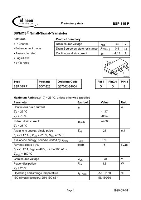
BSP 315 P SIPMOS® Small-Signal-Transistor
BSP 315 P SIPMOS® Small-Signal-Transistor
BSP 315 P SIPMOS® Small-Signal-Transistor

You also want an ePaper? Increase the reach of your titles
YUMPU automatically turns print PDFs into web optimized ePapers that Google loves.
Preliminary data<strong>BSP</strong> <strong>315</strong> PElectrical Characteristics, at T j = 25 °C, unless otherwise specifiedParameterSymbol Valuesmin. typ. max.UnitDynamic CharacteristicsGate to source chargeV DD = -48 V, I D = -1.17 AGate to drain chargeV DD = -48 V, I D = -1.17 AGate charge totalV DD = -48 V, I D = -1.17 A, V GS = 0 to -10 VGate plateau voltageV DD = -48 V, I D = -1.17 AQ gs-0.71.1Q gd - 1.8 2.6Q g-5.27.8V (plateau) - -3.14 - VnCParameter Symbol Values Unitmin. typ. max.Reverse DiodeInverse diode continuous forward current I S - - -1.17 AT A = 25 °CInverse diode direct current,pulsedI SM - - -4.68T A = 25 °CInverse diode forward voltageV SD - -0.97 -1.3 VV GS = 0 V, I F = -1.17 AReverse recovery timet rr - 30.5 46 nsV R = -30 V, I F =I S , di F /dt = 100 A/µsReverse recovery chargeV R = -30 V, I F =l S , di F /dt = 100 A/µsQ rr - 36 54 µCPage 41999-09-14
Preliminary data<strong>BSP</strong> <strong>315</strong> PTyp. output characteristicsI D = f (V DS )parameter: t p = 80 µsID-2.8A-2.4-2.2-2.0-1.8-1.6-1.4-1.2-1.0-0.8-0.6-0.4-0.2<strong>BSP</strong> <strong>315</strong> PP tot = 2Wlikjhg f eV GS[V]a -2.5db -3.0c -3.5d -4.0e -4.5f -5.0g -5.5ch -6.0i -6.5j -7.0k -8.0b l -10.0aTyp. drain-source-on-resistanceR DS(on) = f (I D )parameter: V GSRDS(on)2.6Ω2.22.01.81.61.41.21.00.80.60.40.2<strong>BSP</strong> <strong>315</strong> PaV GS [V] =a-2.5b-3.0c-3.5bd-4.0e-4.5f-5.0cg-5.5h-6.0i-6.5dj-7.0efgi hk jlk l-8.0 -10.00.00.0 -0.5 -1.0 -1.5 -2.0 -2.5 -3.0 -3.5 -4.0 V -5.0V DSTyp. transfer characteristics I D = f ( V GS )V DS ≥ 2 x I D x R DS(on)maxparameter: t p = 80 µs-3.00.00.0 -0.4 -0.8 -1.2 -1.6 -2.0 A -2.6I DTyp. forward transconductancegfs = f(I D ); T j =25°Cparameter: g fs2.5ASID-2.0g fs1.5-1.51.0-1.0-0.50.50.00.0 -1.0 -2.0 -3.0 -4.0 V -6.00.00.0 0.5 1.0 1.5 2.0 A 3.0V GSI DPage 61999-09-14
Preliminary data<strong>BSP</strong> <strong>315</strong> PDrain-source on-resistanceR DS(on) = f (T j )parameter:I D = -1.17 A, V GS = -10 V2.1Ω1.8<strong>BSP</strong> <strong>315</strong> PGate threshold voltageV GS(th) = f (T j )parameter: V GS = V DS , I D = -160 µA-3.0VRDS(on)1.61.41.21.098%VGS(th)-2.0-1.598%typ0.80.6typ-1.02%0.4-0.50.20.0-60 -20 20 60 100 °C 180T jTyp. capacitancesC = f(VDS)Parameter: V GS =0 V, f=1 MHz3100.0-60 -20 20 60 100 °C 160T jForward characteristics of reverse diodeI F = f (V SD )parameter: T j , tp = 80 µs1-10<strong>BSP</strong> <strong>315</strong> PpFA210C iss0-10CIFC ossC rss110-1-10T j = 25 °C typT j = 150 °C typT j = 25 °C (98%)T j = 150 °C (98%)0100 -5 -10 -15 -20 -25 -30 V -40V DSPage 7-2-100.0 -0.4 -0.8 -1.2 -1.6 -2.0 -2.4 V -3.0V SD1999-09-14
Preliminary data<strong>BSP</strong> <strong>315</strong> PAvalanche Energy E AS = f (T j )parameter: I D = -1.17 A , V DD = -25 VR GS = 25 Ω25Typ. gate chargeV GS = f (Q Gate )parameter: I D = -1.17 A pulsed<strong>BSP</strong> <strong>315</strong> P-16mJV-12EAS15VGS-10-810-60,2 VDS max0,8 VDS max5-4-2025 45 65 85 105 125 °C 165T j00.0 1.0 2.0 3.0 4.0 5.0 6.0 nC 8.0Q GateDrain-source breakdown voltageV (BR)DSS = f (T ) j-72<strong>BSP</strong> <strong>315</strong> PVV(BR)DSS-68-66-64-62-60-58-56-54-60 -20 20 60 100 °C 180T jPage 81999-09-14
Preliminary data<strong>BSP</strong> <strong>315</strong> PPublished byInfineon Technologies AG,Bereichs KommunikationSt.-Martin-Strasse 53,D-81541 München© Infineon Technologies AG 1999All Rights Reserved.Attention please!The information herein is given to describe certain components and shall not be considered as warrantedcharacteristics.Terms of delivery and rights to technical change reserved.We hereby disclaim any and all warranties, including but not limited to warranties of non-infringement,regarding circuits, descriptions and charts stated herein.Infineon Technologies is an approved CECC manufacturer.InformationFor further information on technology, delivery terms and conditions and prices please contact your nearestInfineon Technologies Office in Germany or our Infineon Technologies Reprensatives worldwide (see address list).WarningsDue to technical requirements components may contain dangerous substances.For information on the types in question please contact your nearest Infineon Technologies Office.Infineon Technologies Components may only be used in life-support devices or systems with the expresswritten approval of Infineon Technologies, if a failure of such components can reasonably be expected tocause the failure of that life-support device or system, or to affect the safety or effectiveness of that deviceor system Life support devices or systems are intended to be implanted in the human body, or to supportand/or maintain and sustain and/or protect human life. If they fail, it is reasonable to assume that the healthof the user or other persons may be endangered.Page 91999-09-14