N-CHANNEL 500V - 0.75 OHM - 8A - TO-220 POWERMESH MOSFET
N-CHANNEL 500V - 0.75 OHM - 8A - TO-220 POWERMESH MOSFET
N-CHANNEL 500V - 0.75 OHM - 8A - TO-220 POWERMESH MOSFET
- No tags were found...

You also want an ePaper? Increase the reach of your titles
YUMPU automatically turns print PDFs into web optimized ePapers that Google loves.
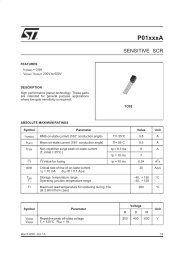
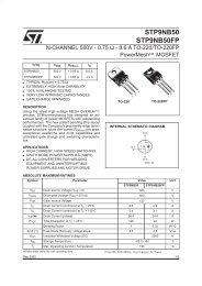
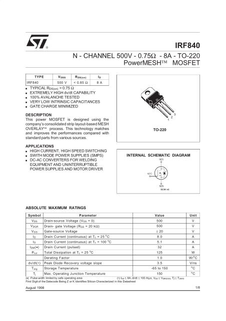
®IRF840N - <strong>CHANNEL</strong> <strong>500V</strong> - <strong>0.75</strong>Ω - <strong>8A</strong> - <strong>TO</strong>-<strong>220</strong>PowerMESH <strong>MOSFET</strong>TYPE V DSS R DS(on) I DIRF840 500 V < 0.85 Ω <strong>8A</strong>■■■■■TYPICAL R DS(on) = <strong>0.75</strong> ΩEXTREMELY HIGH dv/dt CAPABILITY100% AVALANCHE TESTEDVERY LOW INTRINSIC CAPACITANCESGATE CHARGE MINIMIZEDDESCRIPTIONThis power <strong>MOSFET</strong> is designed using thecompany’s consolidated strip layout-based MESHOVERLAY process. This technology matchesand improves the performances compared withstandard parts from various sources.APPLICATIONS■ HIGH CURRENT, HIGH SPEED SWITCHING■ SWITH MODE POWER SUPPLIES (SMPS)■ DC-AC CONVERTERS FOR WELDINGEQUIPMENT AND UNINTERRUPTIBLEPOWER SUPPLIES AND MO<strong>TO</strong>R DRIVER<strong>TO</strong>-<strong>220</strong>1 23INTERNAL SCHEMATIC DIAGRAMABSOLUTE MAXIMUM RATINGSSymbol Parameter Value UnitVDS Drain-source Voltage (VGS =0) 500 VV DGR Drain- gate Voltage (RGS =20kΩ) 500 VV GS Gate-source Voltage ± 20 VID Drain Current (continuous) at Tc =25 o C 8.0 AID Drain Current (continuous) at Tc =100 o C 5.1 AI DM (•) Drain Current (pulsed) 32 AP tot Total Dissipation at T c =25 o C 125 WDerating Factor 1.0 W/ o Cdv/dt(1) Peak Diode Recovery voltage slope 3.5 V/nsT stg Storage Temperature -65 to 150T j Max. Operating Junction Temperature 150(•) Pulse width limited by safe operating area(1) I SD ≤ <strong>8A</strong>, di/dt ≤ 100 A/µs, V DD ≤ V (BR)DSS, Tj≤T JMAXFirst Digit of the Datecode Being Z or K Identifies Silicon Characterized in this DatasheetAugust 1998o Co C1/8
IRF840ELECTRICAL CHARACTERISTICS (continued)SWITCHING ONSymbol Parameter Test Conditions Min. Typ. Max. Unittd(on)t rQgQ gsQgdTurn-on TimeRise TimeTotal Gate ChargeGate-Source ChargeGate-Drain ChargeVDD =250V ID=4.3ARG=4.7 Ω VGS =10V(see test circuit, figure 3)1911VDD =400V ID=8.0A VGS =10V 3910.613.7nsns50 nCnCnCSWITCHING OFFSymbol Parameter Test Conditions Min. Typ. Max. Unitt r(Voff)tft cOff-voltage Rise TimeFall TimeCross-over TimeV DD =400V I D =<strong>8A</strong>R G =4.7 Ω V GS =10V(see test circuit, figure 5)11.51120nsnsnsSOURCE DRAIN DIODESymbol Parameter Test Conditions Min. Typ. Max. UnitI SDI SDM (•)Source-drain CurrentSource-drain Current(pulsed)VSD (∗) Forward On Voltage ISD =8.0A VGS =0 1.6 Vtrr Reverse Recovery I SD = 8.0 A di/dt = 100 A/µs420nsTimeVDD =100V Tj=150 o CQrrIRRMReverse RecoveryChargeReverse Recovery(see test circuit, figure 5)3.516.5µCACurrent(∗) Pulsed: Pulse duration = 300 µs, duty cycle 1.5 %(•) Pulse width limited by safe operating area8.032AASafe Operating AreaThermal Impedance3/8
IRF840Output CharacteristicsTransfer CharacteristicsTransconductanceStatic Drain-source On ResistanceGate Charge vs Gate-source VoltageCapacitance Variations4/8
IRF840Normalized Gate Threshold Voltage vsTemperatureNormalized On Resistance vs TemperatureSource-drain Diode Forward Characteristics5/8
IRF840Fig. 1: Unclamped Inductive Load Test CircuitFig. 1: Unclamped Inductive WaveformFig. 3: Switching Times Test Circuits ForResistive LoadFig. 4: Gate Charge test CircuitFig. 5: Test Circuit For Inductive Load SwitchingAnd Diode Recovery Times6/8
IRF840<strong>TO</strong>-<strong>220</strong> MECHANICAL DATADIM.mminchMIN. TYP. MAX. MIN. TYP. MAX.A 4.40 4.60 0.173 0.181C 1.23 1.32 0.048 0.051D 2.40 2.72 0.094 0.107D1 1.27 0.050E 0.49 0.70 0.019 0.027F 0.61 0.88 0.024 0.034F1 1.14 1.70 0.044 0.067F2 1.14 1.70 0.044 0.067G 4.95 5.15 0.194 0.203G1 2.4 2.7 0.094 0.106H2 10.0 10.40 0.393 0.409L2 16.4 0.645L4 13.0 14.0 0.511 0.551L5 2.65 2.95 0.104 0.116L6 15.25 15.75 0.600 0.620L7 6.2 6.6 0.244 0.260L9 3.5 3.93 0.137 0.154DIA. 3.75 3.85 0.147 0.151GD1CDAEL2G1H2F1Dia.FL5L7L9F2L6L4P011C7/8
IRF840Information furnished is believed to be accurate and reliable. However, STMicroelectronics assumes no responsibility for the consequencesof use of such information nor for any infringement of patents or other rights of third parties which may result from its use. No license isgranted by implication or otherwise under any patent or patent rights of STMicroelectronics. Specification mentioned in this publication aresubject to change without notice. This publication supersedes and replaces all information previously supplied. STMicroelectronics productsare not authorized for use as critical components in life support devices or systems without express written approval of STMicroelectronics.The ST logo is a registered trademark of STMicroelectronics© 1998 STMicroelectronics – Printed in Italy – All Rights ReservedSTMicroelectronics GROUP OF COMPANIESAustralia - Brazil - Canada - China - France - Germany - Italy - Japan - Korea - Malaysia - Malta - Mexico - Morocco - The Netherlands -Singapore - Spain - Sweden - Switzerland - Taiwan - Thailand - United Kingdom - U.S.A..8/8