EUROPEAN WHITE BOOK
EUROPEAN WHITE BOOK
EUROPEAN WHITE BOOK

Create successful ePaper yourself
Turn your PDF publications into a flip-book with our unique Google optimized e-Paper software.
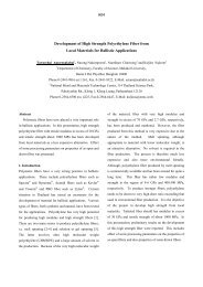
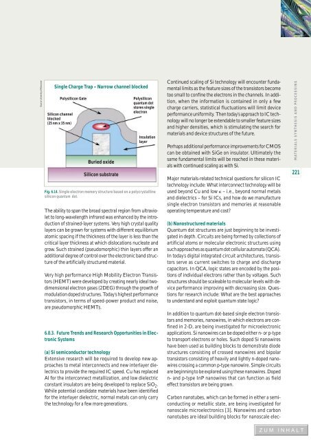
Source: University of WisconsinSingle Charge Trap – Narrow channel blockedSilicon channelblocked(25 nm x 35 nm)Polysilicon GateBuried oxideSilicon substratePolysiliconquantum dotstores singleelectronInsulationlayerFig. 6.14. Single electron memory structure based on a polycrystallinesilicon quantum dot.The ability to span the broad spectral region from ultravioletto long-wavelength infrared was enhanced by the introductionof strained-layer systems. Very high crystal qualitylayers can be grown for systems with different equilibriumatomic spacing if the thickness of the layer is less than thecritical layer thickness at which dislocations nucleate andgrow. Such strained (pseudomorphic) thin layers offer anadditional degree of control over the electronic band structureof the artificially structured material.Very high performance High Mobility Electron Transistors(HEMT) were developed by creating nearly ideal twodimensionalelectron gases (2DEG) through the growth ofmodulation doped structures. Today’s highest performancetransistors, in terms of speed-power product and noise,are pseudomorphic HEMTs.6.8.3. Future Trends and Research Opportunities in ElectronicSystems(a) Si semiconductor technologyExtensive research will be required to develop new approachesto metal interconnects and new interlayer dielectricsto provide the required IC speed. Cu has replacedAl for the interconnect metallization, and low dielectricconstant insulators are being developed to replace SiO 2 .While potential candidate materials have been identifiedfor the interlayer dielectric, normal metals can only carrythe technology for a few more generations.Continued scaling of Si technology will encounter fundamentallimits as the feature sizes of the transistors becometoo small to confine the electrons in the channels. In addition,when the information is contained in only a fewcharge carriers, statistical fluctuations will limit deviceperformance uniformity. Then today’s approach to IC technologywill no longer be extendable to smaller feature sizesand higher densities, which is stimulating the search formaterials and device structures of the future.Perhaps additional performance improvements for CMOScan be obtained with SiGe on insulator. Ultimately thesame fundamental limits will be reached in these materialswith continued scaling as with Si.Major materials-related technical questions for silicon ICtechnology include: What interconnect technology will beused beyond Cu and low – i.e., beyond normal metalsand dielectrics – for Si ICs, and how do we manufacturesingle electron transistors and memories at reasonableoperating temperature and cost?(b) Nanostructured materialsQuantum dot structures are just beginning to be investigatedin depth. Circuits are being formed by collections ofartificial atoms or molecular electronic structures usingsuch approaches as quantum dot cellular automata (QCA).In today’s digital integrated circuit architectures, transistorsserve as current switches to charge and dischargecapacitors. In QCA, logic states are encoded by the positionsof individual electrons rather than by voltages. Suchstructures should be scaleable to molecular levels with deviceperformance improving with decreasing size. Questionsfor research include: What are the best approachesto understand and exploit quantum state logic?In addition to quantum dot-based single electron transistorsand memories, nanowires, in which electrons are confinedin 2-D, are being investigated for microelectronicapplications. Si nanowires can be doped either n- or p-typeto transport electrons or holes. Such doped Si nanowireshave been used as building blocks to demonstrate diodestructures consisting of crossed nanowires and bipolartransistors consisting of heavily and lightly n-doped nanowirescrossing a common p-type nanowire. Simple circuitsare beginning to be explored using these nanowires. Dopedn- and p-type InP nanowires that can function as fieldeffect transistors are being grown.Carbon nanotubes, which can be formed in either a semiconductingor metallic state, are being investigated fornanoscale microelectronics [3]. Nanowires and carbonnanotubes are ideal building blocks for nanoscale elec-MATERIALS SYNTHESIS AND PROCESSING221