EUROPEAN WHITE BOOK
EUROPEAN WHITE BOOK
EUROPEAN WHITE BOOK

Create successful ePaper yourself
Turn your PDF publications into a flip-book with our unique Google optimized e-Paper software.
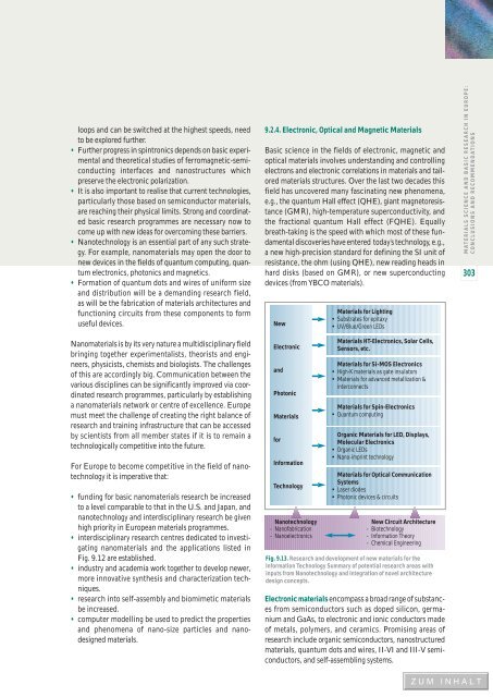
loops and can be switched at the highest speeds, needto be explored further.• Further progress in spintronics depends on basic experimentaland theoretical studies of ferromagnetic-semiconductinginterfaces and nanostructures whichpreserve the electronic polarization.• It is also important to realise that current technologies,particularly those based on semiconductor materials,are reaching their physical limits. Strong and coordinatedbasic research programmes are necessary now tocome up with new ideas for overcoming these barriers.• Nanotechnology is an essential part of any such strategy.For example, nanomaterials may open the door tonew devices in the fields of quantum computing, quantumelectronics, photonics and magnetics.• Formation of quantum dots and wires of uniform sizeand distribution will be a demanding research field,as will be the fabrication of materials architectures andfunctioning circuits from these components to formuseful devices.Nanomaterials is by its very nature a multidisciplinary fieldbringing together experimentalists, theorists and engineers,physicists, chemists and biologists. The challengesof this are accordingly big. Communication between thevarious disciplines can be significantly improved via coordinatedresearch programmes, particularly by establishinga nanomaterials network or centre of excellence. Europemust meet the challenge of creating the right balance ofresearch and training infrastructure that can be accessedby scientists from all member states if it is to remain atechnologically competitive into the future.For Europe to become competitive in the field of nanotechnologyit is imperative that:• funding for basic nanomaterials research be increasedto a level comparable to that in the U.S. and Japan, andnanotechnology and interdisciplinary research be givenhigh priority in European materials programmes.• interdisciplinary research centres dedicated to investigatingnanomaterials and the applications listed inFig. 9.12 are established.• industry and academia work together to develop newer,more innovative synthesis and characterization techniques.• research into self-assembly and biomimetic materialsbe increased.• computer modelling be used to predict the propertiesand phenomena of nano-size particles and nanodesignedmaterials.9.2.4. Electronic, Optical and Magnetic MaterialsBasic science in the fields of electronic, magnetic andoptical materials involves understanding and controllingelectrons and electronic correlations in materials and tailoredmaterials structures. Over the last two decades thisfield has uncovered many fascinating new phenomena,e.g., the quantum Hall effect (QHE), giant magnetoresistance(GMR), high-temperature superconductivity, andthe fractional quantum Hall effect (FQHE). Equallybreath-taking is the speed with which most of these fundamentaldiscoveries have entered today’s technology, e.g.,a new high-precision standard for defining the SI unit ofresistance, the ohm (using QHE), new reading heads inhard disks (based on GMR), or new superconductingdevices (from YBCO materials).NewElectronicandPhotonicMaterialsforInformationTechnologyNanotechnology- Nanofabrication- NanoelectronicsMaterials for Lighting• Substrates for epitaxy• UV/Blue/Green LEDsMaterials HT-Electronics, Solar Cells,Sensors, etc.Materials for Si-MOS Electronics• High-K materials as gate insulators• Materials for advanced metallization &interconnectsMaterials for Spin-Electronics• Quantum computingOrganic Materials for LED, Displays,Molecular Electronics• Organic LEDs• Nano-imprint technologyMaterials for Optical CommunicationSystems• Laser diodes• Photonic devices & circuitsNew Circuit Architecture- Biotechnology- Information Theory- Chemical EngineeringFig. 9.13. Research and development of new materials for theInformation Technology Summary of potential research areas withinputs from Nanotechnology and integration of novel architecturedesign concepts.Electronic materials encompass a broad range of substancesfrom semiconductors such as doped silicon, germaniumand GaAs, to electronic and ionic conductors madeof metals, polymers, and ceramics. Promising areas ofresearch include organic semiconductors, nanostructuredmaterials, quantum dots and wires, II-VI and III-V semiconductors,and self-assembling systems.MATERIALS SCIENCE AND BASIC RESEARCH IN EUROPE:CONCLUSIONS AND RECOMMENDATIONS303