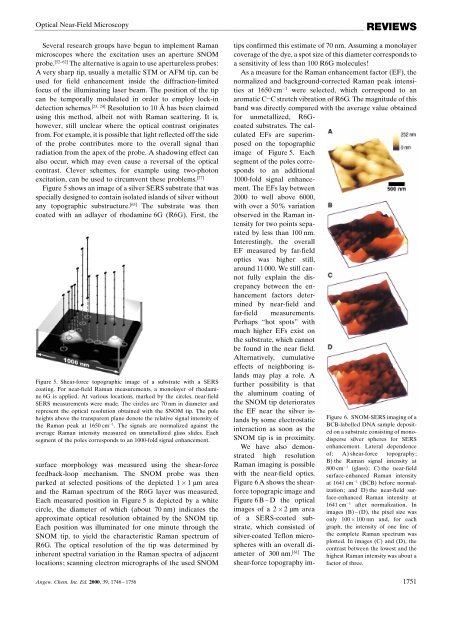
<strong>Optical</strong> <strong>Near</strong>-<strong>Field</strong> <strong>Microscopy</strong>Several research groups have begun to implement Ramanmicroscopes where the excitation uses an aperture SNOMprobe. [52±62] The alternative is again to use apertureless probes:A very sharp tip, usually a metallic STM or AFM tip, can beused for field enhancement inside the diffraction-limitedfocus of the illuminating l<strong>as</strong>er beam. The position of the tipcan be temporally modulated in order to employ lock-indetection schemes. [23, 24] Resolution to 10 Š h<strong>as</strong> been claimedusing this method, albeit not with Raman scattering. It is,however, still unclear where the optical contr<strong>as</strong>t originatesfrom. For example, it is possible that light reflected off the sideof the probe contributes more to the overall signal thanradiation from the apex of the probe. A shadowing effect canalso occur, which may even cause a reversal of the opticalcontr<strong>as</strong>t. Clever schemes, for example using two-photonexcitation, can be used to circumvent these problems. [27]Figure 5 shows an image of a silver SERS substrate that w<strong>as</strong>specially designed to contain isolated isl<strong>and</strong>s of silver withoutany topographic substructure. [63] The substrate w<strong>as</strong> thencoated with an adlayer of rhodamine 6G (R6G). First, theFigure 5. Shear-force topographic image of a substrate with a SERScoating. For near-field Raman me<strong>as</strong>urements, a monolayer of rhodamine6G is applied. At various locations, marked by the circles, near-fieldSERS me<strong>as</strong>urements were made. The circles are 70 nm in diameter <strong>and</strong>represent the optical resolution obtained with the SNOM tip. The poleheights above the transparent plane denote the relative signal intensity ofthe Raman peak at 1650 cm 1 . The signals are normalized against theaverage Raman intensity me<strong>as</strong>ured on unmetallized gl<strong>as</strong>s slides. Eachsegment of the poles corresponds to an 1000-fold signal enhancement.surface morphology w<strong>as</strong> me<strong>as</strong>ured using the shear-forcefeedback-loop mechanism. The SNOM probe w<strong>as</strong> thenparked at selected positions of the depicted 1 1 mm area<strong>and</strong> the Raman spectrum of the R6G layer w<strong>as</strong> me<strong>as</strong>ured.Each me<strong>as</strong>ured position in Figure 5 is depicted by a whitecircle, the diameter of which (about 70 nm) indicates theapproximate optical resolution obtained by the SNOM tip.Each position w<strong>as</strong> illuminated for one minute through theSNOM tip, to yield the characteristic Raman spectrum ofR6G. The optical resolution of the tip w<strong>as</strong> determined byinherent spectral variation in the Raman spectra of adjacentlocations; scanning electron micrographs of the used SNOMREVIEWStips confirmed this estimate of 70 nm. Assuming a monolayercoverage of the dye, a spot size of this diameter corresponds toa sensitivity of less than 100 R6G molecules!As a me<strong>as</strong>ure for the Raman enhancement factor (EF), thenormalized <strong>and</strong> background-corrected Raman peak intensitiesat 1650 cm 1 were selected, which correspond to anaromatic C C stretch vibration of R6G. The magnitude of thisb<strong>and</strong> w<strong>as</strong> directly compared with the average value obtainedfor unmetallized, R6Gcoatedsubstrates. The calculatedEFs are superimposedon the topographicimage of Figure 5. Eachsegment of the poles correspondsto an additional1000-fold signal enhancement.The EFs lay between2000 to well above 6000,with over a 50 % variationobserved in the Raman intensityfor two points separatedby less than 100 nm.Interestingly, the overallEF me<strong>as</strong>ured by far-fieldoptics w<strong>as</strong> higher still,around 11 000. We still cannotfully explain the discrepancybetween the enhancementfactors determinedby near-field <strong>and</strong>far-field me<strong>as</strong>urements.Perhaps ªhot spotsº withmuch higher EFs exist onthe substrate, which cannotbe found in the near field.Alternatively, cumulativeeffects of neighboring isl<strong>and</strong>smay play a role. Afurther possibility is thatthe aluminum coating ofthe SNOM tip deterioratesthe EF near the silver isl<strong>and</strong>sby some electrostaticinteraction <strong>as</strong> soon <strong>as</strong> theSNOM tip is in proximity.We have also demonstratedhigh resolutionRaman imaging is possiblewith the near-field optics.Figure 6 A shows the shearforcetopograpic image <strong>and</strong>Figure 6 B ± D the opticalimages of a 2 2 mm areaof a SERS-coated substrate,which consisted ofsilver-coated Teflon microsphereswith an overall diameterof 300 nm. [61] Theshear-force topography im-Figure 6. SNOM-SERS imaging of aBCB-labelled DNA sample depositedon a substrate consisting of monodispersesilver spheres for SERSenhancement. Lateral dependenceof: A) shear-force topography;B) the Raman signal intensity at800 cm 1 (gl<strong>as</strong>s); C) the near-fieldsurface-enhanced Raman intensityat 1641 cm 1 (BCB) before normalization;<strong>and</strong> D) the near-field surface-enhancedRaman intensity at1641 cm 1 after normalization. Inimages (B) ± (D), the pixel size w<strong>as</strong>only 100 100 nm <strong>and</strong>, for eachgraph, the intensity of one line ofthe complete Raman spectrum w<strong>as</strong>plotted. In images (C) <strong>and</strong> (D), thecontr<strong>as</strong>t between the lowest <strong>and</strong> thehighest Raman intensity w<strong>as</strong> about afactor of three.Angew. Chem. Int. Ed. 2000, 39, 1746 ± 1756 1751
REVIEWSage shows that aggregated silver spheres are clearly resolved<strong>and</strong> their spatial distribution is quite irregular. This substratew<strong>as</strong> coated with a monolayer of a 18-mer DNA fragmentlabelled with brilliant cresyl blue (BCB). [62] To achieve are<strong>as</strong>onable acquisition time for the entire image, we me<strong>as</strong>uredthe near-field Raman spectra <strong>as</strong> an array of only 20 20 datapoints. This acquisition time w<strong>as</strong> twenty times longer comparedto normal SNOM imaging times. Nevertheless, for anaperture smaller than 100 nm, it is the tip size <strong>and</strong> not the stepsize that limits the optical resolution. This represents a slightundersampling that we accept in order to obtain the entirespectral information within a re<strong>as</strong>onable me<strong>as</strong>urement time.The image of the Raman spectrum feature at 800 cm 1(Figure 6 B), which stems from the gl<strong>as</strong>s of the SNOM tipitself, is at le<strong>as</strong>t partially dependent upon the topography.From the comparison of Figures 6 A <strong>and</strong> B, it is obvious thatthe correlation of the topographic information <strong>and</strong> thereflected light from such a highly corrugated sample is byno means trivial. In particular, an interpretation of the image<strong>and</strong> an estimation of the optical resolution is difficult iftopographic coupling or shadowing effects [20] occur.The image in Figure 6 C shows the lateral intensity dependenceof the Raman b<strong>and</strong> from the BCB label (at 1641 cm 1 ).By comparing Figures 6 B <strong>and</strong> 6 C, it is apparent that Ramansignals from the label <strong>and</strong> from the gl<strong>as</strong>s tip show somecorrelation, such <strong>as</strong> the incre<strong>as</strong>ed intensity in the lower leftcorner. However, the Raman signal stems from the BCBlabelledDNA, where<strong>as</strong> the gl<strong>as</strong>s scattering signal originatesentirely from the SNOM tip. The b<strong>and</strong>s from the gl<strong>as</strong>stherefore should be proportional to the local reflectivity of thesurface. The Raman scattered signal is subject to the samereflectivity changes <strong>as</strong> the gl<strong>as</strong>s signal. If, for instance, aparticle between the illuminated spot <strong>and</strong> the collection opticsdecre<strong>as</strong>es the reflectivity, the Raman signal is attenuated inexactly the same f<strong>as</strong>hion <strong>and</strong> extent. In other words, thetopography of our sample is encoded in the reflectivity signal,such that the topographic effects can be removed from theRaman signal by normalizing it against the intensity of thegl<strong>as</strong>s b<strong>and</strong>. The effect of this normalization is demonstrated inFigure 6 D, in which the Raman intensity of the 1641 cm 1BCB b<strong>and</strong> at each position after dividing the data inFigure 6 C by the intensity of Figure 6 B. A comparison ofFigures 6 D <strong>and</strong> 6 C shows that instead of two bright spots, thecorrected image shows only one spot of high SERS intensity.At the position in the lower left, an enhanced samplereflectivity is responsible for the incre<strong>as</strong>ed Raman signal,where<strong>as</strong> the bright spot on the upper left remains after thenormalization.In the corrected Raman images at all frequencies, weobserve a small, highly SERS-active region of about 400 nmdiameter on the center-left side of the image. If we <strong>as</strong>sume auniform distribution of the sample on the surface, thisincre<strong>as</strong>e in intensity can only be attributed to a particularlystrong enhancement by the substrate (ªhot spotsº), althoughconcentration fluctuations leading to a variation of Ramansignals cannot entirely be excluded. Interestingly, the maximumSERS enhancement does not coincide with the positionof a silver particle but, in fact, the location of the maximumenhancement seems to be at a position where a gap betweenR. Zenobi <strong>and</strong> V. DeckertFigure 7. Raman lines superimposedon a fluorescencebackground in the optical spectrumof a monolayer of rhodamine6G deposited on a silverSERS substrate (excitation at488 nm). The spectra were recordedconsecutively (from topto bottom), using an integrationtime of 5 min per spectrum.Slow photobleaching isobserved for the fluorescencebackground, while the intensityof the Raman lines remainsconstant.the silver spheres is visible (Figure 6 A). We have to be awareof the possibility that the topographic <strong>and</strong> the SNOM-Ramanimage may not be in perfect congruence. It h<strong>as</strong> beenpostulated that ªhot spotsº may be located on SERSsubstrates where gaps or cavities exist. [64] In previous workby Emory <strong>and</strong> Nie, [56] there are hints for such ªhot spotsº butthey were unable to image these sites directly. In contr<strong>as</strong>t, theSNOM method allows directly visualization of ªhot spotsºbecause of the simultaneousrecording of sample topography<strong>and</strong> Raman intensity at eachdata point; this is particularlystraightforward if low-densitysilver-isl<strong>and</strong> films are used <strong>as</strong>SERS substrates. [63]It is interesting to comparethe relative magnitude of Ramanscattered light <strong>and</strong> fluorescencesignals. The cross sectionsfound for SERS on ªhot spotsºw<strong>as</strong> of the same order of magnitude<strong>as</strong> that of the fluorescencesignals! Upon[56, 65]absorptionof a single photon, anindividual molecule will eitherundergo a Raman scatteringevent or fluoresce, but not both.Photobleaching processes areintimately linked with fluorescence<strong>and</strong> therefore should notaffect the Raman emissionprocess. This is demonstratedin Figure 7, where three consecutivespectra of R6G depositedon a silver-isl<strong>and</strong> SERS substrateare shown. The intensityof the fluorescence backgrounddecre<strong>as</strong>es due to photobleaching,while that of the Ramanb<strong>and</strong>s remains constant, inagreement with the expectation.The re<strong>as</strong>on for this behaviormay be that ªhot spotsº on the SERS substrate coax theadsorbed molecules into undergoing Raman scattering ratherthan fluorescence, thereby protecting them from photobleaching.The average coverage of the SERS substrate bythe dye w<strong>as</strong> slightly more than one monolayer; apparentlyonly a fraction of the adsorbed R6G molecules are <strong>as</strong>sociatedwith these protective sites but are responsible for quite strongSERS signals. This again supports the idea that only a fewªhot spotsº exhibit a very large Raman enhancement <strong>and</strong> areresponsible for the overall intensity observed.Are SERS methods the only hope to obtain Raman spectraexcited by near-field optical probes? The answer to thisquestion is, <strong>as</strong> demonstrated in Figure 8, a clear ªnoº. Thenear-field Raman spectrum of a chemical-vapor deposited(CVD) diamond film shows a sharp feature at 1330 cm 1 ,which is the well known Raman b<strong>and</strong> of diamond. Ramanscattering from graphitic carbon is expected around1752 Angew. Chem. Int. Ed. 2000, 39, 1746 ± 1756