Scanning Near-Field Optical Microscopy and Spectroscopy as a ...
Scanning Near-Field Optical Microscopy and Spectroscopy as a ...
Scanning Near-Field Optical Microscopy and Spectroscopy as a ...

You also want an ePaper? Increase the reach of your titles
YUMPU automatically turns print PDFs into web optimized ePapers that Google loves.
REVIEWS<strong>Scanning</strong> <strong>Near</strong>-<strong>Field</strong> <strong>Optical</strong> <strong>Microscopy</strong> <strong>and</strong> <strong>Spectroscopy</strong> <strong>as</strong> a Tool forChemical AnalysisRenato Zenobi* <strong>and</strong> Volker DeckertResearch into the nanometer-scale regionis currently of relevance in manybranches of modern science <strong>and</strong> engineering,such <strong>as</strong> in microelectronics,supramolecular chemistry, <strong>and</strong> in abiological context. A great deal ofattention is given to the design ofmolecular devices, usually towards underst<strong>and</strong>ingthe function of existingªmolecular machinesº. Central to thist<strong>as</strong>k are powerful diagnostic tools capableof recording chemical informationwith spatial resolution in thenanometer range. While elementalanalysis of surfaces with a lateralresolution of a few dozen nanometersis almost routine, analysis of molecularspecies with a resolution of < 1 mm isvery difficult. <strong>Scanning</strong>-tunneling <strong>and</strong>atomic-force microscopies usually donot give any chemical information. Bycombining scanning near-field opticalmicroscopy (SNOM)Ðthe ªopticalmemberº of the family of scanningprobemicroscopiesÐwith opticalspectroscopy, it is possible to obtainmolecular information from sampleare<strong>as</strong> <strong>as</strong> little <strong>as</strong> 50 nm in diameter. InSNOM, a light source is scanned abovethe object of interest at a distance of afew nanometers. In the optical nearfield, the illuminated area is not subjectto the Abbe diffraction limit, butmerely by the size of the illuminatingsource. High quality SNOM probes canbe reproducibly prepared by a chemical-etchingmethod. These etchedprobes have an optical transmissionup to 1000-fold higher than commercial(pulled) SNOM tips <strong>and</strong> can withst<strong>and</strong>higher l<strong>as</strong>er power. This l<strong>as</strong>tadvantage allows not only high resolutionoptical imaging, but also localizedspectroscopic investigations ofsurfaces <strong>and</strong> even optical ªnanosamplingºby pulsed-l<strong>as</strong>er ablation. Theablated material can be transportedover a considerable distance, whichopens the possibility for its subsequentanalysis with a complementary, highlysensitive analytical method, such <strong>as</strong>m<strong>as</strong>s spectrometry.Keywords: analytical methods ´ m<strong>as</strong>sspectrometry ´ optical near-field microscopy´ optical spectroscopy ´ surfaceanalysis1. IntroductionA great breakthrough in surface science w<strong>as</strong> the developmentof the scanning-probe microscopy techniques, led by thedevelopment of the scanning-tunneling microscope (STM),which earned Heinrich Rohrer <strong>and</strong> Gerd Binnig the 1986Nobel Prize in Physics. [1±3] Soon thereafter, a host of relatedmethods were developed, all b<strong>as</strong>ed on piezoelectric scanningof a very sharp probe relative to the sample, such <strong>as</strong> atomicforcemicroscopy (AFM), scanning electrochemical microscopy,scanning magnetic microscopy, <strong>and</strong> many others. Theyare sometimes collectively referred to <strong>as</strong> the ªchildren of theSTMº. [4][*] Prof. R. Zenobi, Dr. V. DeckertLaboratorium für Organische ChemieEidgenössische Technische Hochschule (ETH) ZürichUniversitätsstr<strong>as</strong>se 16, 8092 Zürich (Switzerl<strong>and</strong>)Fax: (‡ 41) 1-632-12-92E-mail: zenobi@org.chem.ethz.chOf particular interest to applications in molecular science isscanning near-field optical microscopy (SNOM), [5±8] theªopticalº version among the children of the STM. SNOMdelivers light to spots of less than 100 nm diameter <strong>and</strong>thereby holds great promise for molecular analysis on thenanometer scale. An optical resolution of <strong>as</strong> little <strong>as</strong> 12 nm h<strong>as</strong>been claimed by Betzig <strong>and</strong> Trautman [9] but only afterdeconvolution of the size of the near-field optical probe. Thisspatial resolution h<strong>as</strong> not been reproduced lately by otherresearchers. Delivering light to such small spots is not possibleby conventional optical methods, such <strong>as</strong> by a focussed l<strong>as</strong>erbeam. It is also impossible to resolve features separated byless than l/2 by conventional optical microscopy, where l isthe wavelength of the illuminating light. This limitation isimposed by the Abbe diffraction limit. At visible wavelengths,a resolution approaching 200 ± 250 nm should be theoreticallypossible but, except for confocal schemes employing oilimmersionlenses <strong>and</strong> therefore subject to other limitations, aresolution better than 0.5 ± 1 mm is rarely achieved. Thisdiffraction limit is the re<strong>as</strong>on that short-wavelength ultra-Angew. Chem. Int. Ed. 2000, 39, 1746 ± 1756 WILEY-VCHVerlag GmbH, D-69451 Weinheim, 2000 1433-7851/00/3910-1747 $ 17.50+.50/0 1747
REVIEWSviolet light or even X-rays, where l is smaller still, findincre<strong>as</strong>ing use in microelectronics <strong>and</strong> other applications oflithography but at the cost of more expensive optics <strong>and</strong>instrumentation.The possibility of illumination in the visible, in the nearultraviolet, or in the infrared range onto a spot smaller thanthe diffraction limit permits the application of a wide range ofspectroscopic methods to problems in chemistry, biology,materials science, <strong>and</strong> other fields in which the molecularcomposition of nanoscale objects is of interest. Analyzing theelemental composition with a resolution less than 100 nm isnow established <strong>and</strong> a routine procedure with scanning Augermicroscopy, some secondary-ion m<strong>as</strong>s spectrometers, <strong>and</strong>certain forms of electron-microprobe analysis. [10] These methodstypically operate under ultrahigh vacuum conditions,often require special sample pretreatment, <strong>and</strong> rely onfocussing an ion or electron beam to a spot
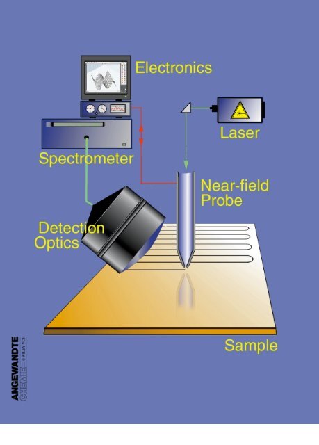
<strong>Optical</strong> <strong>Near</strong>-<strong>Field</strong> <strong>Microscopy</strong>Collected light is then filtered <strong>and</strong> projected onto a sensitivedetector for fluorescence detection or, alternatively, onto theentrance slit of an optical spectrograph. The latter isoptimized for a greater amount of transmitted light. In ourarrangement, a transmission holographic-grating spectrographwith a high numerical aperture w<strong>as</strong> used (Holospecf/1.8i, Kaiser <strong>Optical</strong> Systems, Ann Arbor, MI (USA)).To maintain a constant tip-to-sample distance, an opticallydetected shear-force feedback loop is most frequentlyused, [11, 12] although other methods have been employed. [13±17]For the feedback loop, the tip dithers at its resonancefrequency. The dithering amplitude decre<strong>as</strong>es dramaticallywhen the tip is within 5 ± 15 nm of the sample surface. There<strong>as</strong>ons for the shear force damping near the surface are stillnot fully understood; probably a combination of contact,frictional, <strong>and</strong> adhesive forces induced by a thin water film onthe sample surface are responsible, at le<strong>as</strong>t under ambientconditions. [18, 19] In the ªconstant gapº mode, a feedback loopmaintains a constant distance, normally < 10 nm, between theprobe <strong>and</strong> surface. For flat samples, scans in ªconstant heightmodeº are advantageous to avoid topographic artifacts. [20]Such scans are performed in the absence of a distancefeedback loop once the tip ± sample distance h<strong>as</strong> beenestablished.The probe is the most delicate component of any SNOMequipment. In this review, we will be dealing exclusively withªaperture SNOM probesº, that is, tips with an apex smallerthan the wavelength of the illuminating light, <strong>and</strong> made of a[12, 21]tapered gl<strong>as</strong>s fiber coated with metal except at the apex.Other probes are also used, including point-source emissionprobes [22] or apertureless probes. [23±28] The important propertiesof aperture SNOM probes are good transparency, a welldefined circular aperture, no light leaking through defects inthe metal coating, <strong>and</strong> a high optical-damage threshold.Several methods have been proposed to prepare the taperedgl<strong>as</strong>s core probes. Adiabatic pulling of optical fibers duringheating with a CO 2 l<strong>as</strong>er, [29, 30] similar to preparing a pipette, iscurrently the most popular method. In another c<strong>as</strong>e, tiny[31, 32]splinters of gl<strong>as</strong>s <strong>as</strong> tetrahedral SNOM tips are used.Several groups are employing focused ion-beam milling to[33, 34]create very well defined apertures at the tip apex.Recently, microfabricated tips have been described in theliterature [35±38] <strong>and</strong> such tips will become commerciallyavailable soon.A very practical method for the preparation of probes isb<strong>as</strong>ed on etching gl<strong>as</strong>s fibers at the meniscus betweenhydrofluoric acid (etching fluid) <strong>and</strong> a protective organicoverlayer. [39] Etched fiber probes usually provide a higheroptical throughput due to larger cone angles than the pulledprobes, [38±42] but a high yield of good tips produced by etchingis often not obtained. A more reproducible <strong>and</strong> efficientmethod, called ªtube etchingº, w<strong>as</strong> recently developed in ourlaboratory. [43] By this method, the protective polymer coatingof the optical fiber is retained, <strong>and</strong> a tip forms due to aconvective mechanism inside the polymer jacket. The methodis tolerant to perturbations during preparation such <strong>as</strong>vibrations <strong>and</strong> temperature changes. The resulting tips areproduced reproducibly <strong>and</strong> in high yield with large coneangles <strong>and</strong> smooth aluminum coating. It should also be notedREVIEWSthat the composition of the gl<strong>as</strong>s is crucial for obtaining goodetching results <strong>and</strong> also to avoid large background signalsduring SNOM experiments arising, for example, by Ramanscattering of the fiber material itself (see Section 3.2).The left side of Figure 2 shows an electron micrograph of analuminum-coated SNOM tip produced by the tube-etchingmethod. The large opening angle is immediately apparentFigure 2. Left: Electron micrograph of a SNOM tip produced by the tubeetchingmethod <strong>and</strong> a closeup of the apex region of the same tip.Right: Representation of the origin of differences between optical <strong>and</strong>topographic images.<strong>and</strong>, in the closeup, an aperture of well below 100 nmdiameter is visible. On the right side, the difference betweenthe ªtopographic tipº <strong>and</strong> the ªoptical tipº is illustrated.Sometimes a grain of the metal coating will protrude such thatthe center of the tapered optical fiber <strong>and</strong> that of thetopographic tip can be separated by several tens of nanometers.If this is the c<strong>as</strong>e, the offset of the topographic <strong>and</strong> theoptical images can lead to a misinterpretation of the combinedSNOM <strong>and</strong> topographic data.3. Results <strong>and</strong> Discussion3.1. Fluorescence Imaging with Etched <strong>Optical</strong>-Fiber TipsFluorescence is by far the most widespread <strong>and</strong> e<strong>as</strong>ilyimplemented mode for chemical imaging by near-field opticalmethods, although the resolution offered by modern confocalfluorescence-microscopy techniques is often sufficient. [44] Afluorescent tag must be attached to the molecules of interest,unless their natural fluorescence can be exploited. Due tohigh signal intensity, it is even possible to image singlefluorescent molecules with SNOM technology. F<strong>as</strong>cinatingapplications, involving single molecule fluorescence detection,have been described by Betzig, [45] Xie, [46±48] <strong>and</strong> vanHulst. [49]A very promising area for the use of SNOM in combinationwith fluorescence detection is the study of biological nanostructures,in particular, parts of cells. An example from ourlaboratory is shown in Figure 3 A. In this application, dogkidney (Madine ± Darby canine kidney, MDCK) cells weregrown on a flat silica slide using glutaraldehyde <strong>and</strong> lysed suchthat the interior of their cell walls became accessible toSNOM imaging. [50] The actin filaments of the cytoskeletonwere stained selectively with a rhodamine-labeled phalloidin;they appear green in the image.Figure 3 shows immediately that much finer features areresolved with SNOM. Specialized l<strong>as</strong>er-scanning confocal-Angew. Chem. Int. Ed. 2000, 39, 1746 ± 1756 1749
REVIEWSR. Zenobi <strong>and</strong> V. DeckertFigure 4. A) SNOM/fluorescence image <strong>and</strong> B) topographic image of a10 10 mm area of a PVB film containing fluorescent microspheres. Thespheres had a diameter of 288 nm. The fluorescence w<strong>as</strong> excited with the488 nm line of an Ar-ion l<strong>as</strong>er.Figure 3. A) SNOM fluorescence image of the cytoskeleton of Madine ±Darby canine kidney cells stained with a fluorescent dye (see text fordetails). B) Confocal micrograph image of the same sample (differentarea).tion. It would be, at best, very difficult to identify unknownmolecules b<strong>as</strong>ed solely on fluorescence. Other optical spectroscopiesare better suited for this purpose.microscopy techniques push the resolution below 200 nm by,for example, using two-photon excitation. However, thelateral resolution in Figure 3 B is about 300 nm, typical forconfocal fluorescence microscopes. Actin filament bundlescan be resolved by confocal microscopy but the resolution inthe SNOM image (Figure 3 A) considerably exceeds that ofthe confocal-microscope image (Figure 3 B).<strong>Near</strong>-field optical detection is not strictly limited tosurfaces. This is illustrated in Figure 4. Here, a sampleconsisting of fluorescent latex spheres embedded in a polyvinylbutyral (PVB) thin film w<strong>as</strong> imaged by SNOM usingfluorescence detection in transmission mode. The spheres hada diameter of 288 nm <strong>and</strong> were impregnated with a fluorescentdye that is e<strong>as</strong>ily excited with the 488 nm line of an Arionl<strong>as</strong>er. Spheres that are located on the surface of thepolymer matrix appear with sharp contours both in thetopographic <strong>and</strong> in the SNOM/fluorescence image, albeit witha larger apparent diameter of about 375 nm. This allowsdetermination of the tip diameter by deconvolution, in thisc<strong>as</strong>e an optical tip diameter of 100 nm may be deduced.Other latex spheres appear blurred in the optical image atlocations where no protrusions were apparent in the simultaneouslyrecorded topographic image. This can be attributed tolatex spheres that are not located directly at the surface butare embedded deeper in the PVB film. Detection to a depth ofat le<strong>as</strong>t 150 nm is therefore possible.A disadvantage of fluorescence imaging is the need for afluorescent moiety or tag to be employed, which is not alwayspossible. A further shortcoming is that fluorescence spectraare broad <strong>and</strong> structureless, to reveal little chemical informa-3.2. <strong>Near</strong>-<strong>Field</strong> Vibrational <strong>Spectroscopy</strong>Vibrational spectroscopy is very useful to identify unknownmolecules due to its high chemical-information content. It is,however, difficult to combine infrared spectroscopy withSNOM for two re<strong>as</strong>ons: 1) Fiber materials in the mid-infraredregion, where most molecular vibrations are detected, are notreadily available <strong>and</strong> are difficult to h<strong>and</strong>le; 2) The discrepancybetween the desired resolution <strong>and</strong> the diffraction limitis accentuated due to the much longer excitation wavelength.Nevertheless, there are some very interesting, even heroic,attempts to use SNOM methods for imaging the mid-infraredrange. [51] Keilmann et al. [28] <strong>and</strong> Boccara et al. [25, 26] use anapertureless approach: An AFM tip is used for field enhancementwithin the focus of a fixed-frequency infrared l<strong>as</strong>er. Aresolution of l/600, about 17 nm, w<strong>as</strong> claimed with thisapproach. [25] However, true IR spectroscopy with a resolutionon the order of a few nanometers h<strong>as</strong> not been achieved yet.An alternative to IR spectroscopy is Raman spectroscopy.The difficulty lies here with the exceedingly low scatteringcross-section, such that its combination with SNOM seemshopeless at first. However, there are certain advantages ofRaman over IR spectroscopy: Suitable optical fibers arereadily available, there is a large choice of very sensitivedetectors, <strong>and</strong> it is possible to use resonance-excitationtechniques. Finally, Raman cross-sections are incre<strong>as</strong>ed byorders of magnitude if surface enhancement (SERS) isemployed. It is relatively straightforward to combine surface-enhancedspectroscopies with SNOM to improve theoverall photon yield.1750 Angew. Chem. Int. Ed. 2000, 39, 1746 ± 1756
<strong>Optical</strong> <strong>Near</strong>-<strong>Field</strong> <strong>Microscopy</strong>Several research groups have begun to implement Ramanmicroscopes where the excitation uses an aperture SNOMprobe. [52±62] The alternative is again to use apertureless probes:A very sharp tip, usually a metallic STM or AFM tip, can beused for field enhancement inside the diffraction-limitedfocus of the illuminating l<strong>as</strong>er beam. The position of the tipcan be temporally modulated in order to employ lock-indetection schemes. [23, 24] Resolution to 10 Š h<strong>as</strong> been claimedusing this method, albeit not with Raman scattering. It is,however, still unclear where the optical contr<strong>as</strong>t originatesfrom. For example, it is possible that light reflected off the sideof the probe contributes more to the overall signal thanradiation from the apex of the probe. A shadowing effect canalso occur, which may even cause a reversal of the opticalcontr<strong>as</strong>t. Clever schemes, for example using two-photonexcitation, can be used to circumvent these problems. [27]Figure 5 shows an image of a silver SERS substrate that w<strong>as</strong>specially designed to contain isolated isl<strong>and</strong>s of silver withoutany topographic substructure. [63] The substrate w<strong>as</strong> thencoated with an adlayer of rhodamine 6G (R6G). First, theFigure 5. Shear-force topographic image of a substrate with a SERScoating. For near-field Raman me<strong>as</strong>urements, a monolayer of rhodamine6G is applied. At various locations, marked by the circles, near-fieldSERS me<strong>as</strong>urements were made. The circles are 70 nm in diameter <strong>and</strong>represent the optical resolution obtained with the SNOM tip. The poleheights above the transparent plane denote the relative signal intensity ofthe Raman peak at 1650 cm 1 . The signals are normalized against theaverage Raman intensity me<strong>as</strong>ured on unmetallized gl<strong>as</strong>s slides. Eachsegment of the poles corresponds to an 1000-fold signal enhancement.surface morphology w<strong>as</strong> me<strong>as</strong>ured using the shear-forcefeedback-loop mechanism. The SNOM probe w<strong>as</strong> thenparked at selected positions of the depicted 1 1 mm area<strong>and</strong> the Raman spectrum of the R6G layer w<strong>as</strong> me<strong>as</strong>ured.Each me<strong>as</strong>ured position in Figure 5 is depicted by a whitecircle, the diameter of which (about 70 nm) indicates theapproximate optical resolution obtained by the SNOM tip.Each position w<strong>as</strong> illuminated for one minute through theSNOM tip, to yield the characteristic Raman spectrum ofR6G. The optical resolution of the tip w<strong>as</strong> determined byinherent spectral variation in the Raman spectra of adjacentlocations; scanning electron micrographs of the used SNOMREVIEWStips confirmed this estimate of 70 nm. Assuming a monolayercoverage of the dye, a spot size of this diameter corresponds toa sensitivity of less than 100 R6G molecules!As a me<strong>as</strong>ure for the Raman enhancement factor (EF), thenormalized <strong>and</strong> background-corrected Raman peak intensitiesat 1650 cm 1 were selected, which correspond to anaromatic C C stretch vibration of R6G. The magnitude of thisb<strong>and</strong> w<strong>as</strong> directly compared with the average value obtainedfor unmetallized, R6Gcoatedsubstrates. The calculatedEFs are superimposedon the topographicimage of Figure 5. Eachsegment of the poles correspondsto an additional1000-fold signal enhancement.The EFs lay between2000 to well above 6000,with over a 50 % variationobserved in the Raman intensityfor two points separatedby less than 100 nm.Interestingly, the overallEF me<strong>as</strong>ured by far-fieldoptics w<strong>as</strong> higher still,around 11 000. We still cannotfully explain the discrepancybetween the enhancementfactors determinedby near-field <strong>and</strong>far-field me<strong>as</strong>urements.Perhaps ªhot spotsº withmuch higher EFs exist onthe substrate, which cannotbe found in the near field.Alternatively, cumulativeeffects of neighboring isl<strong>and</strong>smay play a role. Afurther possibility is thatthe aluminum coating ofthe SNOM tip deterioratesthe EF near the silver isl<strong>and</strong>sby some electrostaticinteraction <strong>as</strong> soon <strong>as</strong> theSNOM tip is in proximity.We have also demonstratedhigh resolutionRaman imaging is possiblewith the near-field optics.Figure 6 A shows the shearforcetopograpic image <strong>and</strong>Figure 6 B ± D the opticalimages of a 2 2 mm areaof a SERS-coated substrate,which consisted ofsilver-coated Teflon microsphereswith an overall diameterof 300 nm. [61] Theshear-force topography im-Figure 6. SNOM-SERS imaging of aBCB-labelled DNA sample depositedon a substrate consisting of monodispersesilver spheres for SERSenhancement. Lateral dependenceof: A) shear-force topography;B) the Raman signal intensity at800 cm 1 (gl<strong>as</strong>s); C) the near-fieldsurface-enhanced Raman intensityat 1641 cm 1 (BCB) before normalization;<strong>and</strong> D) the near-field surface-enhancedRaman intensity at1641 cm 1 after normalization. Inimages (B) ± (D), the pixel size w<strong>as</strong>only 100 100 nm <strong>and</strong>, for eachgraph, the intensity of one line ofthe complete Raman spectrum w<strong>as</strong>plotted. In images (C) <strong>and</strong> (D), thecontr<strong>as</strong>t between the lowest <strong>and</strong> thehighest Raman intensity w<strong>as</strong> about afactor of three.Angew. Chem. Int. Ed. 2000, 39, 1746 ± 1756 1751
REVIEWSage shows that aggregated silver spheres are clearly resolved<strong>and</strong> their spatial distribution is quite irregular. This substratew<strong>as</strong> coated with a monolayer of a 18-mer DNA fragmentlabelled with brilliant cresyl blue (BCB). [62] To achieve are<strong>as</strong>onable acquisition time for the entire image, we me<strong>as</strong>uredthe near-field Raman spectra <strong>as</strong> an array of only 20 20 datapoints. This acquisition time w<strong>as</strong> twenty times longer comparedto normal SNOM imaging times. Nevertheless, for anaperture smaller than 100 nm, it is the tip size <strong>and</strong> not the stepsize that limits the optical resolution. This represents a slightundersampling that we accept in order to obtain the entirespectral information within a re<strong>as</strong>onable me<strong>as</strong>urement time.The image of the Raman spectrum feature at 800 cm 1(Figure 6 B), which stems from the gl<strong>as</strong>s of the SNOM tipitself, is at le<strong>as</strong>t partially dependent upon the topography.From the comparison of Figures 6 A <strong>and</strong> B, it is obvious thatthe correlation of the topographic information <strong>and</strong> thereflected light from such a highly corrugated sample is byno means trivial. In particular, an interpretation of the image<strong>and</strong> an estimation of the optical resolution is difficult iftopographic coupling or shadowing effects [20] occur.The image in Figure 6 C shows the lateral intensity dependenceof the Raman b<strong>and</strong> from the BCB label (at 1641 cm 1 ).By comparing Figures 6 B <strong>and</strong> 6 C, it is apparent that Ramansignals from the label <strong>and</strong> from the gl<strong>as</strong>s tip show somecorrelation, such <strong>as</strong> the incre<strong>as</strong>ed intensity in the lower leftcorner. However, the Raman signal stems from the BCBlabelledDNA, where<strong>as</strong> the gl<strong>as</strong>s scattering signal originatesentirely from the SNOM tip. The b<strong>and</strong>s from the gl<strong>as</strong>stherefore should be proportional to the local reflectivity of thesurface. The Raman scattered signal is subject to the samereflectivity changes <strong>as</strong> the gl<strong>as</strong>s signal. If, for instance, aparticle between the illuminated spot <strong>and</strong> the collection opticsdecre<strong>as</strong>es the reflectivity, the Raman signal is attenuated inexactly the same f<strong>as</strong>hion <strong>and</strong> extent. In other words, thetopography of our sample is encoded in the reflectivity signal,such that the topographic effects can be removed from theRaman signal by normalizing it against the intensity of thegl<strong>as</strong>s b<strong>and</strong>. The effect of this normalization is demonstrated inFigure 6 D, in which the Raman intensity of the 1641 cm 1BCB b<strong>and</strong> at each position after dividing the data inFigure 6 C by the intensity of Figure 6 B. A comparison ofFigures 6 D <strong>and</strong> 6 C shows that instead of two bright spots, thecorrected image shows only one spot of high SERS intensity.At the position in the lower left, an enhanced samplereflectivity is responsible for the incre<strong>as</strong>ed Raman signal,where<strong>as</strong> the bright spot on the upper left remains after thenormalization.In the corrected Raman images at all frequencies, weobserve a small, highly SERS-active region of about 400 nmdiameter on the center-left side of the image. If we <strong>as</strong>sume auniform distribution of the sample on the surface, thisincre<strong>as</strong>e in intensity can only be attributed to a particularlystrong enhancement by the substrate (ªhot spotsº), althoughconcentration fluctuations leading to a variation of Ramansignals cannot entirely be excluded. Interestingly, the maximumSERS enhancement does not coincide with the positionof a silver particle but, in fact, the location of the maximumenhancement seems to be at a position where a gap betweenR. Zenobi <strong>and</strong> V. DeckertFigure 7. Raman lines superimposedon a fluorescencebackground in the optical spectrumof a monolayer of rhodamine6G deposited on a silverSERS substrate (excitation at488 nm). The spectra were recordedconsecutively (from topto bottom), using an integrationtime of 5 min per spectrum.Slow photobleaching isobserved for the fluorescencebackground, while the intensityof the Raman lines remainsconstant.the silver spheres is visible (Figure 6 A). We have to be awareof the possibility that the topographic <strong>and</strong> the SNOM-Ramanimage may not be in perfect congruence. It h<strong>as</strong> beenpostulated that ªhot spotsº may be located on SERSsubstrates where gaps or cavities exist. [64] In previous workby Emory <strong>and</strong> Nie, [56] there are hints for such ªhot spotsº butthey were unable to image these sites directly. In contr<strong>as</strong>t, theSNOM method allows directly visualization of ªhot spotsºbecause of the simultaneousrecording of sample topography<strong>and</strong> Raman intensity at eachdata point; this is particularlystraightforward if low-densitysilver-isl<strong>and</strong> films are used <strong>as</strong>SERS substrates. [63]It is interesting to comparethe relative magnitude of Ramanscattered light <strong>and</strong> fluorescencesignals. The cross sectionsfound for SERS on ªhot spotsºw<strong>as</strong> of the same order of magnitude<strong>as</strong> that of the fluorescencesignals! Upon[56, 65]absorptionof a single photon, anindividual molecule will eitherundergo a Raman scatteringevent or fluoresce, but not both.Photobleaching processes areintimately linked with fluorescence<strong>and</strong> therefore should notaffect the Raman emissionprocess. This is demonstratedin Figure 7, where three consecutivespectra of R6G depositedon a silver-isl<strong>and</strong> SERS substrateare shown. The intensityof the fluorescence backgrounddecre<strong>as</strong>es due to photobleaching,while that of the Ramanb<strong>and</strong>s remains constant, inagreement with the expectation.The re<strong>as</strong>on for this behaviormay be that ªhot spotsº on the SERS substrate coax theadsorbed molecules into undergoing Raman scattering ratherthan fluorescence, thereby protecting them from photobleaching.The average coverage of the SERS substrate bythe dye w<strong>as</strong> slightly more than one monolayer; apparentlyonly a fraction of the adsorbed R6G molecules are <strong>as</strong>sociatedwith these protective sites but are responsible for quite strongSERS signals. This again supports the idea that only a fewªhot spotsº exhibit a very large Raman enhancement <strong>and</strong> areresponsible for the overall intensity observed.Are SERS methods the only hope to obtain Raman spectraexcited by near-field optical probes? The answer to thisquestion is, <strong>as</strong> demonstrated in Figure 8, a clear ªnoº. Thenear-field Raman spectrum of a chemical-vapor deposited(CVD) diamond film shows a sharp feature at 1330 cm 1 ,which is the well known Raman b<strong>and</strong> of diamond. Ramanscattering from graphitic carbon is expected around1752 Angew. Chem. Int. Ed. 2000, 39, 1746 ± 1756
<strong>Optical</strong> <strong>Near</strong>-<strong>Field</strong> <strong>Microscopy</strong>REVIEWSscattering tensor of thefully symmetric vibrationalmodes, a strong decre<strong>as</strong>e insignal intensity is expectedif the polarizers are crossed.In contr<strong>as</strong>t, for anisotropicmodes, some intensity willstill be detected even forcrossed polarizers. This isillustrated in Figure 9. Atan interface, the orientationof the investigated moleculeswill not be r<strong>and</strong>omly oriented <strong>and</strong> the structure of aninterface can be studied through symmetry considerations.Figure 9 A <strong>and</strong> 9 B are far-field Raman spectra of liquid p-xylol, while 9 C <strong>and</strong> 9 D are near-field Raman spectra of thesame. Over the transition from parallel to crossed orientationof the polarizers in the excitation <strong>and</strong> detection beam path,the expected intensity decre<strong>as</strong>e is observed for many Ramanmodes, for example, the strong aromatic-ring vibrations at 820<strong>and</strong> 1200 cm 1 . In contr<strong>as</strong>t, the b<strong>and</strong> at about 1600 cm 1remains strong even when crossed polarizers are used,indicating large anisotropic components in its scatteringtensor. Figure 9 shows impressively that the SNOM tip usedfor recording the near-field data preserves the polarizationquite well.Figure 8. <strong>Near</strong>-field Raman spectrum of a diamond film produced by CVDmethods. The excitation wavelength w<strong>as</strong> 488 nm <strong>and</strong> the l<strong>as</strong>er line w<strong>as</strong>filtered out in front of the spectrograph by a holographic notch filter.Strong b<strong>and</strong>s due to Raman scattering from the SERS tip itself dominatethe spectrum (gl<strong>as</strong>s). Inset: the sharp b<strong>and</strong> at 1330 cm 1 is <strong>as</strong>signed todiamond, <strong>and</strong> the broad feature at 1600 cm 1 is due partially to gl<strong>as</strong>s <strong>and</strong>partially to graphitic carbon.1600 cm 1 , but unfortunately a fairly strong residual signalfrom the long progression of gl<strong>as</strong>s Raman b<strong>and</strong>s, originatingfrom the tip itself, overlaps with the sp 2 carbon b<strong>and</strong>. This ispartially due to the low Raman intensity of the sample, but theRaman emission from the gl<strong>as</strong>s of the SNOM tip dependsstrongly on the gl<strong>as</strong>s fiber material used. Our latest generationof SNOM tips exhibit muchlower Raman scattering inthis spectral region, suchthat, in principle, the purityof the film could be me<strong>as</strong>uredat any given location.The exquisite resolutionin the z direction makes theSNOM an attractive tool tostudy the interface betweentwo liquids. In particular,molecular orientation atsuch interfaces may be studiedby the anisotropies ofthe Raman scattering tensorusing polar-filtered excitinglight <strong>and</strong> detection.For the isotropic part of theFigure 9. Raman spectra recordedin liquid p-xylol using polar-filteredexciting light <strong>and</strong> detection. A) Farfieldspectrum with parallel polarizers;B) Far-field spectrum withperpendicular polarizers; C) <strong>Near</strong>fieldspectrum with parallel polarizers;D) <strong>Near</strong>-field spectrum withperpendicular polarizers. The absoluteintensities for each spectrumare not directly comparable. Thel<strong>as</strong>er power w<strong>as</strong> 10 mW (at l ˆ488 nm) <strong>and</strong> the signal, averagedover 10 min, w<strong>as</strong> used.3.3. L<strong>as</strong>er Ablation through SNOM TipsThe high transmission SNOM tips that we use permit notonly high resolution optical imaging <strong>and</strong> spectroscopic investigationsof surfaces, but also optical ªnanosamplingº bypulsed-l<strong>as</strong>er ablation through the tip. [66] The l<strong>as</strong>er-ablatedmaterial can be transported over a considerable distance <strong>and</strong>analyzed in a second step by a highly sensitive analyticalmethod such <strong>as</strong> m<strong>as</strong>s spectrometry. A schematic of thisconcept is shown in Figure 10.Figure 10. Schematic representation of the coupling of l<strong>as</strong>er ablationthrough the SNOM tip with m<strong>as</strong>s-spectrometric analysis of the vaporizedmaterial.This localized ablation h<strong>as</strong> already been described <strong>and</strong> acrude realization h<strong>as</strong> appeared in the literature. [67] Theauthors guided a sharpened optical fiber over a transmissionelectron microscopy (TEM) grid inside the ion source of am<strong>as</strong>s spectrometer <strong>and</strong> performed a matrix-<strong>as</strong>sisted l<strong>as</strong>erdesorption/ionization(MALDI) m<strong>as</strong>s-spectrometry experiment.The TEM grid w<strong>as</strong> covered with an acetylcholinesample embedded in a 2,5-dihydroxybenzoic acid matrix. Theadvantage of this experiment over earlier MALDI studies,where the l<strong>as</strong>er light w<strong>as</strong> also brought in by an optical[68, 69]fiber, remains unclear. The spatial resolution w<strong>as</strong> ofseveral micrometers, far greater than what is possible with theSNOM method.Several mechanisms are possible for l<strong>as</strong>er-induced ablationthrough SNOM tips. [70] The photochemical mechanism <strong>as</strong>sumesthat the energy is deposited in the sample via opticalabsorption <strong>and</strong> ablation follows <strong>as</strong> a consequence of breakingchemical bonds. The photothermal mechanism is similar but<strong>as</strong>sumes the absorbed optical energy would be converted intoAngew. Chem. Int. Ed. 2000, 39, 1746 ± 1756 1753
REVIEWSheat, which causes ablation from the locally heated spot. Aballistic mechanism is also possible, in which the materialfrom the tip is sputtered onto the sample <strong>and</strong> material ablatesfrom the surface. A ballistic mechanism is the most likelyexplanation for an experiment carried out on an anthracenesurface using a completely metallized SNOM tip, [41] since, inthis c<strong>as</strong>e, no photons reach the sample <strong>and</strong> therefore a sputterprocess, either by metal atoms from the tip or by materialadsorbed on its surface, w<strong>as</strong> believed to be the re<strong>as</strong>on for theablation process. Fourth, one also h<strong>as</strong> to take transientthermal expansion [71±73] into account <strong>as</strong> a possible mechanismfor the creation of surface indentations, but it is likely to benegligible. [70]We now discuss an experiment that gave clear results aboutthe ablation mechanism of a rhodamine B film. The samplew<strong>as</strong> irradiated with l<strong>as</strong>er pulses either at its optical adsorbtionmaximum (ªon resonanceº, 532 nm) or nearby this point (ªoffresonanceº, 650 nm).SNOM tips with aperturesof < 100 nm diameterwere used. No significantdifference inthe optical transmissionof the SNOM tip overthe 400 to 650 nmrange, although somedecre<strong>as</strong>e is expectedwith an incre<strong>as</strong>ing differencebetween thewavelength <strong>and</strong> tipaperture size. Figure 11shows shear-force topographicimages recordedafter several l<strong>as</strong>erpulses had been firedonto the sample. Noablation w<strong>as</strong> observedfor the off-resonanceFigure 11. Shear-force topographic imagesof a rhodamine B film after trans-11 A; l ˆ 650 nm,wavelength (Figuremitting l<strong>as</strong>er pulses through the SNOM 2.1 mJ per pulse). Intip at A) 2.1 mJ atl ˆ 650 nm, far fromcontr<strong>as</strong>t, well defined,the maximum absorption of rhodamineB, <strong>and</strong> B) 1.4 mJ atl ˆ 532 nm (B), a 70 nm diameterwavelength near the maximum absorption.The total topographic contr<strong>as</strong>t in holes were created(FWHM), 5 nm deepthe z direction is A) 10 nm <strong>and</strong>when the l<strong>as</strong>er operatedB) 30 nm.at a wavelength that isstrongly absorbed bythe sample (Figure 11 B; l ˆ 532 nm, 1.4 mJ per pulse). Thisclearly points to an optical ablation mechanism, eitherphotochemical or photothermal. Energy transfer by absorptionof photons appears to be more efficient than by a ballisticprocess. The photon energy used here is not sufficient forinducing bond dissociation in rhodamine molecules, in contr<strong>as</strong>tto ablation experiments with ultraviolet l<strong>as</strong>er radiation,where photochemical dissociation is often used to rationalizethe observed phenomena. [74] We therefore suggest that aphotothermal mechanism is responsible for the ablation of therhodamine film: The absorbed photon energy is converted toR. Zenobi <strong>and</strong> V. Deckertvibrational excitation, which causes a rapid temperatureincre<strong>as</strong>e <strong>and</strong> leads to thermal desorption of the molecules.Another interesting observation in Figure 11 is that theablated material is redeposited on the sample surface close tothe ablation crater. The distribution of redeposited materialw<strong>as</strong> not symmetric in this experiment but w<strong>as</strong> always to theleft side of the crater <strong>and</strong> independent of the scan direction. Inother SNOM ablation experiments, the distribution w<strong>as</strong> moresymmetric. The origin of the directionality appears to be thetip itself: The apex of a SNOM tip is frequently not symmetric<strong>and</strong> the ablated material is ejected in a specific direction.Transport over micrometer distances w<strong>as</strong> observed inseveral c<strong>as</strong>es. The result of such an experiment is shown inFigure 12. [70] Here, an anthracene crystal surface w<strong>as</strong> continuouslyirradiated with a pulsing l<strong>as</strong>er (6 ns, 532 nm, 50 mJ)operated at a 20 Hz repetition rate over a 1 2 mm area. Ashear-force image of a larger area w<strong>as</strong> then recorded withoutFigure 12. Transport of material over many micrometers: A topographicimage of a 5 8 mm area of an anthracene film crystal surface, previouslyirradiated in a 1 2 mm trench in the upper left corner with ablating l<strong>as</strong>erpulses (pulse: 6 ns pulse; wavelength: 532 nm; pulse energy: 50 mJ;repetition rate: 20 Hz). Total topographic contr<strong>as</strong>t in the z direction is100 nm. Adapted from ref. [70].irradiation. An approximately 1 mm wide trench with welldefined edges could be detected in the upper-left corner of theimage, while a 2 mm wide, 60 nm high mound w<strong>as</strong> found about5 mm away running roughly parallel to the trench. Weinterpret this again <strong>as</strong> vaporization followed by redepositionof material in a preferred direction. The direction ofdeposition is most likely determined by an <strong>as</strong>ymmetry of thetip. For collection of ablated molecules, for example by avacuum interface to a m<strong>as</strong>s spectrometer, this <strong>as</strong>ymmetrycould be an advantage if the SNOM tip could be arranged todirect the ablated material towards the collector.From Figure 12 we also estimate that only a few, largerchunks of material are ablated. Most of the anthracene isfound in the form of a diffuse <strong>and</strong> structureless mound, whichis expected if the molecules are redeposited from the g<strong>as</strong>ph<strong>as</strong>e. We have also shown that the l<strong>as</strong>er-ablated moleculesdo not decompose. [70] We conclude that material transportdoes not take place by a mechanical dragging from the SNOMtip, but instead by vaporization <strong>and</strong> redeposition in a directiondictated by the <strong>as</strong>symetry of the tip.4. Conclusions <strong>and</strong> Outlook<strong>Near</strong>-field imaging b<strong>as</strong>ed on aperture probes can nowprovide spectroscopic data with a lateral resolution on the1754 Angew. Chem. Int. Ed. 2000, 39, 1746 ± 1756
<strong>Optical</strong> <strong>Near</strong>-<strong>Field</strong> <strong>Microscopy</strong>order of 50 nm. Some improvements in resolution may still befe<strong>as</strong>ible but the aperture SNOM will probably never reach aresolution of 1 nm or less, which is possible by STM <strong>and</strong> AFM.However, <strong>as</strong> shown in this article, SNOM can provide a wealthof chemical information, which, in our opinion, more thancompensates for the lack in spatial resolution.High quality, high transmission SNOM tips can now beproduced by various methods. The chemical etching methoddescribed here is one of the most e<strong>as</strong>ily implemented <strong>and</strong>provides high quality SNOM tips in a good yield. The ªtubeetchedº tips can also withst<strong>and</strong> higher l<strong>as</strong>er energies [75] <strong>and</strong>are therefore brighter near-field light sources.We have shown examples of fluorescence <strong>and</strong> SERSimaging in the optical near-field with a lateral opticalresolution of less than 100 nm, relatively short exposuretimes, <strong>and</strong> high signal-to-noise ratios. The different origins ofthe reflectivity <strong>and</strong> Raman signals can be used for an intensitycorrection of the Raman images by a simple normalization.This procedure corrects topographic artifacts present inst<strong>and</strong>ard SNOM images <strong>and</strong> can always be used if thedetection of the interesting compound can be made at adifferent wavelength.Surface enhancement of optical transitions appears to bedue to a small number of ªhot spotsº. With the combinedoptical <strong>and</strong> topographic information available in SNOM, wehave a good chance to identify the nature of these sites.Surface enhancement, however, is not always a prerequisitefor obtaining near-field Raman spectra, <strong>as</strong> shown on theexample of a CVD diamond film. Finally, the tip itself could[76, 77]be used <strong>as</strong> a platform to carry a small particle thatprovides strong Raman enhancement. Such a ªtip SERSºapproach would not require the sample to be deposited on arough silver film <strong>and</strong> thereby makes the technique moregenerally usable.In the area of pulsed-l<strong>as</strong>er ablation through SNOM tips,we have shown that it is possible to create highly localized(around 70 nm diameter) ablation craters on the surface oforganic materials. The ablated molecules remain intact<strong>and</strong> often fly in a direction determined by an <strong>as</strong>ymmetry ofthe SNOM tip. Material can be transported over severalmicrometers, collected, <strong>and</strong> analyzed by a complementarymethod. We have recently built an interface to a m<strong>as</strong>sspectrometer for this purpose. In contr<strong>as</strong>t to common l<strong>as</strong>erablationion sources for m<strong>as</strong>s spectrometry, this interfaceallows the sample to be at ambient pressure. M<strong>as</strong>s spectraldata of material ablated by single diffraction-limited l<strong>as</strong>erpulses have been successfully recorded, <strong>and</strong> the signal-tonoiseratio w<strong>as</strong> good enough to put an equivalent near-fieldexperiment within reach.We wish to thank Dr. Dieter Zeisel for many contributions tothis article, Dr. Yung Doug Suh, Raoul Stöckle, ChristianFok<strong>as</strong>, Anja Vinckier, Urs Ziegler, Dr. Rol<strong>and</strong> Hauert, Dr. JörgPatscheider, <strong>and</strong> Dr. Tuan Vo-Dinh for their help, <strong>and</strong> the SwissNational Science Foundation for financial support (NationalResearch Project ªNanotechnologyº, NFP-36).Received: July 21, 1999 [A 355]REVIEWS[1] G. Binnig, H. Rohrer, Helv. Phys. Acta 1982, 55, 726 ± 735.[2] G. Binnig, H. Rohrer, C. Gerber, E. Weibel, Phys. Rev. Lett. 1982, 49,57 ± 59.[3] G. Binnig, H. Fuchs, C. Gerber, H. Rohrer, E. Stoll, E. Tosatti,Europhys. Lett. 1986, 1, 31 ± 36.[4] R. Pool, Science 1990, 247, 634 ± 636.[5] D. W. Pohl, W. Denk, M. Lanz, Appl. Phys. Lett. 1984, 44, 651 ± 653.[6] A. Lewis, M. Isaacson, A. Harootunian, A. Muray, Ultramicroscopy1984, 13, 227 ± 231.[7] D. W. Pohl, U. C. Fischer, U. T. Dürig, <strong>Scanning</strong> <strong>Microscopy</strong> Technologies<strong>and</strong> Applications, W<strong>as</strong>hington, DC, 1988, pp. 84 ± 90.[8] E. Betzig, M. Isaacson, A. Lewis, K. Lin, <strong>Scanning</strong> Microsc. Technol.Appl. 1988, 897, 91 ± 99.[9] E. Betzig, J. K. Trautman, Science 1992, 257, 189 ± 195.[10] D. Brune, R. Hellborg, H. J. Whitlow, O. Hunderi, Surface Characterization,WILEY-VCH, Weinheim, 1997.[11] R. Toledo-Crow, P. C. Yang, Y. Chen, M. Vaez-Iravani, Appl. Phys.Lett. 1992, 60, 2957 ± 2959.[12] E. Betzig, P. L. Finn, J. S. Weiner, Appl. Phys. Lett. 1992, 60, 2484 ±2486.[13] M. Garcia-Parajo, E. Cambril, Y. Chen, Appl. Phys. Lett. 1994, 65,1498 ± 1500.[14] K. Karrai, R. D. Grober, Ultramicroscopy 1995, 61, 197 ± 205.[15] J. W. P. Hsu, M. Lee, B. S. Deaver, Rev. Sci. Instrum. 1995, 66, 3177 ±3181.[16] J.-K. Leong, C. C. Wiliams, Appl. Phys. Lett. 1995, 66, 1432 ±1434.[17] J. Barenz, O. Hollricher, O. Marti, Rev. Sci. Instrum. 1996, 67, 1912 ±1916.[18] H. Heinzelmann, D. W. Pohl, Appl. Phys. A 1994, 59, 89 ± 101.[19] C. Durkan, I. V. Shvets, J. Appl. Phys. 1996, 80, 5659 ± 5664.[20] B. Hecht, H. Bielefeldt, Y. Inouye, D. W. Pohl, L. Novotny, J. Appl.Phys. 1997, 81, 2492 ± 2498.[21] D. W. Pohl, Adv. Opt. Electron Microsc. 1991, 243 ± 312.[22] N. Kuck, K. Lieberman, A. Lewis, Appl. Phys. Lett. 1992, 61, 139 ± 141.[23] F. Zenhausern, M. P. OBoyle, H. K. Wickram<strong>as</strong>inghe, Appl. Phys.Lett. 1994, 65, 1623 ± 1625.[24] F. Zenhausern, Y. Martin, H. K. Wickram<strong>as</strong>inghe, Science 1994, 269,1083 ± 1085.[25] A. Lahrech, R. Bachelot, P. Gleyzes, A. C. Boccara, Opt. Lett. 1996,21, 1315 ± 1317.[26] A. Lahrech, R. Bachelot, P. Gleyzes, A. C. Boccara, Appl. Phys. Lett.1997, 71, 575 ± 577.[27] E. J. SaÂnchez, L. Novotny, X. S. Xie, Phys. Rev. Lett. 1999, 82, 4014 ±4017.[28] B. Knoll, F. Keilmann, Nature 1999, 399, 134 ± 137.[29] E. Betzig, J. K. Trautman, T. D. Harris, J. S. Weiner, R. L. Kostelak,Science 1991, 251, 1468 ± 1470.[30] G. A. Val<strong>as</strong>kovic, M. Holton, G. H. Morrison, Appl. Opt. 1995, 34,1215 ± 1228.[31] U. C. Fischer, J. Koglin, H. Fuchs, J. Microsc. (Oxford) 1994, 176, 231 ±237.[32] J. Koglin, U. C. Fischer, H. Fuchs, J. Biomed. Opt. 1996, 1, 75 ± 78.[33] J. A. Veerman, A. M. Otters, L. Kuipers, N. F. van Hulst, Appl. Phys.Lett. 1998, 72, 3115 ± 3118.[34] S. Pilevar, K. Edinger, W. Atia, I. Smolyaninov, C. Davis, Appl. Phys.Lett. 1998, 72, 3133 ± 3135.[35] S. Münster, S. Werner, C. Mihalcea, W. Scholz, E. Oesterschulze, J.Microsc. 1997, 186, 17 ± 22.[36] W. Noell, M. Abraham, K. Mayr, A. Ruf, J. Barentz, O. Hollricher, O.Marti, P. Günther, Appl. Phys. Lett. 1997, 70, 1236 ± 1238.[37] D. Drews, W. Noell, W. Ehrfeld, M. Lacher, K. Mayr, O. Marti, C.Serwatzy, M. Abraham, SPIE Conference on Materials <strong>and</strong> DeviceCharacterization in Micromachining, Santa Clara, CA, 1998, pp. 76 ±83.[38] T. Yatsuia, M. Kourogi, M. Ohtsu, Appl. Phys. Lett. 1998, 73, 2090 ±2092.[39] P. Hoffmann, B. Dutoit, R.-P. SalatheÂ, Ultramicroscopy 1995, 61, 165 ±170.[40] L. Novotny, D. W. Pohl, B. Hecht, Opt. Lett. 1995, 20, 970 ± 972.[41] D. Zeisel, S. Nettesheim, B. Dutoit, R. Zenobi, Appl. Phys. Lett. 1996,68, 2491 ± 2492.Angew. Chem. Int. Ed. 2000, 39, 1746 ± 1756 1755
REVIEWS[42] M. N. Islam, X. K. Zhao, A. A. Said, S. S. Mickel, C. F. Vail, Appl.Phys. Lett. 1997, 71, 2886 ± 2888.[43] R. Stöckle, V. Deckert, C. Fok<strong>as</strong>, R. Zenobi, B. Hecht, B. Sick, U. P.Wild, Appl. Phys. Lett. 1999, 75, 160 ± 162.[44] J. Pawley, H<strong>and</strong>book of Biological Confocal <strong>Microscopy</strong>, Plenum,New York, 1995.[45] J. K. Trautman, J. J. Macklin, L. E. Brus, E. Betzig, Nature 1994, 369,40 ± 42.[46] X. S. Xie, R. C. Dunn, Science 1994, 265, 361 ± 364.[47] R. C. Dunn, G. R. Holtom, L. Mets, X. S. Xie, J. Phys. Chem. 1994, 98,3094 ± 3098.[48] X. S. Xie, J. K. Trautman, Ann. Rev. Phys. Chem. 1998, 49, 441 ± 480.[49] A. G. T. Ruiter, J. A. Veerman, M. F. Garcia-Parajo, N. F. van Hulst, J.Phys. Chem. A 1997, 101, 7318 ± 7323.[50] U. Ziegler, A. Vinckier, P. Kernen, D. Zeisel, J. Biber, G. Semenza, H.Murer, P. Groscurth, Mol. Biol. Cell 1998, 9, 600.[51] M. K. Hong, S. Erramilli, P. Huie, G. James, A. Jeung, SPIE 1996,2863, 54 ± 63.[52] D. P. Tsai, A. Othonos, M. Moskovits, Appl. Phys. Lett. 1994, 64,1768 ± 1770.[53] C. L. Jahncke, M. A. Paesler, H. D. Hallen, Appl. Phys. Lett. 1995, 67,2483 ± 2485.[54] C. L. Jahncke, H. D. Hallen, M. A. Paesler, J. Raman Spectrosc. 1996,27, 579 ± 586.[55] D. A. Smith, S. Webster, M. Ayad, S. D. Evans, D. Fogherty, D.Batchelder, Ultramicroscopy 1995, 61, 247 ± 252.[56] S. R. Emory, S. Nie, Anal. Chem. 1997, 69, 2631 ± 2635.[57] Y. Narita, T. Tadokoro, T. Ikeda, T. Sakai, S. Mononobe, M. Ohtsu,Appl. Spectrosc. 1998, 52, 1141 ± 1144.[58] S. J. Stranick, L. J. Richter, R. R. Cavanagh, J. Vac. Sci. Technol. B1998, 16, 1948 ± 1952.[59] D. Zeisel, B. Dutoit, V. Deckert, T. Roth, R. Zenobi, Anal. Chem.1997, 69, 749 ± 754.R. Zenobi <strong>and</strong> V. Deckert[60] D. Zeisel, V. Deckert, R. Zenobi, T. Vo-Dinh, Chem. Phys. Lett. 1998,283, 381 ± 385.[61] T. Vo-Dinh, Surface-Enhanced Raman Scattering, Elsevier Science,1995.[62] V. Deckert, D. Zeisel, R. Zenobi, T. Vo-Dinh, Anal. Chem. 1998, 70,2646 ± 2650.[63] R. Stöckle, V. Deckert, C. Fok<strong>as</strong>, D. Zeisel, R. Zenobi, Vibr. Spectrosc.2000, 22, 39 ± 48.[64] M. Moskovits, J. Mod. Phys. 1985, 57, 783 ± 826.[65] K. Kneipp, Y. Wang, H. Kneipp, I. Itzkan, R. R. D<strong>as</strong>ari, M. S. Feld,Phys. Rev. Lett. 1996, 76, 2444 ± 2446.[66] G. Krausch, J. Mlynek, Microelectron. Eng. 1996, 32, 219 ± 228.[67] D. Kossakovski, S. D. OConnor, M. Widmer, J. D. Baldeshwieler, J. L.Beauchamp, Ultramicroscopy 1998, 71, 111 ± 115.[68] J. D. Hogan, D. A. Laude, The 38th ASMS Conference on M<strong>as</strong>sSpectrometry <strong>and</strong> Allied Topics, Tucson, Arizona, 1990, pp. 848 ± 849.[69] K. Dreisewerd, M. Schürenberg, M. Kar<strong>as</strong>, F. Hillenkamp, Int. J. M<strong>as</strong>sSpectrom. Ion Processes 1995, 141, 127 ± 148.[70] B. Dutoit, D. Zeisel, V. Deckert, R. Zenobi, J. Phys. Chem. B 1997, 101,6955 ± 6959.[71] M. Stähelin, M. A. Bopp, G. Tarrach, A. J. Meixner, I. Zschokke-Gränacher, Appl. Phys. Lett. 1996, 68, 2603 ± 2605.[72] H. J. Mamin, Appl. Phys. Lett. 1996, 69, 433 ± 435.[73] C. Lienau, A. Richter, T. Elsaesser, Appl. Phys. Lett. 1996, 69, 325 ±327.[74] D. Singleton, G. Par<strong>as</strong>kevopoulos, R. S. Taylor, Chem. Phys. 1990, 144,415 ± 423.[75] R. Stöckle, N. Schaller, V. Deckert, C. Fok<strong>as</strong>, R. Zenobi, J. Microsc.1999, 194, 378 ± 382.[76] K. S<strong>as</strong>aki, J. Vac. Sci. Technol. B 1997, 15, 2786 ± 2790.[77] R. Stöckle, Y.-D. Suh, V. Deckert, R. Zenobi, Chem. Phys. Lett. 2000,318, 131 ± 136.1756 Angew. Chem. Int. Ed. 2000, 39, 1746 ± 1756