4-BIT SHIFT REGISTER SN54/74LS95B
4-BIT SHIFT REGISTER SN54/74LS95B
4-BIT SHIFT REGISTER SN54/74LS95B

Create successful ePaper yourself
Turn your PDF publications into a flip-book with our unique Google optimized e-Paper software.
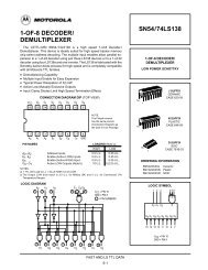
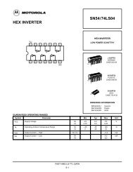
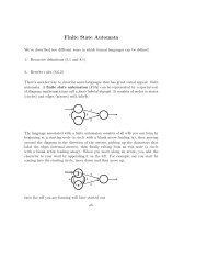
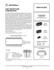
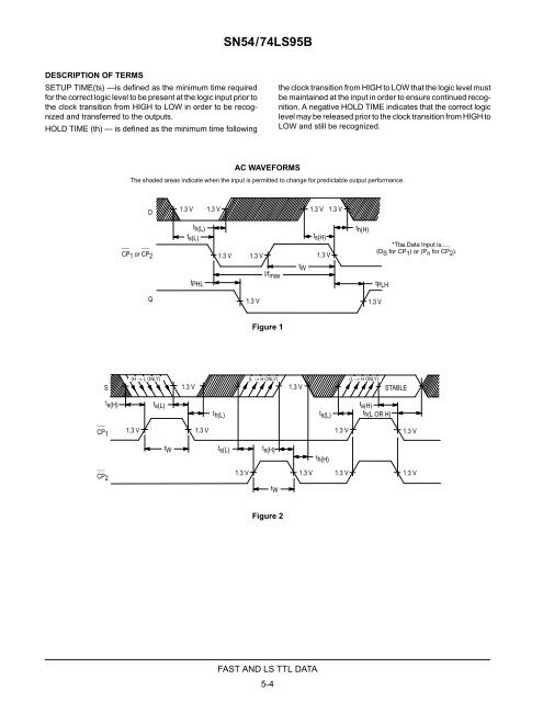
<strong>SN54</strong>/<strong>74LS95B</strong>DESCRIPTION OF TERMSSETUP TIME(ts) —is defined as the minimum time requiredfor the correct logic level to be present at the logic input prior tothe clock transition from HIGH to LOW in order to be recognizedand transferred to the outputs.HOLD TIME (th) — is defined as the minimum time followingthe clock transition from HIGH to LOW that the logic level mustbe maintained at the input in order to ensure continued recognition.A negative HOLD TIME indicates that the correct logiclevel may be released prior to the clock transition from HIGH toLOW and still be recognized.AC WAVEFORMSThe shaded areas indicate when the input is permitted to change for predictable output performance.D1.3 V 1.3 V 1.3 V 1.3 VCP1 or CP2th(L)ts(L)1.3 V 1.3 Vts(H)1.3 Vth(H)*The Data Input is(D S for CP 1 ) or (P n for CP 2 ).tPHLl/fmaxtWtPLHQ1.3 V1.3 VFigure 1S(H → L ONLY)(L → H ONLY) (L → H ONLY)1.3 V 1.3 VSTABLEts(H)ts(L)th(L)ts(L)ts(H)th(L OR H)CP11.3 V 1.3 V1.3 V1.3 VtWts(L)ts(H)th(H)CP21.3 V1.3 V1.3 V1.3 VtWFigure 2FAST AND LS TTL DATA5-4