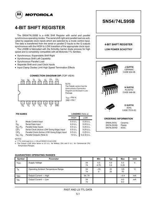
4-BIT SHIFT REGISTER SN54/74LS95B
4-BIT SHIFT REGISTER SN54/74LS95B
4-BIT SHIFT REGISTER SN54/74LS95B

Create successful ePaper yourself
Turn your PDF publications into a flip-book with our unique Google optimized e-Paper software.
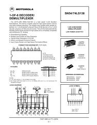
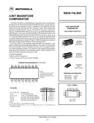
4-<strong>BIT</strong> <strong>SHIFT</strong> <strong>REGISTER</strong><strong>SN54</strong>/<strong>74LS95B</strong>The <strong>SN54</strong>/<strong>74LS95B</strong> is a 4-Bit Shift Register with serial and parallelsynchronous operating modes. The serial shift right and parallel load are activatedby separate clock inputs which are selected by a mode control input.The data is transferred from the serial or parallel D inputs to the Q outputssynchronous with the HIGH to LOW transition of the appropriate clock input.The LS95B is fabricated with the Schottky barrier diode process for highspeed and is completely compatible with all Motorola TTL families.• Synchronous, Expandable Shift Right• Synchronous Shift Left Capability• Synchronous Parallel Load• Separate Shift and Load Clock Inputs• Input Clamp Diodes Limit High Speed Termination EffectsCONNECTION DIAGRAM DIP (TOP VIEW)VCC Q0 Q1 Q2 Q3 CP1 CP214 13 12 11 10 9 81 2 3 4 5 6 7DS P0 P1 P2 P3 S GNDNOTE:The Flatpak version has thesame pinouts (ConnectionDiagram) as the Dual In-LinePackage.VCC = PIN 14GND = PIN 7PIN NAMES LOADING (Note a)HIGH LOWS Mode Control Input 0.5 U.L. 0.25 U.L.DS Serial Data Input 0.5 U.L. 0.25 U.L.P0–P3 Parallel Data Inputs 0.5 U.L. 0.25 U.L.CP1 Serial Clock (Active LOW Going Edge) Input 0.5 U.L. 0.25 U.L.CP2 Parallel Clock (Active LOW Going Edge) Input 0.5 U.L. 0.25 U.L.Q0–Q3 Parallel Outputs (Note b) 10 U.L. 5 (2.5) U.L.NOTES:a. 1 TTL Unit Load (U.L.) = 40 µA HIGH/1.6 mA LOW.b. The Output LOW drive factor is 2.5 U.L. for Military (54) and 5 U.L. for Commercial (74)Temperature Ranges.14144-<strong>BIT</strong> <strong>SHIFT</strong> <strong>REGISTER</strong>LOW POWER SCHOTTKY11141J SUFFIXCERAMICCASE 632-08N SUFFIXPLASTICCASE 646-06ORDERING INFORMATION<strong>SN54</strong>LSXXJSN74LSXXNSN74LSXXDD SUFFIXSOICCASE 751A-02CeramicPlasticSOICGUARANTEED OPERATING RANGESSymbol Parameter Min Typ Max UnitVCC Supply Voltage 54744.54.755.05.05.55.25VTA Operating Ambient Temperature Range 5474–550252512570°CIOH Output Current — High 54, 74 –0.4 mAIOL Output Current — Low 54744.08.0mAFAST AND LS TTL DATA5-1
<strong>SN54</strong>/<strong>74LS95B</strong>SDS61LOGIC DIAGRAMP0 P1P2 P32 34 5CP19CP28RRRRVCC = PIN 14GND = PIN 7= PIN NUMBERSSQSQS1312 1110Q0 Q1 Q2 Q3QSQFUNCTIONAL DESCRIPTIONThe LS95B is a 4-Bit Shift Register with serial and parallelsynchronous operating modes. It has a Serial (DS) and fourParallel (P0–P3) Data inputs and four Parallel Data outputs(Q0–Q3). The serial or parallel mode of operation is controlledby a Mode Control input (S) and two Clock Inputs (CP1) and(CP2). The serial (right-shift) or parallel data transfers occursynchronous with the HIGH to LOW transition of the selectedclock input.When the Mode Control input (S) is HIGH, CP2 is enabled. AHIGH to LOW transition on enabled CP2 transfers paralleldata from the P0–P3 inputs to the Q0–Q3 outputs.When the Mode Control input (S) is LOW, CP1 is enabled. AHIGH to LOW transition on enabled CP1 transfers the datafrom Serial input (DS) to Q0 and shifts the data in Q0 to Q1, Q1to Q2, and Q2 to Q3 respectively (right-shift). A left-shift is accomplishedby externally connecting Q3 to P2, Q2 to P1, andQ1 to P0, and operating the LS95B in the parallel mode (S =HIGH).For normal operation, S should only change states whenboth Clock inputs are LOW. However, changing S from LOWto HIGH while CP2 is HIGH, or changing S from HIGH to LOWwhile CP1 is HIGH and CP2 is LOW will not cause any changeson the register outputs.MODE SELECT — TRUTH TABLEINPUTSOUTPUTSOPERATING MODES CP1 CP2 DS Pn Q0 Q1 Q2 Q3ShiftL X I X L q0 q1 q2L X h X H q0 q1 q2Parallel Load H X X Pn P0 P1 P2 P3L L X X No ChangeL L X X No ChangeH L X X No ChangeMode Change H L X X UndeterminedL H X X UndeterminedL H X X No ChangeH H X X UndeterminedH H X X No ChangeL = LOW Voltage LevelH = HIGH Voltage LevelX = Don’t CareI = LOW Voltage Level one set-up time prior to the HIGH to LOW clock transition.h = HIGH Voltage Level one set-up time prior to the HIGH to LOW clock transition.P n = Lower case letters indicate the state of the referenced input (or output) one set-up time prior to the Pn= HIGH to LOW clock transition.FAST AND LS TTL DATA5-2
<strong>SN54</strong>/<strong>74LS95B</strong>DC CHARACTERISTICS OVER OPERATING TEMPERATURE RANGE (unless otherwise specified)LimitsSymbol Parameter Min Typ Max Unit Test ConditionsiVIH Input HIGH Voltage 2.0 VVILInput LOW Voltage54 0.774 0.8VGuaranteed Input HIGH Voltage forAll InputsGuaranteed Input LOW Voltage forAll InputsVIK Input Clamp Diode Voltage –0.65 –1.5 V VCC = MIN, IIN = – 18 mAVOHVOLOutput HIGH VoltageOutput LOW Voltage54 2.5 3.5 V VCC = MIN, IOH = MAX, VIN = VIH74 2.7 3.5 Vor VIL per Truth Table54, 74 0.25 0.4 V IOL = 4.0 mA VCC = VCC MIN,VIN =VIL or VIH74 0.35 0.5 V IOL = 8.0 mA per Truth TableIIHInput HIGH Current20 µA VCC = MAX, VIN = 2.7 V0.1 mA VCC = MAX, VIN = 7.0 VIIL Input HIGH Current –0.4 mA VCC = MAX, VIN = 0.4 VIOS Short Circuit Current (Note 1) –20 –100 mA VCC = MAXICC Power Supply Current 21 mA VCC = MAXNote 1: Not more than one output should be shorted at a time, nor for more than 1 second.AC CHARACTERISTICS (TA = 25°C, VCC = 5.0 V)LimitsSymbol Parameter Min Typ Max Unit Test ConditionsifMAX Maximum Clock Frequency 25 36 MHz18 27 nsVCC = 5.0 VtPLHCP to OutputCL = 15 pFtPHL21 32 nsAC SETUP REQUIREMENTS (TA = 25°C, VCC = 5.0 V)LimitsSymbol Parameter Min Typ Max Unit Test ConditionsitW CP Pulse Width 20 nsts Data Setup Time 20 nsth Data Hold Time 20 ns VCC = 5.0 Vts Mode Control Setup Time 20 nsth Mode Control Hold Time 20 nsFAST AND LS TTL DATA5-3
<strong>SN54</strong>/<strong>74LS95B</strong>DESCRIPTION OF TERMSSETUP TIME(ts) —is defined as the minimum time requiredfor the correct logic level to be present at the logic input prior tothe clock transition from HIGH to LOW in order to be recognizedand transferred to the outputs.HOLD TIME (th) — is defined as the minimum time followingthe clock transition from HIGH to LOW that the logic level mustbe maintained at the input in order to ensure continued recognition.A negative HOLD TIME indicates that the correct logiclevel may be released prior to the clock transition from HIGH toLOW and still be recognized.AC WAVEFORMSThe shaded areas indicate when the input is permitted to change for predictable output performance.D1.3 V 1.3 V 1.3 V 1.3 VCP1 or CP2th(L)ts(L)1.3 V 1.3 Vts(H)1.3 Vth(H)*The Data Input is(D S for CP 1 ) or (P n for CP 2 ).tPHLl/fmaxtWtPLHQ1.3 V1.3 VFigure 1S(H → L ONLY)(L → H ONLY) (L → H ONLY)1.3 V 1.3 VSTABLEts(H)ts(L)th(L)ts(L)ts(H)th(L OR H)CP11.3 V 1.3 V1.3 V1.3 VtWts(L)ts(H)th(H)CP21.3 V1.3 V1.3 V1.3 VtWFigure 2FAST AND LS TTL DATA5-4