Si6875DQ Dual P-Channel 20-V (D-S) MOSFET, Common Drain
Si6875DQ Dual P-Channel 20-V (D-S) MOSFET, Common Drain
Si6875DQ Dual P-Channel 20-V (D-S) MOSFET, Common Drain

Create successful ePaper yourself
Turn your PDF publications into a flip-book with our unique Google optimized e-Paper software.
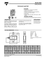
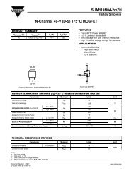
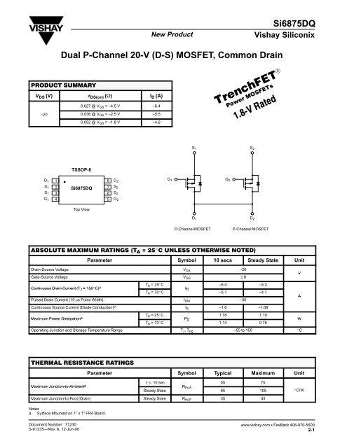
New Product<strong>Si6875DQ</strong>Vishay Siliconix<strong>Dual</strong> P-<strong>Channel</strong> <strong>20</strong>-V (D-S) <strong>MOSFET</strong>, <strong>Common</strong> <strong>Drain</strong> V DS (V) r DS(on) () I D (A)0.027 @ V GS = –4.5 V –6.4–<strong>20</strong> 0.036 @ V GS = –2.5 V –5.50.052 @ V GS = –1.8 V –4.6S 1S 2TSSOP-8D 1 1S 1 2S 1 3G 1 4<strong>Si6875DQ</strong>8765D 2S 2S 2G 2G 1D 1G 2D 2Top ViewP-<strong>Channel</strong> <strong>MOSFET</strong>P-<strong>Channel</strong> <strong>MOSFET</strong> Parameter Symbol 10 secs Steady State Unit<strong>Drain</strong>-Source Voltage V DS –<strong>20</strong>VGate-Source Voltage V GS 8Continuous <strong>Drain</strong> Current (T J = 150C) aT A = 25CI D–6.4 –5.2T A = 70C–5.1 –4.1APulsed <strong>Drain</strong> Current (10 s Pulse Width) I DM –30Continuous Source Current (Diode Conduction) a I S –1.6 –1.08Maximum Power Dissipation aT A = 25CP D1.78 1.19WT A = 70C1.14 0.76Operating Junction and Storage Temperature Range T J , T stg –55 to 150 C Parameter Symbol Typical Maximum UnitMaximum Junction-to-Ambient at 10 secSteady State55 70R thJA85 105 C/WMaximum Junction-to-Foot (<strong>Drain</strong>) Steady State R thJF 35 45Notesa. Surface Mounted on 1” x 1” FR4 Board.Document Number: 71230S-01235—Rev. A, 12-Jun-00www.vishay.com FaxBack 408-970-56002-1
<strong>Si6875DQ</strong>Vishay SiliconixNew Product Parameter Symbol Test Condition Min Typ Max UnitStaticGate Threshold Voltage V GS(th) V DS = V GS , I D = –250 A –0.45 VGate-Body Leakage I GSSV DS = 0 V, V GS = 8 V 100 nAZero Gate Voltage <strong>Drain</strong> Current IV DS = –16 V, V GS = 0 V –1DSSV DS = –16 V, V GS = 0 V, T J = 70C –25AOn-State <strong>Drain</strong> Current a I D(on) V DS = –5 V, V GS = –4.5 V –<strong>20</strong> AV GS = –4.5 V, I D = –6.4 A 0.022 0.027<strong>Drain</strong>-Source On-State Resistance a r DS(on) V GS = –2.5 V, I D = –5.5 A 0.029 0.036V GS = –1.8 V, I D = –4.6 A 0.042 0.052 Forward Transconductance a g fs V DS = –5 V, I D = –6.4 A 19 SDiode Forward Voltage a V SD I S = –1.6 A, V GS = 0 V –0.70 –1.1 VDynamic bTotal Gate Charge Q g 26 36Gate-Source Charge Q gs V DS = –10 V, V GS = –4.5 V, I D = –6.4 A 4.6 nCGate-<strong>Drain</strong> Charge Q gd 5.9Turn-On Delay Time t d(on)Rise Time t r V VDD = –10 V, R L = 10 Turn-Off Delay Time t I d(off) D –1 A, V GEN = –4.5 V, R G = 6 26 4027 40170 250 nsFall Time t f 75 110Source-<strong>Drain</strong> Reverse Recovery Time t rr I F = –1.6 A, di/dt = 100 A/s 30 50Notesa. Pulse test; pulse width 300 s, duty cycle 2%.b. Guaranteed by design, not subject to production testing. 30Output Characteristics30Transfer Characteristics24V GS = 5 thru 2.5 V2 V24T C = –55C25C– <strong>Drain</strong> Current (A)I D181261.5 V– <strong>Drain</strong> Current (A)I D18126125C0.5, 1 V00 3 6 9 12V DS – <strong>Drain</strong>-to-Source Voltage (V)00 0.5 1.0 1.5 2.0 2.5V GS – Gate-to-Source Voltage (V)www.vishay.com FaxBack 408-970-56002-2Document Number: 71230S-01235—Rev. A, 12-Jun-00
New Product<strong>Si6875DQ</strong>Vishay Siliconix 0.10On-Resistance vs. <strong>Drain</strong> Current4000Capacitancer DS(on) – On-Resistance ( )0.080.060.040.02V GS = 1.8 VV GS = 2.5 VV GS = 4.5 VC – Capacitance (pF)350030002500<strong>20</strong>0015001000500C ossC iss00 6 12 18 24 30I D – <strong>Drain</strong> Current (A)C rss00 4 8 12 16 <strong>20</strong>V DS – <strong>Drain</strong>-to-Source Voltage (V)5Gate Charge1.6On-Resistance vs. Junction Temperature– Gate-to-Source Voltage (V)V GS4321V DS = 10 VI D = 6.4 Ar DS(on) – On-Resistance ( )(Normalized)1.41.21.00.8V GS = 4.5 VI D = 6.4 A00 6 12 18 24 30Q g – Total Gate Charge (nC)0.6–50 –25 0 25 50 75 100 125 150T J – Junction Temperature (C)30Source-<strong>Drain</strong> Diode Forward Voltage0.08On-Resistance vs. Gate-to-Source Voltage– Source Current (A)I S10T J = 150CT J = 25Cr DS(on) – On-Resistance ( )0.060.040.02I D = 6.4 A10 0.2 0.4 0.6 0.8 1.0 1.2 1.4V SD – Source-to-<strong>Drain</strong> Voltage (V)00 2 4 6 8V GS – Gate-to-Source Voltage (V)Document Number: 71230S-01235—Rev. A, 12-Jun-00www.vishay.com FaxBack 408-970-56002-3
<strong>Si6875DQ</strong>Vishay SiliconixNew Product 0.5Threshold Voltage100Single Pulse Power, Junction-to-Ambient0.480Variance (V)V GS(th)0.30.<strong>20</strong>.10.0I D = 250 APower (W)6040–0.1<strong>20</strong>–0.2–50 –25 0 25 50 75 100 125 15000.0010.010.1 110T J – Temperature (C)Time (sec)2Normalized Thermal Transient Impedance, Junction-to-AmbientNormalized Effective TransientThermal Impedance1Duty Cycle = 0.50.2Notes:0.10.1P DM0.05t 1t 2 t 10.021. Duty Cycle, D =t 22. Per Unit Base = R thJA = 85C/W3. T JM – T A = P DM Z (t) thJASingle Pulse4. Surface Mounted0.0110 –4 10 –3 10 –2 10 –11 10 100600Square Wave Pulse Duration (sec)2Normalized Thermal Transient Impedance, Junction-to-FootNormalized Effective TransientThermal Impedance10.1Duty Cycle = 0.50.<strong>20</strong>.10.050.02Single Pulse0.0110 –410 –3 10 –2 10 –11 10Square Wave Pulse Duration (sec)www.vishay.com FaxBack 408-970-56002-4Document Number: 71230S-01235—Rev. A, 12-Jun-00