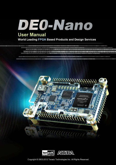
User Manual - Terasic
User Manual - Terasic
User Manual - Terasic
- No tags were found...

Create successful ePaper yourself
Turn your PDF publications into a flip-book with our unique Google optimized e-Paper software.
Chapter 1IntroductionThe DE0-Nano board introduces a compact-sized FPGA development platform suited for to a widerange of portable design projects, such as robots and mobile projects.The DE0-Nano is ideal for use with embedded soft processors—it features a powerful Altera CycloneIV FPGA (with 22,320 logic elements), 32 MB of SDRAM, 2 Kb EEPROM, and a 64 Mb serialconfiguration memory device. For connecting to real-world sensors the DE0-Nano includes aNational Semiconductor 8-channel 12-bit A/D converter, and it also features an Analog Devices13-bit, 3-axis accelerometer device.The DE0-Nano board includes a built-in USB Blaster for FPGA programming, and the board can bepowered either from this USB port or by an external power source. The board includes expansionheaders that can be used to attach various <strong>Terasic</strong> daughter cards or other devices, such as motorsand actuators. Inputs and outputs include 2 pushbuttons, 8 user LEDs and a set of 4 dip-switches.1.1 FeaturesFigure 1-1 shows a photograph of the DE0-Nano Board.Figure 1-1 The DE0-Nano Board4
The key features of the board are listed below:• Featured deviceo Altera Cyclone® IV EP4CE22F17C6N FPGAo 153 maximum FPGA I/O pins• Configuration status and set-up elementso On-board USB-Blaster circuit for programmingo Spansion EPCS64• Expansion headero Two 40-pin Headers (GPIOs) provide 72 I/O pins, 5V power pins, two 3.3V power pins andfour ground pins• Memory deviceso 32MB SDRAMo 2Kb I2C EEPROM• General user input/outputo 8 green LEDso 2 debounced pushbuttonso 4-position DIP switch• G-Sensoro ADI ADXL345, 3-axis accelerometer with high resolution (13-bit)• A/D Convertero NS ADC128S022, 8-Channel, 12-bit A/D Convertero 50 Ksps to 200 Ksps• Clock systemo On-board 50MHz clock oscillator• Power Supplyo USB Type mini-AB port (5V)o DC 5V pin for each GPIO header (2 DC 5V pins)o 2-pin external power header (3.6-5.7V)5
1.2 About the KITThe kit comes with the following contents:• DE0-Nano board• System CD-ROM.• USB CableThe system CD contains technical documents for the DE0-Nano board, which includes componentdatasheets, demonstrations, schematic, and user manual.Figure 1-2 shows the photograph of the DE0-Nano kit contents.Figure 1-2 DE0-Nano kit package contents1.3 Getting HelpHere is information of how to get help if you encounter any problem:• <strong>Terasic</strong> Technologies• Tel: +886-3-575-0880• Email: support@terasic.com• Altera Corporation• Email: university@altera.com6
Figure 2-2 The DE0-Nano Board PCB and component diagram (bottom view)2.2 Block Diagram of the DE0-Nano BoardFigure 2-3 shows the block diagram of the DE0-Nano board. To provide maximum flexibility forthe user, all connections are made through the Cyclone IV FPGA device. Thus, the user canconfigure the FPGA to implement any system design.Figure 2-3 Block diagram of DE0-Nano Board8
2.3 Power-up the DE0-Nano BoardThe DE0-Nano board comes with a preloaded configuration bit stream to demonstrate somefeatures of the board. This allows users to see quickly if the board is working properly. To power-upthe board two options are available which are described below:1. Connect a USB Mini-B cable between a USB (Type A) host port and the board. Forcommunication between the host and the DE0-Nano board, it is necessary to install the Altera USBBlaster driver software.2. Alternatively, users can power-up the DE0-Nano board by supplying 5V to the two DC +5(VCC5) pins of the GPIO headers or supplying (3.6-5.7V) to the 2-pin header.At this point you should observe flashing LEDs on the board.9
Chapter 3Using the DE0-Nano BoardThis chapter gives instructions for using the DE0-Nano board and describes in detail its componentsand connectors, along with the required pin assignments.3.1 Configuring the Cyclone IV FPGAThe DE0-Nano board contains a Cyclone IV E FPGA which can be programmed using JTAGprogramming. This allows users to configure the FPGA with a specified design using Quartus IIsoftware. The programmed design will remain functional on the FPGA as long as the board ispowered on, or until the device is reprogrammed. The configuration information will be lost whenthe power is turned off.To download a configuration bit stream file using JTAG Programming into the Cyclone IV FPGA,perform the following steps:1. Connect a USB Mini-B cable between a host computer and the DE0-Nano.2. The FPGA can now be programmed through the Quartus II Programmer by selecting aconfiguration bit stream file with the .sof filename extension.• Configuring the Spansion EPCS64 deviceThe DE0-Nano board contains a Spansion EPCS64 serial configuration device. This deviceprovides non-volatile storage of the configuration bit-stream, so that the information is retainedeven when the power supply to the DE0-Nano board is turned off. When the board’s power isturned on, the configuration data in the EPCS64 device is automatically loaded into the Cyclone IVE FPGA.The Cyclone IV E device supports in-system programming of a serial configuration device usingthe JTAG interface via the serial flash loader design. The serial flash loader is a bridge design forthe Cyclone IV E device that uses its JTAG interface to access the EPCS .jic file and then uses theAS interface to program the EPCS device. Figure 3-1 illustrates the programming method whenadopting a serial flash loader solution. Chapter 9 of this document describes how to load a circuit tothe serial configuration device.10
Figure 3-1 Programming a serial configuration device with serial flash loader solution• JTAG Chain on DE0-Nano BoardThe JTAG Chain on the DE0-Nano board is connected to a host computer using an on-boardUSB-blaster. The USB-blaster consists of a USB Mini-B connector, a FTDI USB 2.0 Controller,and an Altera MAX II CPLD.Figure 3-2 illustrates the JTAG configuration setup.Figure 3-2 JTAG Chain3.2 General <strong>User</strong> Input/Output• PushbuttonsThe DE0-Nano board contains two pushbuttons shown in Figure 3-3. Each pushbutton isdebounced using a Schmitt Trigger circuit, as indicated in Figure 3-4. The two outputs called KEY0,and KEY1 of the Schmitt Trigger devices are connected directly to the Cyclone IV E FPGA. Eachpushbutton provides a high logic level when it is not pressed, and provides a low logic level whenpressed. Since the pushbuttons are debounced, they are appropriate for using as clock or resetinputs.11
DRAM_ADDR[12] PIN_L4 SDRAM Address[12] 3.3VDRAM_DQ[0] PIN_G2 SDRAM Data[0] 3.3VDRAM_DQ[1] PIN_G1 SDRAM Data[1] 3.3VDRAM_DQ[2] PIN_L8 SDRAM Data[2] 3.3VDRAM_DQ[3] PIN_K5 SDRAM Data[3] 3.3VDRAM_DQ[4] PIN_K2 SDRAM Data[4] 3.3VDRAM_DQ[5] PIN_J2 SDRAM Data[5] 3.3VDRAM_DQ[6] PIN_J1 SDRAM Data[6] 3.3VDRAM_DQ[7] PIN_R7 SDRAM Data[7] 3.3VDRAM_DQ[8] PIN_T4 SDRAM Data[8] 3.3VDRAM_DQ[9] PIN_T2 SDRAM Data[9] 3.3VDRAM_DQ[10] PIN_T3 SDRAM Data[10] 3.3VDRAM_DQ[11] PIN_R3 SDRAM Data[11] 3.3VDRAM_DQ[12] PIN_R5 SDRAM Data[12] 3.3VDRAM_DQ[13] PIN_P3 SDRAM Data[13] 3.3VDRAM_DQ[14] PIN_N3 SDRAM Data[14] 3.3VDRAM_DQ[15] PIN_K1 SDRAM Data[15] 3.3VDRAM_BA[0] PIN_M7 SDRAM Bank Address[0] 3.3VDRAM_BA[1] PIN_M6 SDRAM Bank Address[1] 3.3VDRAM_DQM[0] PIN_R6 SDRAM byte Data Mask[0] 3.3VDRAM_DQM[1] PIN_T5 SDRAM byte Data Mask[1] 3.3VDRAM_RAS_N PIN_L2 SDRAM Row Address Strobe 3.3VDRAM_CAS_N PIN_L1 SDRAM Column Address Strobe 3.3VDRAM_CKE PIN_L7 SDRAM Clock Enable 3.3VDRAM_CLK PIN_R4 SDRAM Clock 3.3VDRAM_WE_N PIN_C2 SDRAM Write Enable 3.3VDRAM_CS_N PIN_P6 SDRAM Chip Select 3.3V3.4 I2C Serial EEPROMThe DE0-Nano contains a 2Kbit Electrically Erasable PROM (EEPROM). The EEPROM isconfigured through a 2-wire I2C serial interface. The device is organized as one block of 256 x 8-bitmemory. The I2C write and read address are 0xA0 and 0xA1, respectively. Figure 3-7 illustrates itsconnections with the Cyclone IV FPGA.15
Figure 3-7 Connections between FPGA and EEPROMTable 3-5 Pin Assignments for I2C Serial EEPROMSignal Name FPGA Pin No. Description I/O StandardI2C_SCLK PIN_F2 EEPROM clock 3.3VI2C_SDAT PIN_F1 EEPROM data 3.3V3.5 Expansion HeadersThe DE0-Nano board provides two 40-pin expansion headers. Each header connects directly to 36pins of the Cyclone IV E FPGA, and also provides DC +5V (VCC5), DC +3.3V (VCC33), and twoGND pins. Figure 3-8 shows the I/O distribution of the GPIO connectors.16
Figure 3-8 Pin arrangement of the GPIO expansion headersThe pictures below indicate the pin 1 location of the expansion headers.Figure 3-9 Pin1 locations of the GPIO expansion headersTable 3-6 GPIO-0 Pin AssignmentsSignal Name FPGA Pin No. Description I/O StandardGPIO_0_IN0 PIN_A8 GPIO Connection DATA 3.3VGPIO_00 PIN_D3 GPIO Connection DATA 3.3VGPIO_0_IN1 PIN_B8 GPIO Connection DATA 3.3VGPIO_01 PIN_C3 GPIO Connection DATA 3.3VGPIO_02 PIN_A2 GPIO Connection DATA 3.3V17
GPIO_03 PIN_A3 GPIO Connection DATA 3.3VGPIO_04 PIN_B3 GPIO Connection DATA 3.3VGPIO_05 PIN_B4 GPIO Connection DATA 3.3VGPIO_06 PIN_A4 GPIO Connection DATA 3.3VGPIO_07 PIN_B5 GPIO Connection DATA 3.3VGPIO_08 PIN_A5 GPIO Connection DATA 3.3VGPIO_09 PIN_D5 GPIO Connection DATA 3.3VGPIO_010 PIN_B6 GPIO Connection DATA 3.3VGPIO_011 PIN_A6 GPIO Connection DATA 3.3VGPIO_012 PIN_B7 GPIO Connection DATA 3.3VGPIO_013 PIN_D6 GPIO Connection DATA 3.3VGPIO_014 PIN_A7 GPIO Connection DATA 3.3VGPIO_015 PIN_C6 GPIO Connection DATA 3.3VGPIO_016 PIN_C8 GPIO Connection DATA 3.3VGPIO_017 PIN_E6 GPIO Connection DATA 3.3VGPIO_018 PIN_E7 GPIO Connection DATA 3.3VGPIO_019 PIN_D8 GPIO Connection DATA 3.3VGPIO_020 PIN_E8 GPIO Connection DATA 3.3VGPIO_021 PIN_F8 GPIO Connection DATA 3.3VGPIO_022 PIN_F9 GPIO Connection DATA 3.3VGPIO_023 PIN_E9 GPIO Connection DATA 3.3VGPIO_024 PIN_C9 GPIO Connection DATA 3.3VGPIO_025 PIN_D9 GPIO Connection DATA 3.3VGPIO_026 PIN_E11 GPIO Connection DATA 3.3VGPIO_027 PIN_E10 GPIO Connection DATA 3.3VGPIO_028 PIN_C11 GPIO Connection DATA 3.3VGPIO_029 PIN_B11 GPIO Connection DATA 3.3VGPIO_030 PIN_A12 GPIO Connection DATA 3.3VGPIO_031 PIN_D11 GPIO Connection DATA 3.3VGPIO_032 PIN_D12 GPIO Connection DATA 3.3VGPIO_033 PIN_B12 GPIO Connection DATA 3.3VTable 3-7 GPIO-1 Pin AssignmentsSignal Name FPGA Pin No. Description I/O StandardGPIO_1_IN0 PIN_T9 GPIO Connection DATA 3.3VGPIO_10 PIN_F13 GPIO Connection DATA 3.3VGPIO_1_IN1 PIN_R9 GPIO Connection DATA 3.3VGPIO_11 PIN_T15 GPIO Connection DATA 3.3VGPIO_12 PIN_T14 GPIO Connection DATA 3.3VGPIO_13 PIN_T13 GPIO Connection DATA 3.3VGPIO_14 PIN_R13 GPIO Connection DATA 3.3VGPIO_15 PIN_T12 GPIO Connection DATA 3.3VGPIO_16 PIN_R12 GPIO Connection DATA 3.3V18
GPIO_17 PIN_T11 GPIO Connection DATA 3.3VGPIO_18 PIN_T10 GPIO Connection DATA 3.3VGPIO_19 PIN_R11 GPIO Connection DATA 3.3VGPIO_110 PIN_P11 GPIO Connection DATA 3.3VGPIO_111 PIN_R10 GPIO Connection DATA 3.3VGPIO_112 PIN_N12 GPIO Connection DATA 3.3VGPIO_113 PIN_P9 GPIO Connection DATA 3.3VGPIO_114 PIN_N9 GPIO Connection DATA 3.3VGPIO_115 PIN_N11 GPIO Connection DATA 3.3VGPIO_116 PIN_L16 GPIO Connection DATA 3.3VGPIO_117 PIN_K16 GPIO Connection DATA 3.3VGPIO_118 PIN_R16 GPIO Connection DATA 3.3VGPIO_119 PIN_L15 GPIO Connection DATA 3.3VGPIO_120 PIN_P15 GPIO Connection DATA 3.3VGPIO_121 PIN_P16 GPIO Connection DATA 3.3VGPIO_122 PIN_R14 GPIO Connection DATA 3.3VGPIO_123 PIN_N16 GPIO Connection DATA 3.3VGPIO_124 PIN_N15 GPIO Connection DATA 3.3VGPIO_125 PIN_P14 GPIO Connection DATA 3.3VGPIO_126 PIN_L14 GPIO Connection DATA 3.3VGPIO_127 PIN_N14 GPIO Connection DATA 3.3VGPIO_128 PIN_M10 GPIO Connection DATA 3.3VGPIO_129 PIN_L13 GPIO Connection DATA 3.3VGPIO_130 PIN_J16 GPIO Connection DATA 3.3VGPIO_131 PIN_K15 GPIO Connection DATA 3.3VGPIO_132 PIN_J13 GPIO Connection DATA 3.3VGPIO_133 PIN_J14 GPIO Connection DATA 3.3V3.6 A/D Converter and 2x13 HeaderThe DE0-Nano contains an ADC128S022 lower power, eight-channel CMOS 12-bitanalog-to-digital converter. This A-to-D provides conversion throughput rates of 50 ksps to 200ksps. It can be configured to accept up to eight input signals at inputs IN0 through IN7. This eightinput signals are connected to the 2x13 header, as shown in Figure 3-10. The remaining I/Os of the2x13 header are a DC +3.3V (VCC33), a GND and 13 pins, which are connect directly to theCyclone IV E device.For more detailed information on the A/D converter chip, please refer to its datasheet which isavailable on manufacturer’s website or under the /datasheet folder of the system CD.19
Figure 3-10 Pin distribution of the 2x13 HeaderFigure 3-11 shows the connections on the 2x13 header, A/D converter and Cyclone IV device.Figure 3-11 Wiring for 2x13 header and A/D converterThe pictures below indicate the pin 1 location of the 2x13 header.20
Figure 3-12 Pin1 locations of the 2x13 headerTable 3-8 Pin Assignments for 2x13 HeaderSignal Name FPGA Pin No. Description I/O StandardGPIO_2[0] PIN_A14 GPIO Connection DATA[0] 3.3VGPIO_2[1] PIN_B16 GPIO Connection DATA[1] 3.3VGPIO_2[2] PIN_C14 GPIO Connection DATA[2] 3.3VGPIO_2[3] PIN_C16 GPIO Connection DATA[3] 3.3VGPIO_2[4] PIN_C15 GPIO Connection DATA[4] 3.3VGPIO_2[5] PIN_D16 GPIO Connection DATA[5] 3.3VGPIO_2[6] PIN_D15 GPIO Connection DATA[6] 3.3VGPIO_2[7] PIN_D14 GPIO Connection DATA[7] 3.3VGPIO_2[8] PIN_F15 GPIO Connection DATA[8] 3.3VGPIO_2[9] PIN_F16 GPIO Connection DATA[9] 3.3VGPIO_2[10] PIN_F14 GPIO Connection DATA[10] 3.3VGPIO_2[11] PIN_G16 GPIO Connection DATA[11] 3.3VGPIO_2[12] PIN_G15 GPIO Connection DATA[12] 3.3VGPIO_2_IN[0] PIN_E15 GPIO Input 3.3VGPIO_2_IN[1] PIN_E16 GPIO Input 3.3VGPIO_2_IN[2] PIN_M16 GPIO Input 3.3VTable 3-9 Pin Assignments for ADCSignal Name FPGA Pin No. Description I/O StandardADC_CS_N PIN_A10 Chip select 3.3VADC_SADDR PIN_B10 Digital data input 3.3VADC_SDAT PIN_A9 Digital data output 3.3VADC_SCLK PIN_B14 Digital clock input 3.3V21
3.7 Digital AccelerometerThe ADXL345 is a small, thin, ultralow power, 3-axis accelerometer with high resolutionmeasurement. This digital accelerometer can be accessed through a SPI 3-wire digital interface orI2C 2-wire digital interface. Main applications include medical instrumentation, industrialinstrumentation, personal electronic aid and hard disk drive protection etc. Some of the key featuresof this device are listed below. For more detailed information, please refer to its datasheet which isavailable on manufacturer’s website or under the /datasheet folder of the system CD.• Up to 13-bit resolution at +/- 16g• SPI (3- wire) or I2C (2-wire) digital interface• Flexible interrupts modesFigure 3-13 shows the connections between the ADXL345 and the Cyclone IV E device.Figure 3-13 Wiring between the ADXL345 and the Cyclone IV E deviceTable 3-10 Pin Assignments for Digital AccelerometerSignal Name FPGA Pin No. Description I/O StandardI2C_SCLK PIN_F2 EEPROM clock 3.3VI2C_SDAT PIN_F1 EEPROM data 3.3VG_SENSOR_INT PIN_M2 G_Sensor Interrupt 3.3VG_SENSOR_CS_N PIN_G5 G_Sensor chip select 3.3V3.8 Clock CircuitryThe DE0-Nano board includes a 50 MHz oscillator. The oscillator is connected directly to adedicated clock input pin of the Cyclone IV E FPGA. The 50MHz clock input can be used as asource clock to drive the phase lock loops (PLL) circuit. The clock distribution on the DE0-Nanoboard is shown in Figure 3-14.22
Figure 3-14 Block diagram of the clock distribution3.9 Power SupplyThe DE0-Nano board’s power is provided through the USB 5V power, the 5V VCC pins on the two40-pin headers or the 2-pin power header. The DC voltage is then stepped down to various requiredvoltages. For portable project applications, connect a battery power supply (3.6~5.7V) to the 2-pinexternal power header shown in Figure 3-15.Figure 3-15 Portable Battery Connection23
• Power Distribution SystemFigure 3-16 shows the power distribution system on the DE0-Nano board.Figure 3-16 DE0-Nano Power Distribution System24
Chapter 4DE0-Nano Control PanelThe DE0-Nano board comes with a Control Panel facility that allows users to access variouscomponents on the board from a host computer. The host computer communicates with the boardthrough a USB connection. The facility can be used to verify the functionality of components on theboard or be used as a debug tool while developing RTL code.This chapter first presents some basic functions of the Control Panel, then describes its structure inblock diagram form, and finally describes its capabilities.4.1 Control Panel SetupThe Control Panel Software Utility is located in the directory “tools/DE0_NANO_ControlPanel” inthe DE0-Nano System CD. It's free of installation, just copy the whole folder to your host computerand launch the control panel by executing the “DE0_NANO_ControlPanel.exe”.When Control Panel starts it will attempt to download a configuration file onto the DE0-Nano board.The configuration file contains a design that communicates with the peripheral devices on the boardthat are attached to the FPGA device. Perform the following steps to ensure that the control panelstarts up successfully:1. Make sure Quartus II 10.0 or later version is installed successfully on your PC.2. Connect a USB A to Mini-B cable to a USB (Type A) host port and to the board.3. Start the executable DE0_NANO_ControlPanel.exe on the host computer. The Control Paneluser interface shown in Figure 4-1 will appear.5. The DE0_NANO_ControlPanel.sof bit stream is loaded automatically as soon as theDE0_NANO_ControlPanel.exe is launched.6. In case the connection is disconnected, click on CONNECT where the .sof will be re-loadedonto the board.Note: the Control Panel will occupy the USB port until you choose to close the program ordisconnect it from the board by clicking the Disconnect button. While the Control Panel isconnected to the board, you will be unable to use Quartus II to download a configuration file intothe FPGA.25
8. The Control Panel is now ready for use; experience it by setting the ON/OFF status for someLEDs and observing the result on the DE0-Nano board.Figure 4-1 The DE0-Nano Control PanelThe concept of the DE0-Nano Control Panel is illustrated in Figure 4-2. The “Control Circuit” thatperforms the control functions is implemented in the FPGA board. It communicates with theControl Panel window, which is active on the host computer, via the USB Blaster link. Thegraphical interface is used to issue commands to the control circuit. It handles all requests andperforms data transfers between the computer and the DE0-Nano board.26
Figure 4-2 The DE0-Nano Control Panel conceptThe DE0-Nano Control Panel can be used to light up LEDs, change the buttons/switches status,read/write to SDRAM Memory, read ADC channels, and display the Accelerometer information.4.2 Controlling the LEDsA simple function of the Control Panel is to allow setting the values displayed on LEDs. Choosingthe LED tab displays the window in Figure 4-3. Here, you can directly turn the LEDs on or offindividually or by clicking “Light All” or “Unlight All”.Figure 4-3 Controlling LEDs27
4.3 Switches and PushbuttonsChoosing the Switches tab displays the window in Figure 4-4. The function is designed to monitorthe status of slide switches and pushbuttons in real time and show the status in a graphical userinterface. It can be used to verify the functionality of the slide switches and pushbuttons.Figure 4-4 Monitoring switches and buttonsThe ability to check the status of pushbutton and slider switches is not needed in typical designactivities. However, it provides a simple mechanism for verifying if the buttons and switches arefunctioning correctly. Thus, it can be used for troubleshooting purposes.4.4 Memory ControllerThe Control Panel can be used to write/read data to/from the SDRAM/EEPROM/EPCS on theDE0-Nano board. As an example, we will describe how the SDRAM may be accessed; the sameapproach is used to access the EEPROM and EPCS. Click on the Memory tab and select “SDRAM”to reach the window in Figure 4-5.28
Figure 4-5 Accessing the SDRAMA 16-bit word can be written into the SDRAM by entering the address of the desired location,specifying the data to be written, and pressing the Write button. Contents of the location can be readby pressing the Read button. Figure 4-5 depicts the result of writing the hexadecimal value 06CAinto offset address 200, followed by reading the same location.The Sequential Write function of the Control Panel is used to write the contents of a file into theSDRAM as follows:1. Specify the starting address in the Address box.2. Specify the number of bytes to be written in the Length box. If the entire file is to be loaded,then a checkmark may be placed in the File Length box instead of giving the number of bytes.3. To initiate the writing process, click on the Write a File to Memory button.4. When the Control Panel responds with the standard Windows dialog box asking for the sourcefile, specify the desired file in the usual manner.The Control Panel also supports loading files with a .hex extension. Files with a .hex extension areASCII text files that specify memory values using ASCII characters to represent hexadecimalvalues. For example, a file containing the line0123456789ABCDEFdefines eight 8-bit values: 01, 23, 45, 67, 89, AB, CD, EF. These values will be loadedconsecutively into the memory.29
The Sequential Read function is used to read the contents of the SDRAM and fill them into a file asfollows:1. Specify the starting address in the Address box.2. Specify the number of bytes to be copied into the file in the Length box. If the entire contentsof the SDRAM are to be copied (which involves all 32 Mbytes), then place a checkmark in theEntire Memory box.3. Press Load Memory Content to a File button.4. When the Control Panel responds with the standard Windows dialog box asking for thedestination file, specify the desired file in the usual manner.<strong>User</strong>s can use the similar way to access the EEPROM and EPCS. Please note that users need toerase the EPCS before writing data to it.4.5 Digital AccelerometerThe Control Panel can be used to display the status of the Digital Accelerometer where it measuresthe output of its 3-axis (X, Y, Z). The measurement range and resolution is set to default value ±2g(acceleration of gravity) and 10bit twos complement respectively. Figure 4-6 shows the currentdigital accelerometer status of the DE0-Nano when Accelerometer tab is clicked. The units that aredisplayed are the raw register values converted to decimal. The value in parentheses is thegravitational acceleration values (mg) calculated from the register values according the formula.Table 4-1 shows the rule.Table 4-1 acceleration values convert ruleRegister Value *Formula Result (mg)0 0/511*2 01 1/511*2 3.92 2/511*2 6.817 17/511*2 66.4511 511/511*2 200030
Figure 4-6 Digital Accelerometer status4.6 ADCFrom the Control Panel, users are able to view the eight-channel 12-bit analog-to-digital converterreading. The values shown are the ADC register outputs from all of the eight separate channels. Thevoltage shown is the voltage reading from the separate pins on the extension header. Figure 4-7shows the ADC readings when the ADC tab is chosen.Figure 4-7 ADC Readings31
4.7 Overall Structure of the DE0-Nano Control PanelThe DE0-Nano Control Panel is based on a Nios II SOPC system instantiated in the Cyclone IV EFPGA with software running on the on-chip memory. The software part is implemented in C code;the hardware part is implemented in Verilog HDL code with SOPC builder. The source code is notavailable on the DE0-Nano System CD.To run the Control Panel, users should make the configuration according to Section 4.1. Figure 4-8depicts the structure of the Control Panel. Each input/output device is controlled by the Nios IIProcessor instantiated in the FPGA chip. The communication with the PC is done via the USBBlaster link. The Nios II interprets the commands sent from the PC and performs the correspondingactions.Figure 4-8 The block diagram of the DE0-Nano Control Panel32
Chapter 5DE0-Nano System BuilderThis chapter describes how users can create a custom design project on the DE0-Nano board byusing DE0-Nano Tool – DE0-Nano System Builder.5.1 IntroductionThe DE0-Nano System Builder is a Windows based software utility, designed to assist users increating a Quartus II project for the DE0-Nano board within minutes. The generated Quartus IIproject files include:• Quartus II Project File (.qpf)• Quartus II Setting File (.qsf)• Top-Level Design File (.v)• Synopsys Design Constraints file (.sdc)• Pin Assignment Document (.htm)By providing the above files, DE0-Nano System Builder helps to prevents occurrence of situationsthat are prone to errors when users manually edit the top-level design file or place pin assignments.The common mistakes that users encounter are the following:1. Board damaged for wrong pin/bank voltage assignments.2. Board malfunction caused by wrong device connections or missing pin counts for connectedends.3. Performance degeneration because of improper pin assignments.5.2 General Design FlowThis section will introduce the general design flow to build a project for the DE0-Nano board viathe DE0-Nano System Builder. The general design flow is illustrated in Figure 5-1.To create a new system using the DE0-Nano System Builder, begin by launching the DE0-NanoSystem Builder software. The software will then prompt you to specify the name of the project youwish to create, as well as the components on the DE0-Nano board you wish to you. Once yourspecification is complete, you can generate the system.33
The generated system is described using several files. In particular, there is the project file (.qpf),the top-level Verilog wrapper file (.v) that describes the I/O pins you will use in your design, andthe Quartus II settings file (.qsf) that specifies which pin on the FPGA each I/O in your designshould connect to. A Synopsys Design Constraints (.sdc) file with timing constraints and an HTMLfile with pin descriptions will be generated as well.To proceed with your design, open the Quartus II CAD software and open your newly-createdproject. You will now be able to implement the logic of your design by describing your design in ahardware description language, and connecting it to I/Os in the top-level wrapper file. Once yourdesign is complete, compile the design using Quartus II, and then use the Quartus II Programmertool to configure the FPGA on the DE0-Nano board, using the JTAG programming mode.Figure 5-1 The general design flow of building a design34
5.3 Using DE0-Nano System BuilderThis section provides the detailed procedures on how the to use the DE0-Nano System Builder.• Install and launch the DE0-Nano System BuilderThe DE0-Nano System Builder is located in the directory: "Tools\DE0_NANO_SystemBuilder" onthe DE0-Nano System CD. <strong>User</strong>s can copy the whole folder to a host computer without installingthe utility. Launch the DE0-Nano System Builder by executing the DE0_NANO_SystemBuilder.exeon the host computer and the GUI window will appear as shown in Figure 5-2.Figure 5-2 The DE0-Nano System Builder window• Input Project NameInput project name as show in Figure 5-3.Project Name: Type in an appropriate name here, it will automatically be assigned as the name ofyour top-level design entity.35
Figure 5-3 The DE0-Nano Board Type and Project Name• System ConfigurationUnder System Configuration users are given the flexibility of enabling their choice of includedcomponents on the DE0-Nano as shown in Figure 5-4. Each component of the DE0-Nano is listedwhere users can enable or disable a component according to their design by simply marking a checkor removing the check in the field provided. If the component is enabled, the DE0-Nano SystemBuilder will automatically generate the associated pin assignments including the pin name, pinlocation, pin direction, and I/O standard.Figure 5-4 System Configuration Group36
• GPIO Expansion<strong>User</strong>s can connect GPIO expansion card onto GPIO header located on the DE0-Nano board asshown in Figure 5-5. Select the appropriate daughter card you wish to include in your design fromthe drop-down menu. The system builder will automatically generate the associated pin assignmentsincluding the pin name, pin location, pin direction, and IO standard.If a customized daughter board is used, users can select “GPIO Default” followed by changing thepin name and pin direction according to the specification of the customized daughter board.Figure 5-5 GPIO Expansion GroupThe “Prefix Name” is an optional feature which denotes the prefix pin name of the daughter cardassigned in your design. <strong>User</strong>s may leave this field empty.• Project Setting ManagementThe DE0-Nano System Builder also provides functions to restore default setting, loading a setting,and saving users’ board configuration file shown in Figure 5-6. <strong>User</strong>s can save the current boardconfiguration information into a .cfg file and load it to the DE0-Nano System Builder.37
Figure 5-6 Project Settings• Project GenerationWhen users press the Generate button, the DE0-Nano System Builder will generate thecorresponding Quartus II files and documents as listed in the Table 5-1:Table 5-1 The files generated by DE0-Nano System BuilderNo. Filename Description1 .v Top level Verilog HDL file for Quartus II2 .qpf Quartus II Project File3 .qsf Quartus II Setting File4 .sdc Synopsys Design Constraints file for Quartus II5 .htm Pin Assignment Document<strong>User</strong>s can use Quartus II software to add custom logic into the project and compile the project togenerate the SRAM Object File (.sof).38
Chapter 6Tutorial: Creating an FPGA ProjectThis tutorial provides comprehensive information for understanding how to create a FPGA designand run it on the DE0-Nano development and education board. The following sections provide aquick overview of the design flow, explaining what is needed to get started, and describe what istaught in this tutorial.6.1 Design FlowFigure 6-1shows a block diagram of the FPGA design flow.The first step in the FPGA design flow starts is design entry. The standard design entry methods areusing schematics or a hardware description language (HDL), such as Verilog HDL or VHDL. Thedesign entry step is where the designer creates the digital circuit to be implemented inside theFPGA. The flow then proceeds through compilation, simulation, programming, and verification inthe FPGA hardware.Figure 6-1 Design FlowThis tutorial describes all of the steps except for simulation. Although it is not covered in thisdocument, simulation is very important to learn. There are two types of simulation, Functional andTiming Functional simulation allows you to verify that your hardware is performing the desiredfunctionality. Timing (or post place-and-route) simulation verifies that the design meets timing andfunctions appropriately in the device. Simulation tutorials can be found on the Altera UniversityProgram website at http://university.altera.com.39
6.2 Before You BeginThis tutorial assumes the following prerequisites■ You have a general understanding of FPGAs. This tutorial does not explain the basic conceptsof programmable logic.■ You are somewhat familiar with digital circuit design and electronic design automation (EDA)tools.■ You have installed the Altera Quartus II 10.1 software on your computer. If you do not have theQuartus II software, you can download it from the Altera web site at www.altera.com/download.■ You have a DE0-Nano Development Board on which you will test your project. Using adevelopment board helps you to verify whether your design is really working.■ You have gone through the quick start guide and/or the getting started user guide for yourdevelopment kit. These documents ensure that you have:• Installed the required software.• Determined that the development board functions properly and is connected to your computer.Next step is to install the USB-Blaster driver, if not already done. To install the driver, connect aUSB cable between the DE0-Nano board and a USB port on a computer that is running the QuartusII software.The computer will recognize the new hardware connected to its USB port, but it will be unable toproceed if it does not have the required driver already installed. If the USB-Blaster driver is notalready installed, the New Hardware Wizard in Figure 6-2 will appear.40
Figure 6-2 Found New Hardware WizardThe desired driver is not available on the Windows Update Web site, therefore select “No, not thistime” and click Next. This leads to the window in Figure 6-3.Figure 6-3 The driver is found in a specific location41
The driver is available within the Quartus II software. Hence, select “Install from a list or specificlocation” and click Next to get to Figure 6-4.Figure 6-4 Specify the location of the driverNow, select “Search for the best driver in these locations” and click Browse to get to the pop-updialog box in Figure 6-5 Find the desired driver, which is at locationC:\altera\10.1\quartus\drivers\usb-blaster. Click OK and then upon returning to Figure 6-4 clickNext. At this point the installation will commence, but a dialog box in Figure 6-6 will appearindicating that the driver has not passed the Windows Logo testing. Click Continue Anyway.42
Figure 6-5 Browse to find the locationFigure 6-6 There is no need to test the driver43
The driver will now be installed as indicated in Figure 6-7. Click Finish and you can start using theDE0-Nano board.Figure 6-7 The driver is installed6.3 What You Will LearnIn this tutorial you will perform the following tasks:Create a design that causes LEDs on the development board to blink at two distinct rates. Thisdesign is easy to create and gives you visual feedback that the design works. Of course, you can useyour DE0-Nano board to run other designs as well. For the LED design, you will write Verilog HDLcode for a simple 32-bit counter, add a phase-locked loop (PLL) megafunction as the clock source,and add a 2-input multiplexer megafunction. When the design is running on the board, you canpress an input switch to multiplex the counter bits that drive the output LEDs.6.4 Assign The DeviceBegin this tutorial by creating a new Quartus II project. A project is a set of files that maintaininformation about your FPGA design. The Quartus II Settings File (.qsf) and Quartus II Project File(.qpf) files are the primary files in a Quartus II project. To compile a design or make pinassignments, you must first create a project. The steps used to create a project are:44
1. In the Quartus II software, select File > New Project Wizard. The Introduction page opens, asshown in Figure 6-8.Figure 6-8 New Project Wizard introduction2. Click Next.3. Enter the following information about your project: (Note: File names, project names, anddirectories in the Quartus II software cannot contain spaces.)a. What is the working directory for this project? Enter a directory in which you will store yourQuartus II project files for this design. For example, E:\My_design\my_first_fpga.b. What is the name of this project? Type my_first_fpga.c. What is the name of the top-level design entity for this project? Type my_first_fpga. SeeFigure 6-9.45
Figure 6-9 Project informationd. Click Next.e. In the next dialog box, you will assign a specific FPGA device to the design. Select theEP4CE22F17C6 device, as it is the FPGA on the DE0-Nano, as shown in Figure 6-10.46
Figure 6-10 Specify the Device Examplef. Click Finish.4. When prompted, select Yes to create the my_first_fpga project directory. You just created yourQuartus II FPGA project. Your project is now open in Quartus II, as shown in Figure 6-11.47
Figure 6-11 my_first_fpga project6.5 Creating an FPGA designThis section describes how to create an FPGA design. This includes creating the top-level design,adding components (in Verilog HDL and using the megafunctions), adding pins and interconnectingall the components and pins.First, create a top-level module. In this tutorial, you will use schematic entry, via a Block DesignFile (.bdf). Alternatively, you could use Verilog HDL or VHDL for the top-level module. Thefollowing steps describe how to create the top-level schematic.1. Select File > New > Block Diagram/Schematic File (see Figure 6-12 to create a new file,Block1.bdf, which you will save as the top-level design.48
Figure 6-14 Saving the Verilog HDL fileThe resulting empty file is ready for you to enter the Verilog HDL code.4. Type the following Verilog HDL code into the blank simple_counter.v file, as shown in Figure6-15.//It has a single clock input and a 32-bit output portmodule simple_counter (input CLOCK_5 ;output [31:0] counter_out;);CLOCK_5,counter_outreg[31:0] counter_out;51
always @ (posedge CLOCK_5)// on positive clock edgebegincounter_out Save, pressing Ctrl + S, or by clicking the floppy disk icon.6. Select File > Create/Update > Create Symbol Files for Current File to convert thesimple_counter.v file to a Symbol File (.sym). You will use this Symbol File to add the HDL codeto your schematic.The Quartus II software creates a Symbol File and displays a message (see Figure 6-16).Figure 6-16 Create Symbol File was Successful7. Click OK.8. To add the simple_counter.v symbol to the top-level design, click the my_first_fpga.bdf tab.52
9. Right click in the blank area of the BDF file, and select Insert > Symbol.10. Double-click the Project directory to expand it.11. Select the newly created simple_counter symbol by clicking its icon.Figure 6-17 Adding the Symbol to the BDF12. Click OK.13. Move the cursor to the BDF grid; the symbol image moves with the cursor. Click to place thesimple_counter symbol onto the BDF. You can move the block after placing it by simply clickingand dragging it to where you want it and releasing the mouse button to place it. See Figure 6-18.Figure 6-18 Placing the simple_counter symbol53
14. Press the Esc key or click an empty place on the schematic grid to cancel placing furtherinstances of this symbol.15. Save your project regularly.• Adding a Megafunction to the SchematicMegafunctions, such as the ones available in the LPM, are pre-designed modules that you can use inFPGA designs. These Altera-provided megafunctions are optimized for speed, area, and devicefamily. You can increase efficiency by using a megafunction instead of writing the function yourself.Altera also provides more complex functions, called MegaCore functions, which you can evaluatefor free but require a license file for use in production designs. This tutorial design uses a PLL clocksource to drive a simple counter. A PLL uses the on-board oscillator (DE0-Nano Board is 50 MHz)to create a constant clock frequency as the input to the counter. To create the clock source, you willadd a pre-built LPM megafunction named ALTPLL.1. Right click in the blank space in the BDF and select Insert > Symbol or click the Add Symbolicon on the toolbar.2. Click the Megawizard Plug-in Manager button. The MegaWizard® Plug-In Manager appears,as shown in Figure 6-19.Figure 6-19 Mega Wizard Plug-In Manager54
3. Click Next.4. In MegaWizard Plug-In Manager [page 2a], specify the following selections (see Figure 6-20):a. Select I/O > ALTPLL.b. Under “Which device family will you be using?” select the Cyclone IV E for DE0-Nanodevelopment board.c. Under “Which type of output file do you want to create?” select Verilog HDL.d. Under “What name do you want for the output file?” type pll at the end of the already createddirectory name.e. Click Next.Figure 6-20 MegaWizard Plug-In Manager [page 2a] Selections5. In the MegaWizard Plug-In Manager [page 3 of 14] window, make the following selections(see Figure 6-21).a. Confirm that the currently selected device family option is set to Cyclone IV E.b. For device speed grade choose 6 for DE0-Nano.c. Set the frequency of the inclock0 input 50 MHz.55
d. Click Next.Figure 6-21 MegaWizard Plug-In Manager [page 3 of 14] Selections6. Unselect all options on MegaWizard page 4. As you turn them off, pins disappear from the PLLblock’s graphical preview. See Figure 6-22 for an example.56
Figure 6-22 MegaWizard Plug-In Manager [page 4 of 14] Selections7. Click Next four times to get to page 8.8. Set the Clock division factor to 10, as shown in Figure 6-23.57
Figure 6-23 MegaWizard Plug-In Manager [page 8 of 14] Selections9. Click Next and then click Finish.10. The wizard displays a summary of the files it creates (see Figure 6-24). Select the pll.bsfoption and click Finish again.58
Figure 6-24 Wizard-Created FilesThe Symbol window opens, showing the newly created PLL megafunction,a s shown in Figure6-25.59
Figure 6-25 PLL Symbol11. Click OK and place the pll symbol onto the BDF to the left of the simple_counter symbol. Youcan drag and drop the symbols, if you need to rearrange them. See Figure 6-26.Figure 6-26 Place the PLL Symbol12. Move the mouse so that the cursor (also called the selection tool) is over the pll symbol’s c0output pin. The orthogonal node tool (cross-hair) icon appears.13. Click and drag a bus line from the c0 output to the simple_counter clock input. This action tiesthe pll output to the simple_counter input (see Figure 6-27).60
Figure 6-27 Draw a Bus Line connect pll c0 port to simple_counter CLOCK_5 port• Adding an Input pin to the SchematicThe following steps describe how to add an input pin to the schematic.1. Right click in the blank area of the BDF and select Insert > Symbol.2. Under Libraries, select quartus/libraries > primitives > pin >input. See Figure 6-283. Click OKIf you need more room to place symbols, you can use the vertical and horizontal scroll bars at theedges of the BDF window to view more drawing space.Figure 6-28 Input pin symbol61
4. Place the new pin onto the BDF so that it is touching the input to the pll symbol.5. Use the mouse to click and drag the new input pin to the left; notice that the ports remainconnected as shown in Figure 6-29.Figure 6-29 Connecting the PLL symbol and Input port6. Change the pin name by double-clicking pin_name and typing CLOCK_50 (see Figure 6-30).This name correlates to the oscillator clock that is connected to the FPGA.• Adding an Output bus to the SchematicThe following steps describe how to add an output bus to the schematic.1. Using the Orthogonal Bus tool, draw a bus line connected on one side to the simple_counteroutput port, and leave the other end unconnected at about 4 to 8 grid spaces to the right of thesimple_counter.62
Figure 6-30 Change the input port name2. Right-click the new output bus line and select Properties.3. Type counter [31..0] as the bus name (see Figure 6-31). The notation [X ..Y] is the Quartus IImethod for specifying the bus width in BDF schematics, where X is the most significant bit (MSB)and Y is the least significant bit (LSB).4. Click OK. Figure 6-32 shows the BDF.63
Figure 6-31 Change the output BUS nameFigure 6-32 Circuit schematic (BDF)• Adding a Multiplexer to the SchematicThis design uses a multiplexer to route the simple_counter output to the LED pins on the DE0-Nanodevelopment board. You will use the MegaWizard Plug-In Manager to add the multiplexer,lpm_mux. The design multiplexes two portions of the counter bus to four LEDs on the DE0-Nanoboard. The following steps describe how to add a multiplexer to the schematic.64
1. Right click in the blank area of the BDF and select Insert > Symbol.2. Click Megawizard Plug-in Manager.3. Click Next.4. Select Installed Plug-Ins > Gates > LPM_MUX.5. Select the Cyclone IV E device family, Verilog HDL as the output file type, and name theoutput file counter_bus_mux.v, as shown in Figure 6-33.6. Click Next.Figure 6-33 Selecting lpm_mux7. Under “How many ‘data’ inputs do you want?” select 2 inputs (default).8. Under “How wide should the ‘data’ input and the ‘result’ output buses be?” select 4, as shownin Figure 6-34.65
Figure 6-34 lpm_mux settings9. Click Next.10. Click Next.11. Select the counter_bus_mux.bsf option.12. Click Finish. The Symbol window appears (see Figure 6-35 for an example).66
Figure 6-35 lpm_mux Symbol13. Click OK14. Place the counter_bus_mux symbol below the existing symbols on the BDF, as shown inFigure 6-36.Figure 6-36 Place the lpm_mux symbol67
15. Add input buses and output pins to the counter_bus_mux symbol as follows:a. Using the Orthogonal Bus tool, draw bus lines from the data1x[3..0] and data0x[3..0] inputports to about 8 to 12 grid spaces to the left of counter_bus_mux.b. Draw a bus line from the result [3..0] output port to about 6 to 8 grid spaces to the right ofcounter_bus_mux.c. Right-click the bus line connected to data1x[3..0] and select Properties.d. Name the bus counter[26..23], which selects only those counter output bits to connect to thefour bits of the data1x input.Because the input busses to counter_bus_mux have the same names as the output bus fromsimple_counter, (counter[x .. y]) the Quartus II software knows to connect these busses.e. Click OK.f. Right-click the bus line connected to data0x[3..0] and select Properties.g. Name the bus counter [24..21], which selects only those counter output bits to connect to thefour bits of the data1x input.h. Click OK. Figure 6-37 shows the renamed buses.Figure 6-37 Renamed counter_bus_mux Bus LinesIf you have not done so already, you may want to save your project file before continuing.16. Right click in the blank area of the BDF and select Insert > Symbol.17. Under Libraries, select quartus/libraries > primitives > pin >output, as shown in Figure 6-38.68
Figure 6-38 Choose output pin18. Click OK.19. Place this output pin so that it connects to the counter_bus_mux’s result [3..0] bus output line.20. Rename the output pin as LED [3..0]. (see Figure 6-39).Figure 6-39 Rename the output pin21. Attach an input pin to the multiplexer select line using an input pin:a. Right click in the blank area of the BDF and select Insert > Symbol.b. Under Libraries, double-click quartus/libraries/ > primitives > pin > input.c. Click OK.22. Place this input pin below counter_bus_mux.23. Connect the input pin to the counter_bus_mux sel pin.24. Rename the input pin as KEY [0] (see Figure 6-40).69
Figure 6-40 Adding the KEY [0] Input PinYou have finished adding all required components of the circuit to your design. You can add notesor information to the project as text using the Text tool on the toolbar (indicated with the A symbol).For example, you can add the label “OFF = SLOW, ON = FAST” to the KEY [0] input pin and adda project description, such as “DE0-Nano Tutorial Project.”6.6 Assign the PinsIn this section, you will make pin assignments. Before making pin assignments, perform thefollowing steps:1. Select Processing > Start > Start Analysis & Elaboration in preparation for assigning pinlocations.2. Click OK in the message window that appears after analysis and elaboration completes.To make pin assignments to the KEY [0] and CLOCK_50 input pins and to the LED[3..0] outputpins, perform the following steps:1. Select Assignments > Pin Planner, which opens the Pin Planner, a spreadsheet-like table ofspecific pin assignments. The Pin Planner shows the design’s six pins. See Figure 6-4170
Figure 6-41 Pin Planner Example2. In the Location column next to each of the six node names, add the coordinates (pin numbers)as shown in Table 6-1 for the actual values to use with your DE0-Nano board.Table 6-1 Pin Information SettingPin NameKEY[0]LED[3]LED[2]LED [1]LED [0]CLOCK_50FPGA Pin LocationJ15A11B13A13A15R8Double-click in the Location column for any of the six pins to open a drop-down list and type thelocation shown in the table. Alternatively, you can select the pin from a drop-down list. For example,if you type F1 and press the Enter key, the Quartus II software fills in the full PIN_F1 locationname for you. The software also keeps track of corresponding FPGA data such as the I/O bank andVREF Group. Each bank has a distinct color, which corresponds to the top-view wire bond drawingin the upper right window, as shown in Figure 6-42.71
Figure 6-42 Completed Pin Planning ExampleNow, you are finished creating your Quartus II design!6.7 Create a Default TimeQuest SDC FileTiming settings are critically important for a successful design. For this tutorial you will create abasic Synopsys Design Constraints File (.sdc) that the Quartus II TimeQuest Timing Analyzer usesduring design compilation. For more complex designs, you will need to consider the timingrequirements more carefully.To create an SDC, perform the following steps:1. Open the TimeQuest Timing Analyzer by choosing Tools > TimeQuest Timing Analyzer.2. Select File > New SDC file. The SDC editor opens.3. Type the following code into the editor:create_clock -period 20.000 -name CLOCK_50derive_pll_clocksderive_clock_uncertainty4. Save this file as my_first_fpga.sdc (see Figure 6-43)72
Figure 6-43 Default SDCNaming the SDC with the same name as the top-level file causes the Quartus II software to use thistiming analysis file automatically by default. If you used another name, you would need to add theSDC to the Quartus II assignments file.6.8 Compile Your DesignAfter creating your design you must compile it. Compilation converts the design into a bitstreamthat can be downloaded into the FPGA. The most important output of compilation is an SRAMObject File (.sof), which you use to program the device. Also, the software generates report filesthat provide information about your circuit as it compiles.Now that you have created a complete Quartus II project and entered all assignments, you cancompile the design.In the Processing menu, select Start Compilation or click the Play button on the toolbar.If you are asked to save changes to your BDF, click Yes.While compiling your design, the Quartus II software provides useful information about thecompilation, as shown in Figure 6-44.73
Figure 6-44 Compilation Message for projectWhen compilation is complete, the Quartus II software displays a message. Click OK to close themessage box.The Quartus II Messages window displays many messages during compilation. It should not displayany critical warnings; it may display a few warnings that indicate that the device timing informationis preliminary or that some parameters on the I/O pins used for the LEDs were not set. The softwareprovides the compilation results in the Compilation Report tab as shown in Figure 6-45.74
Figure 6-45 Compilation Report Example6.9 Program the FPGA DeviceAfter compiling and verifying your design you are ready to program the FPGA on the developmentboard. You download the SOF you just created into the FPGA using the USB-Blaster circuitry onthe board. Set up your hardware for programming using the following steps:First, connect the USB cable, which was included in your development kit, between the DE0-Nanoand the host computer. Refer to the getting started user guide for detailed instructions on how toconnect the cables.Refer to the getting started user guide for detailed instructions on how to connect the cables.Program the FPGA using the following steps.1. Select Tools > Programmer. The Programmer window opens, as shown in Figure 6-46.75
Figure 6-46 Programmer Window2. Click Hardware Setup.3. If it is not already turned on, turn on the USB-Blaster [USB-0] option under currently selectedhardware, as shown in Figure 6-47.76
Figure 6-47 Hardware Setting4. Click Close.5. If the file name in the Programmer does not show my_first_fpga.sof, click Add File.6. Select the my_first_fpga.sof file from the project directory (see Figure 6-48).7. Click the Start button.77
Figure 6-48 Downloading CompleteCongratulations, you have created, compiled, and programmed your first FPGA design! Thecompiled SRAM Object File (.sof) is loaded onto the FPGA on the development board and thedesign should be running.6.10 Verify The HardwareWhen you verify the design in hardware, you observe the runtime behavior of the FPGA hardwaredesign and ensure that it is functioning appropriately.Verify the design by performing the following steps:1. Observe that the four development board LEDs appear to be advancing slowly in a binary countpattern, which is driven by the simple_counter bits [26..23].The LEDs are active low, therefore, when counting begins all LEDs are turned on (the 0000 state).2. Press and hold KEY [0] on the development board and observe that the LEDs advance morequickly. Pressing this KEY causes the design to multiplex using the faster advancing part of thecounter (bits [24..21]).3. If other LEDs emit faintness light, select Assignments > Device. Click Device and Options. SeeFigure 6-49.78
Figure 6-49 Device and OptionsSelect unused pins. Reserve all unused pins: select the As input tri-stated option. See Figure 6-50.79
Figure 6-50 Setting unused pinsClick twice OK.4. In the Processing menu, choose Start Compilation. After the compile, select Tools >Programmer. Select the my_first_fpga.sof file from the project directory. Click Start. At this timeyou could find the other LEDs are off.80
Chapter 7Tutorial: Creating a Nios II ProjectThis tutorial provides comprehensive information that will help you understand how to create amicroprocessor system on your FPGA development board and run software on it. This system willbe based on the Altera Nios II processor.7.1 Required FeaturesThis tutorial requires the Quartus II and Nios II EDS software to be installed. The tutorial waswritten for version 10.1 of those software packages. If you are using a different version, there maybe some difference in the flow. Also, this tutorial requires the DE0-Nano board.7.2 Creation of Hardware DesignThis section describes the flow of how to create a hardware system including a Nios II processor.1. Launch Quartus II then select File > New Project Wizard, start to create a new project. SeeFigure 7-1and Figure 7-2.81
Figure 7-1 Start to Create a New ProjectFigure 7-2 New Project Wizard2. Select a working directory for this project, type project name and top-level entity name as shownin Figure 7-3. Then click Next, you will see a window as shown in Figure 7-4.82
Figure 7-3 Input the working directory, the name of project, top-level design entityFigure 7-4 New Project Wizard: Add Files [page 2 of 5]3. Click Next to skip in Add Files window. In the Family & Device Settings window, we willchoose device family and device settings appropriate for the DE0-Nano board. You should choosesettings the same, as shown in Figure 7-5. Then click Next to get to the window as shown inFigure 7-6.83
Figure 7-5 New Project Wizard: Family & Device Settings [page 3 of 5]4. Click Next and will see a window as shown in Figure 7-7. Figure 7-7 is a summary about thenew project. Click Finish to complete the New Project Wizard. Figure 7-8 show the new project.84
Figure 7-6 New Project Wizard: EDA Tool Settings [page 4 of 5]Figure 7-7 New Project Wizard: Summary [page 5 of 5]85
Figure 7-8 A New Complete Project5. Select Tools > SOPC Builder to open SOPC Builder, the Altera system generation tool, asshown in Figure 7-9.Figure 7-9 SOPC Builder Menu86
Figure 7-10 Create New SOPC System [0]6. Rename System Name as shown in Figure 7-10 and Figure 7-11. Click OK and your will see awindow as shown in Figure 7-12.Figure 7-11 Create New System [1]87
Figure 7-12 Create New System[2]7. Click the clk_0 name in the Clock Settings table to rename clk_0 to clk_50. Press Enter tocomplete the update, as shown in Figure 7-13.Figure 7-13 Rename Clock Name8. In the left hand-side Component Library tree, select Library > Processors > Nios II Processorand click the Add… button to open the Nios II component wizard, as shown in Figure 7-14 andFigure 7-15.88
Figure 7-14 Add NIOS II Processor89
Figure 7-15 Nios II Processor9. Click Finish to return to main window as shown in Figure 7-16.90
Figure 7-16 Add Nios II CPU completely10. Select the cpu_0 component and right-click then select rename, after this, you can updatecpu_0 to cpu, as shown in Figure 7-17 and Figure 7-18.91
Figure 7-17 Rename the CPU (1)Figure 7-18 Rename the CPU (2)92
11. Add a second component by selecting Library > Interface Protocols > Serial > JTAG UARTand clicking the Add… button, as shown in Figure 7-19 and Figure 7-20.Figure 7-19 Add the JTAG UART component93
Figure 7-20 JTAG UART’s add wizard12. We are going to use the default settings for this component, so click Finish to close the wizardand return to the window as shown in Figure 7-21.94
Figure 7-21 JTAG UART13. Select the jtag_uart_0 component and rename it to jtag_uart as shown in Figure 7-22.95
Figure 7-22 Rename JTAG UART15. Add the Library > Memories and Memory Controllers > On-Chip > On-Chip Memory(RAM or ROM) component to system, as shown in Figure 7-23 and Figure 7-24.96
Figure 7-23 Add On-Chip Memory97
Figure 7-24 On-Chip Memory Box16. Modify Total memory size setting to 26000 as shown in Figure 7-25. Click Finish to return tothe window as in Figure 7-26.98
Figure 7-25 Update Total memory size99
Figure 7-26 Add On-Chip memory17. Rename onchip_memory2_0 to onchip_memory2 as shown in Figure 7-27.Figure 7-27 Rename On-Chip memory18. Right click on the cpu component table and select Edit… from the list. Update the Reset Vectorand Exception Vector as shown in Figure 7-28. Then, click Finish to return to the window asshown Figure 7-29.100
Figure 7-28 Update CPU settings101
Figure 7-29 Updated CPU settings19. Add the Library > Peripherals > Microcontroller Peripherals >PIO (Parallel I/O)component to the system, as shown in Figure 7-30 and Figure 7-31.102
Figure 7-30 Add PIO103
Figure 7-31 Add PIO20. Click Finish to use the default settings for this component. This closes the PIO wizard andreturns to the window shown in Figure 7-32.104
Figure 7-32 PIO21. Rename pio_0 to pio_led as shown in Figure 7-33.Figure 7-33 Rename PIO105
22. Select System > Auto-Assign Base Addresses as shown in Figure 7-34. Then, select File >Refresh System. After that you will find that there is no error in the message window as shown inFigure 7-35.Figure 7-34 Auto-Assign Base AddressesFigure 7-35 No errors or warnings106
23. Click the Generate button, which will pop up a window, as shown in Figure 7-36. Click Save,which bring up the window in Figure 7-37. Input the name, DE0_NANO_SOPC, and click thesave button. The compilation will automatically start. If there are no errors in the generation, thewindow will show a message of success, as shown in Figure 7-38.Figure 7-36 Generate SOPCFigure 7-37 Generate SOPC107
Figure 7-38 SOPC Builder generation successful24. Click Exit to exit the SOPC Builder and return to the window as shown in Figure 7-39.Figure 7-39 Return to Quartus II after exiting SOPC Builder108
25. Create a new Verilog HDL file, by selecting File > New, Verilog HDL File and click OK, asshown in Figure 7-40 and Figure 7-41.Figure 7-40 New Verilog fileFigure 7-41 New Verilog File109
33. Figure 7-42 show a blank Verilog file.Figure 7-42 A blank verilog file34. Type the following Verilog into the blank file, as shown in Figure 7-43. The moduleDE0_NANO_SOPC is the system created by SOPC Builder and its Verilog can be found in theDE0_NANO_SOPC.v file, as shown in110
Figure 7-44 and Figure 7-45.module myfirst_niosii(CLOCK_50,LED);input CLOCK_50;output [7:0] LED;DE0_NANO_SOPC DE0_NANO_SOPC_inst(.clk_50(CLOCK_50),.out_port_from_the_pio_led (LED),.reset_n(1'b1));endmodule111
Figure 7-43 Input verilog TextFigure 7-44 Open DE0_NANO_SOPC.v112
Figure 7-45 DE0_NANO_SOPC module35. Save the newly created Verilog file as myfirst_niosii.v, as shown in Figure 7-46.Figure 7-46 Save the Verilog file113
36. Compile the project, by selecting Processing > Start Compilation, as shown in Figure 7-47.Figure 7-48 shows the compilation process.Figure 7-47 Start CompilationFigure 7-48 Execute Compile114
37. A dialog box will appear upon successful completion of the compile, as shown in Figure 7-49.Figure 7-49 Compile project completely38. Now, we will assign the inputs and outputs of the circuit to specific pins. Select Assignments >Pin Planner from the menubar, as shown in Figure 7-50. The pin planner is shown in Figure 7-51.Figure 7-50 Pins menu115
Figure 7-51 Blank Pins39. Input Location values as shown in Figure 7-52.Figure 7-52 Set Pins40. Close the pin planner and recompile the project.7.3 Download the Hardware DesignThis section describes how to download the configuration file to the board.Download the FPGA configuration file (i.e. the SRAM Object File (.sof) that contains the NIOS IIbased system) to the board by performing the following steps:1. Connect the board to the host computer via the USB download cable.2. Start the NIOS II IDE.3. After the welcome page appears, click Workbench.4. Select Tools > Quartus II Programmer.5. Click Auto Detect. The device on your development board should be detected automatically.6. Click the top row to highlight it.116
7. Click Change File.8. Browse to the myfirst_niosii project directory.9. Select the programming file (myfirst_niosii.sof).10. Click OK.11. Click Hardware Setup in the top, left comer of the Quartus II programmer window. TheHardware Setup dialog box appears.12. Select USB-Blaster from the currently selected hardware drop-down list box, as shown inFigure 7-53.Note: If the appropriate download cable does not appear in the list, you must first install driversfor the cable. Refer to Quartus II Help for information on how to install the driver.Figure 7-53 Hardware Setup Window13. Click Close.14. Make sure the Program/Configure option for the programming file (see Figure 7-54 for anexample).15. Click Start.117
Figure 7-54 Quartus II ProgrammerThe Progress meter sweeps to 100% after the configuration finished. When configuration iscomplete, the FPGA is configured with the Nios II system, but it does not yet have a C program inmemory to execute.The Nios II IDE build flow is an easy-to-use graphical user interface (GUI) that automates buildand makefile management. The Nios II IDE integrates a text editor, debugger, the Nios II flashprogrammer, the Quartus II Programmer, and the Nios II C-to-Hardware (C2H) compiler GUI. Theincluded example software application templates make it easy for new software programmers to getstarted quickly. In this section you will use the Nios II IDE to compile a simple C language examplesoftware program to run on the Nios II system on your development board. You will create a newsoftware project, build it, and run it on the target hardware. You will also edit the project, re-build it,and set up a debug session.118
7.4 Create a hello_world Example ProjectIn this section you will create a new NIOS II C/C++ application project based on an installedexample. To begin, perform the following steps in the NIOS II IDE:1. Return to the NIOS II IDE.Note: you can close the Quartus II Programmer or leave it open in the background if you want toreload the processor system onto your development board quickly.2. Select File > New > NIOS II C/C++ Application to open the New Project Wizard.3. In the New Project wizard, make sure the following things:a. Select the Hello World project template.b. Give the project a name. (hello_world_0 is default name)c. Select the target hardware system’s PTF file that is located in the previously created hardwareproject directory, as shown in Figure 7-55.119
Figure 7-55 Nios II IDE New Project Wizard5. Click Finish. The NIOS II IDE creates the hello_world_0 project and returns to the NIOS IIC/C++ project perspective, as shown in Figure 7-56.120
Figure 7-56 Nios II IDE C++ Project Perspective for hello_world_0When you create a new project, the NIOS II IDE creates two new projects in the NIOS II C/C++Projects tab:■ hello_world_0 is your C/C++ application project. This project contains the source and headerfiles for your application.■ hello_world_0_syslib is a system library that encapsulates the details of the Nios II systemhardware.Note: When you build the system library for the first time the NIOS II IDE automatically generatesfiles useful for software development, including:● Installed IP device drivers, including SOPC component device drivers for the NIOS II hardwaresystem● Newlib C library: a richly featured C library for the NIOS II processor.● NIOS II software packages which includes NIOS II hardware abstraction layer, NichestackTCP/IP Network stack, NIOS II host file system, NIOS II read-only zip file system and Micrium’sμC/OS-II realtime operating system (RTOS).● system.h: a header file that encapsulates your hardware system.121
● alt_sys_init.c: an initialization file that initializes the devices in the system.● Hello_world_0.elf: an executable and linked format file for the application located inhello_world_0 folder under the Debug directory.7.5 Build and Run the ProgramIn this section you will build and run the program.To build the program, right-click the hello_world_0 project in the Nios II C/C++ Projects tab andselect Build Project. The Build Project dialog box appears and the IDE begins compiling theproject. When compilation completes, a message ‘Build complete’ will appear in the Console tab, asshown in Figure 7-57.Figure 7-57 Nios II IDE hello_world_0 Build CompletedNote: If there appears in the console tab, an error, “region onchip_memory2 isfull(hello_world_0.elf section .text). Region needs to be XXX bytes larger.” , please right-clickhello_world_0 , select System Library Properties menu, then pop a window. In the System LibraryProperties window, select Small C Library, then click OK to close the window. Rebuild the project.122
After a successful compilation, right-click the hello_world_0 project, select Run As > NIOS IIHardware. The IDE will download the program to the target FPGA development board and beginexecution. When the target hardware begins executing the program, the message ’Hello from NiosII!’ will appear in the NIOS II IDE Console tab, as shown in Figure 7-58 for an example.Figure 7-58 Hello_World_0 Program OutputNow you have created, compiled, and run your first software program based on NIOS II. And youcan perform additional operations such as configuring the system properties, editing and re-buildingthe application, and debugging the source code.7.6 Edit and Re-Run the ProgramYou can modify the hello_world.c program file in the IDE, build it, and re-run the program toobserve your changes, as it executes on the target board. In this section you will add code that willmake the green LEDs, on the DE0-Nano board, blink.Perform the following steps to modify and re-run the program:1. In the hello_world.c file, add the text shown in blue in the example below:#include 123
#include "system.h"#include "altera_avalon_pio_regs.h"int main(){printf("Hello from Nios II!\n");int count = 0;int delay;while(1){IOWR_ALTERA_AVALON_PIO_DATA(PIO_LED_BASE, count & 0x01);delay = 0;while(delay < 2000000){delay++;}count++;}return 0;}2. Save the project.3. Recompile the project by right-clicking hello_world_0 in the NIOS II C/C++ Projects tab andchoosing Run > Run As > Nios II Hardware.Note: You do not need to build the project manually; the Nios II IDE automatically re-builds theprogram before downloading it to the FPGA.4. Orient your development board so that you can observe LEDs blinking.124
7.7 Why the LED BlinksThe Nios II system description header file, system.h, contains the software definitions, name,locations, base addresses, and settings for all of the components in the Nios II hardware system. Thesystem.h file is located in the in the hello_world_0_syslib\Debug\system_description directory,and is shown in Figure 7-59.Figure 7-59 The system.h fileIf you look in the system.h file for the Nios II project example used in this tutorial, you will noticethe pio_led function. This function controls the LEDs. The Nios II processor controls the PIO ports(and thereby the LEDs) by reading and writing to the register map. For the PIO, there are fourregisters: data, direction, interruptmask, and edgecapture. To turn the LED on and off, theapplication writes to the PIO’s data register.The PIO core has an associated software file altera_avalon_pio_regs.h. This file defines the core’sregister map, providing symbolic constants to access the low-level hardware. Thealtera_avalon_pio_regs.h file is located in the directory,altera\10.1\ip\sopc_builder_ip\altera_avalon_pio.When you include the altera_avalon_pio_regs.h file, several useful functions that manipulate thePIO core registers are available to your program. In particular, the macroIOWR_ALTERA_AVALON_PIO_DATA(base, data)125
can write to the PIO data register, turning the LED on and off. The PIO is just one of many SOPCperipherals that you can use in a system. To learn about the PIO core and other embedded peripheralcores, refer to Quartus II Version 10.1 Handbook Volume 5: Embedded Peripherals.When developing your own designs, you can use the software functions and resources that areprovided with the Nios II HAL. Refer to the Nios II Software Developer’s Handbook for extensivedocumentation on developing your own Nios II processor-based software applications.7.8 Debugging the ApplicationBefore you can debug a project in the NIOS II IDE, you need to create a debug configuration thatspecifies how to run the software. To set up a debug configuration, perform the following steps:1. In the hello_world.c , double-click the front of the line where you would like to set breakpoint,as shown in Figure 7-60.Figure 7-60 Set Breakpoint2. To debug your application, right-click the application, hello_world_0, and select Debug as >Nios II Hardware.3. If the Confirm Perspective Switch message box appears, click Yes.After a moment, the main() function appears in the editor. A blue arrow next to the first line of codeindicates that execution stopped at that line.126
5. Select Run > Resume to resume execution.When debugging a project in the Nios II IDE, you can pause, stop or single step the program, setbreakpoints, examine variables, and perform many other common debugging tasks.Note: To return to the Nios II C/C++ project perspective from the debug perspective, click the twoarrows >> in the top right corner of the GUI.7.9 Configure System LibraryIn this section you will learn how to configure some advanced options in the Nios II IDE. Byperforming the following steps, you can change all the available settings:1. In the Nios II IDE, right-click hello_world_0 and select System Library Properties. TheProperties for hello_world_0_syslib dialog box opens.2. Click System Library in the tree on the left side. The System Library page contains settingsrelated to how the program interacts with the underlying hardware. The settings have names thatcorrespond to the targeted NIOS II hardware.3. In the Linker Script box, observe which memory has been assigned for Programmemory(.text), Read-only data memory(.rodata), Read/write data memory(.rwdata), Heapmemory, and Stack memory, see Figure 7-61. These settings determine which memory is used tostore the compiled executable program. You can also specify which interface you want to use forstdio , stdin, and stderr. You can also add and configure an RTOS for your application and configurebuild options to support C++, reduced device drivers, etc.4. Select onchip_memory2 for all the memory options in the Linker Script box, as shown inFigure 7-61.127
Figure 7-61 Configuring System Library Properties5. Click OK to close the Properties for hello_world_0_syslib dialog box and return to the IDEworkbench.Note: If you make changes to the system properties you must rebuild your project. To rebuild,right-click the hello_world_0 project in the Nios II C/C++ Projects tab and select Build Project.128
Chapter 8DE0-Nano Demonstrations8.1 System RequirementsMake sure Quartus II and NIOS II are installed on your PC.8.2 Breathing LEDsThis demonstration shows how to use the FPGA to control the luminance of the LEDs by means ofpulse-width modulation (PWM) scheme. The LEDs are divided into two groups, while one groupdims the other group brightens, vice versa. <strong>User</strong>s can change the PWM wave's duty ratio andfrequency to control the LED luminance and repetition rate.Figure 8-1 Shows a diagram of PWM signals to drive LED.129
Figure 8-2 Pulse Width ModulationFigure 8-2 shows the relationship between duty cycle and LED luminance.Demonstration Source Code• Project directory: DE0_NANO_Default• Bit stream used: DE0_NANO.sofDemonstration Batch FileDemo Batch File Folder: DE0_NANO_Default\demo_batchThe demo batch file includes the following files:• FPGA Configure File: DE0_NANO.sofDemonstration Setup• Make sure Quartus II and Nios II are installed on your PC.• Connect USB cable to the DE0-Nano board and install the USB Blaster driver if necessary.• Execute the demo batch file “DE0_NANO.bat” under the batch file folder,DE0_NANO_ Default \demo_batch. This will load the demo into the FPGA.130
8.3 ADC ReadingThis demonstration illustrates steps which can be used to evaluate the performance of the 8-channel12-bit A/D Converter. The DC 3.3V on the 2x13 header is used to drive the analog signals and byusing a trimmer potentiometer, the voltage can be adjusted within the range of 0~3.3V. The 12-bitvoltage measurements are indicated on the 8 LEDs. Since there are only 8 LEDs, only bit-4 throughbit-11 from the ADC are represented on the LEDs.• Design ConceptThis section describes the design concepts for this demo. Figure 8-3 shows the block diagram.Figure 8-3 ADC Reading Block DiagramThe ADC Controller reads the voltage from the A/D converter through a serial interface anddisplays its measurement on the LEDs. The on-board dip-switch determines which channel to readfrom. Table 8-1 lists the DIP Switch settings and its corresponding ADC channel.131
Table 8-1 DIP Switch SettingsDIP Switch (SW1) Setting ADC Channel0000 Analog_In00001 Analog_In10010 Analog_In20011 Analog_In30100 Analog_In40101 Analog_In50110 Analog_In60111 Analog_In7Figure 8-4 depicts the pin arrangement of the 2X13 header. Connect the trimmer to the ADCchannel which is selected by the DIP Switches (Analog_In0 ~ Analog_In7).132
Figure 8-4 2X13 Header• System RequirementsThe following items are required for the ADC Reading demonstration• DE0-Nano board x1• Trimmer Potentiometer x1• Wire Strip x3• Hardware Setup• Figure 8-5 shows the hardware setup for the ADC Reading demonstration.133
Figure 8-5 ADC Reading hardware setupNote: the setup shown above is connected ADC channel 1.Demonstration Source Code• Project directory: DE0_NANO_ADC• Bit stream used: DE0_NANO.sofDemonstration Batch FileDemo Batch File Folder: DE0_NANO_ADC\demo_batchThe demo batch file includes the following files:• FPGA Configure File: DE0_NANO.sof•Demonstration Setup• Make sure Quartus II is installed on your PC.• Connect the trimmer to corresponding ADC channel to read from, as well as the +3.3V andGND signals.• Adjust the DIP switch according to the ADC channel connected• Connect USB cable to the DE0-Nano board and install the USB Blaster driver if necessary.• Execute the demo batch file “DE0_NANO_ADC.bat” under the batch file folder,DE0_NANO_ADC\demo_batch. This will load the demo into the FPGA.• Adjust the voltage using the trimmer and observe the measurements on the LEDs. Note a fullylit LED bar indicates the voltage is 3.3V and similarly no LED lit indicates 0V.134
8.4 SOPC DemoThis demostration illustrates how to use the SOPC Builder to create a system with the followingfunctions:• Control accelerometer through 3-wire SPI interface• Control analog to digital conversion through 4-wire SPI interface• Access EEPROM memory through I2C interface• Access EPCS memory• System Block DiagramThis section describes the SOPC System Block Diagram of this demo, as shown in Figure 8-6.Figure 8-6 SOPC Block DiagramA 50 MHz Clock is required for the SOPC System. A NIOS II processor is included in the systemfor flow control. The PLL is used to generate clocks, including 100 MHz, 10 MHz and 2MHz. TheNIOS II Processor and SDRAM are running at 100 MHZ. The SDRAM is used to store the NIOS IIProgram. The ADC SPI Controller is running at 2 MHz. The other peripheral controllers are runningat 10 MHz. The ADC SPI Controller and the Accelerometer SPI Controller are custom SOPCcomponent. The source code, for these two controllers, is located in the “ip” folder under thisQuartus II project. The other components are standard SOPC Builder components.135
• KEYThe KEY button is driven by PIO Controller with interrupt enabled. It is design to generate aninterrupt event when users click KEY0 or KEY1. The interrupt event is used to terminateaccelerometer and analog to digital conversion process in this demo.For default, the interrupt is disabled in the PIO Controller. <strong>User</strong>s can enable it with the parametersetting as shown in below Figure 8-7.Figure 8-7 PIO Controller• Accelerometer ControlThe accelerometer controller is a custom SOPC component developed by <strong>Terasic</strong>. The source codeis available under the folder \DE0_NANO_SOPC_DEMO\ip\TARASIC_SPI_3WIRE.In this demo, the accelerometer is controlled through a 3-wire SPI. Before reading any data from theaccelerometer, master should set 1 on the SPI bit in the Register 0x31 – DATA_FORMAT register,as shown in below Figure 8-8, to set the device to 3-wire SPI mode.Figure 8-8 DATA_FORMAT Register136
The data format is configured as 10 bits, right-justify, +/- 2g mode. The output data rate isconfigured as 400 HZ. The X/Y/Z value is read using polling mode. Before reading X/Y/Z, themaster needs to make sure data is ready by reading the register 0x30-INT_SOURCE, as shownbelow Figure 8-9, and checking the DATA_READY bit. In the demo, multiple-byte read of sixbytes X/Y/Z, register from 0x32 to 0x37, is performed to prevent a change in data between reads ofsequential register. Note, the output data is twos complement with DATAx0 as the least significantbyte and DATAx1 as the most significant byte, where x represent X, Y, or Z.Figure 8-9 Register 0x30The SPI timing scheme follows clock polarity (CPOL)=1 and clock phase (CPHA)=1. (CPOL)=1means the clock is high in idle. (CPHA)=1 means data is captured on clock’s rising edge and data ispropagated on a falling edge. The timing diagram of 3-wire SPI is shown below Figure 8-10:Figure 8-10 3-wire SPI Timing Diagram• ADC ControlThe Analog to Digital Conversion is controller through a 4-wire SPI interface with the timing dialoggiven below Figure 8-11. Note, the DIN signal is used to specify the channel (IN0~IN7) for thenext data conversion. The DOUT signal is used to read the data conversion result whose channel isspecified in previous transaction. The first conversion result after power-up will be on IN0. Theoutput format of conversion result is straight binary.137
Figure 8-11 4-wire SPI Timing Diagram• EEPROM ControlEEPROM is accessed through the I2C interface. In this demo, I2C signal is toggle by NIOS IIthrough the PIO controller. The I2C clock signal is driver by an OUTPUT PIO Controller and theI2C data signal is driver by a BIDIRECTION PIO Controller. The I2C C code is located in:DE0_NANO_SOPC_DEMO\software\DE0_NANO\terasic_lib\I2C.c• EPCS ControlEPCS64 is accessed through the EPCS interface. In Quartus 10.0 or later, the EPCS pin assignmentis required and should be connected the pins to EPCS Controller as shown below Figure 8-12:Figure 8-12 EPCS interface connectionFor the EPCS access functions, users can refer to:DE0_NANO_SOPC_DEMO\software\DE0_NANO\terasic_lib\Flash.c138
Demonstration Source Code• Project directory: DE0_NANO_SOPC_DEMO• Bit stream used: DE0_NANO.sof• NIOS II elf file: DE0_NANO.elfDemonstration Batch File• Demo Batch File Folder: DE0_NANO_SOPC_DEMO\demo_batchThe demo batch file includes the file:• Batch File: test.bat and test_bashrc• FPGA Configure File: DE0_NANO.sof• Nios II Program: DE0_NANO.elfDemonstration Setup• Make sure Quartus II and Nios II are installed on your PC.• Connect a USB cable to the DE0-Nano board and install USB Blaster driver if necessary.• Execute the demo batch file “test.bat” under the batch file folder,DE0_NANO_SOPC_DEMO\demo_batch. This will load the demo into the FPGA.• After executing the batch file, a selection menu appears as follows:• Input “0” to start the accelerometer demo. The demo starts by displaying the accelerometer’schip ID, and then continues by displaying the X/Y/Z values every 1.0 second. Toterminate the demo, press KEY0 or KEY1 on the DE0-Nano board. Upon exiting thedemo, the selection menu will be displayed.139
• Input “1” to start Analog to Digital Conversion demo. The demo repeatedly displays thevoltage on eight channels. To terminate the process, press KEY0 or KEY1 on theDE0-Nano board. Upon exiting the demo, the selection menu will be displayed.• Input “2” to start EEPROM Content Dump demo. The demo displays the values in the first 16bytes of the EEPROM. The demo automatically exists, and returns to the selection menu.• Input “3” to start EPCS demo. The demo displays the memory size of EPCS. The demoautomatically exists, and returns to the selection menu.140
8.5 G-SensorThis demonstration illustrates how to use the digital accelerometer on the DE0-Nano board tomeasure the static acceleration of gravity in tilt-sensing applications. As the board is tilted from leftto right and right to left, the digital accelerometer detects the tilting movement and displays it on theLEDs.Figure 8-13 DE0-Nano on level surface• Design ConceptThis section describes the design concepts for this demo. Figure 8-14 shows the block diagram.Figure 8-14 G-Sensor block diagram141
In this demo, the accelerometer is controlled through a 3-wire SPI. Before reading any data from theaccelerometer, the controller sets 1 on the SPI bit in the Register 0x31 – DATA_FORMAT register.The 3-wire SPI Controller block reads the digital accelerometer X-axis value, to determine the tiltof the board. The LEDs are lit up as if they were a bubble, floating to the top of the board.Demonstration Source Code• Project directory: DE0_NANO_GSensor• Bit stream used: DE0_NANO_G_Sensor.sofDemonstration Batch FileDemo Batch File Folder: DE0_NANO_GSensor\demo_batchThe demo batch file includes the following files:• FPGA Configure File: DE0_NANO_G_Sensor.sofDemonstration Setup• Make sure Quartus II is installed on your PC.• Connect USB cable to the DE0-Nano board and install the USB Blaster driver if necessary.• Execute the demo batch file “test.bat” under the batch file folder,DE0_NANO_GSensor\demo_batch. This will load the demo into the FPGA.• Tilt the DE0-Nano board from side to side and observe the result on the LEDs.142
Chapter 9Appendix9.1 Programming the Serial Configuration DeviceThis section describes how to program the serial configuration device with Serial Flash Loader(SFL) function via the JTAG interface. <strong>User</strong> can program serial configuration devices with a JTAGindirect configuration (.jic) file. To generate JIC programming files with the Quartus II software,users need to generate a user-specified SRAM object file (.sof) of the circuit they wish to put in theserial configuration device. Next, users need to convert the SOF to a JIC file. To convert a SOF to aJIC file in Quartus II software, follow these steps:• Convert SOF to JIC1. Select File > Convert Programming Files...2. In the Convert Programming Files dialog box, set the Programming file type field to JTAGIndirect Configuration File (.jic).3. In the Configuration device field, specify the targeted serial configuration device, EPCS64.4. In the File name field, browse to the target directory and specify an output file name.5. Highlight the SOF Data row in the table, as shown in Figure 9-1.6. Click Add File.7. Select the SOF that you want to convert to a JIC file.8. Click Open.9. Highlight the Flash Loader and click Add Device, as shown in Figure 9-2.10. Click OK. The Select Devices page displays.143
Figure 9-1 Convert Programming Files Dialog Box144
Figure 9-2 Highlight Flash Loader11. Select the targeted FPGA, Cyclone IV E EP4CE22, as shown in Figure 9-3.12. Click OK. The Convert Programming Files page displays, should look like Figure 9-4.13. Select the .sof file, and Click the Properties. Select Compression, click OK, as shown inFigure 9-5.14. Click Generate.145
Figure 9-3 Select Devices Page146
Figure 9-4 Convert Programming Files Page147
Figure 9-5 Compression the sof file• Write JIC File into Serial Configuration DeviceTo program the serial configuration device with the JIC file that you just created, add the file to theQuartus II Programmer window and follow the steps:1. When the SOF-to-JIC file conversion is complete, add the JIC file to the Quartus IIProgrammer window:i. Select Tools > Programmer. The Chain1.cdf window displays.ii. Click Add File. From the Select Programming File page, browse to the JIC file.iii. Click Open.148
2. Program the serial configuration device by checking the corresponding Program/Configurebox, a Factory default SFL image will be load (See Figure 9-6).Figure 9-6 Quartus II programmer window with one JIC file3. Click Start to program serial configuration device.• Erase the Serial Configuration DeviceTo erase the existed file in the serial configuration device, follow the steps listed below:1. Select Tools > Programmer. The Chain1.cdf window displays.2. Click Add File. From the Select Programming File page, browse to a JIC file.3. Click Open.4. Erase the serial configuration device by checking the corresponding Erase box, a Factorydefault SFL image will be load (See Figure 9-7).149
Figure 9-7 Erasing setting in Quartus II programmer window5. Click Start to erase the serial configuration device.150
9.2 EPCS Programming via nios-2-flash-programmerBefore programming the EPCS via nios-2-flash-programmer, users must add an EPCS patch filenios-flash-override.txt into the Nios II EDS folder. The patch file is available in the folderDemonstation\EPCS_Patch of DE0-Nano System CD. Please copy this file to the folder[QuartusInstalledFolder]\nios2eds\bin (e.g. C:\altera\11.1\nios2eds\bin)If the patch file is not included into the Nios II EDS folder, an error will occur as shown in Figure9-8.Figure 9-8 EPCS Message9.3 Revision HistoryVersionChange LogV1.0 Initial Version (Preliminary)V1.3 Add Table 3-1,3-2 and 3-3V1.4 Modified Digital Accelerometer Description on page 31V1.5 Modified ADC description on page 32V1.6 Corrected Digital Accelerometer Schematic on page 23V1.7 Modified Altera EPCS16 to be Spansion EPCS649.4 Copyright StatementCopyright © 2012 <strong>Terasic</strong> Technologies. All rights reserved.Always visit the DE0-Nano webpage for new applications.We will continue providing interesting examples and labs on our DE0-Nano webpage. Please visitwww.altera.com or DE0-Nano.terasic.com for more information.151