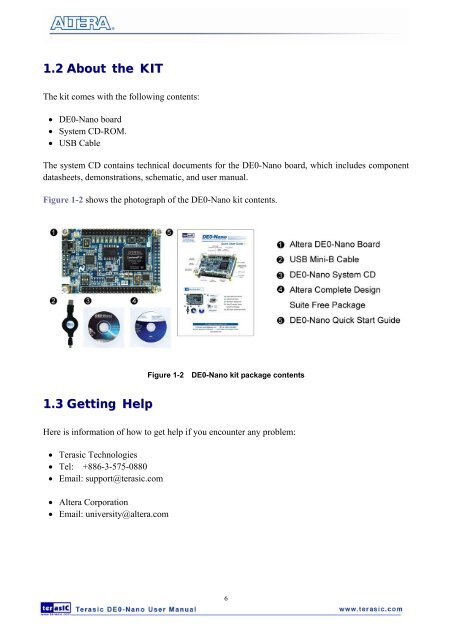
- Page 4 and 5: Chapter 1IntroductionThe DE0-Nano b
- Page 8 and 9: Figure 2-2 The DE0-Nano Board PCB a
- Page 10 and 11: Chapter 3Using the DE0-Nano BoardTh
- Page 15 and 16: DRAM_ADDR[12] PIN_L4 SDRAM Address[
- Page 17 and 18: Figure 3-8 Pin arrangement of the G
- Page 19 and 20: GPIO_17 PIN_T11 GPIO Connection DAT
- Page 21 and 22: Figure 3-12 Pin1 locations of the 2
- Page 23 and 24: Figure 3-14 Block diagram of the cl
- Page 25 and 26: Chapter 4DE0-Nano Control PanelThe
- Page 27 and 28: Figure 4-2 The DE0-Nano Control Pan
- Page 29 and 30: Figure 4-5 Accessing the SDRAMA 16-
- Page 31 and 32: Figure 4-6 Digital Accelerometer st
- Page 33 and 34: Chapter 5DE0-Nano System BuilderThi
- Page 35 and 36: 5.3 Using DE0-Nano System BuilderTh
- Page 37 and 38: • GPIO ExpansionUsers can connect
- Page 39 and 40: Chapter 6Tutorial: Creating an FPGA
- Page 41 and 42: Figure 6-2 Found New Hardware Wizar
- Page 43 and 44: Figure 6-5 Browse to find the locat
- Page 45 and 46: 1. In the Quartus II software, sele
- Page 47 and 48: Figure 6-10 Specify the Device Exam
- Page 51 and 52: Figure 6-14 Saving the Verilog HDL
- Page 53 and 54: 9. Right click in the blank area of
- Page 55 and 56: 3. Click Next.4. In MegaWizard Plug
- Page 57 and 58:
Figure 6-22 MegaWizard Plug-In Mana
- Page 59 and 60:
Figure 6-24 Wizard-Created FilesThe
- Page 61 and 62:
Figure 6-27 Draw a Bus Line connect
- Page 63 and 64:
Figure 6-30 Change the input port n
- Page 65 and 66:
1. Right click in the blank area of
- Page 67 and 68:
Figure 6-35 lpm_mux Symbol13. Click
- Page 69 and 70:
Figure 6-38 Choose output pin18. Cl
- Page 71 and 72:
Figure 6-41 Pin Planner Example2. I
- Page 73 and 74:
Figure 6-43 Default SDCNaming the S
- Page 75 and 76:
Figure 6-45 Compilation Report Exam
- Page 77 and 78:
Figure 6-47 Hardware Setting4. Clic
- Page 79 and 80:
Figure 6-49 Device and OptionsSelec
- Page 81 and 82:
Chapter 7Tutorial: Creating a Nios
- Page 83 and 84:
Figure 7-3 Input the working direct
- Page 85 and 86:
Figure 7-6 New Project Wizard: EDA
- Page 87 and 88:
Figure 7-10 Create New SOPC System
- Page 89 and 90:
Figure 7-14 Add NIOS II Processor89
- Page 91 and 92:
Figure 7-16 Add Nios II CPU complet
- Page 93 and 94:
11. Add a second component by selec
- Page 95 and 96:
Figure 7-21 JTAG UART13. Select the
- Page 97 and 98:
Figure 7-23 Add On-Chip Memory97
- Page 99 and 100:
Figure 7-25 Update Total memory siz
- Page 101 and 102:
Figure 7-28 Update CPU settings101
- Page 103 and 104:
Figure 7-30 Add PIO103
- Page 105 and 106:
Figure 7-32 PIO21. Rename pio_0 to
- Page 107 and 108:
23. Click the Generate button, whic
- Page 109 and 110:
25. Create a new Verilog HDL file,
- Page 111 and 112:
Figure 7-44 and Figure 7-45.module
- Page 113 and 114:
Figure 7-45 DE0_NANO_SOPC module35.
- Page 115 and 116:
37. A dialog box will appear upon s
- Page 117 and 118:
7. Click Change File.8. Browse to t
- Page 119 and 120:
7.4 Create a hello_world Example Pr
- Page 121 and 122:
Figure 7-56 Nios II IDE C++ Project
- Page 123 and 124:
After a successful compilation, rig
- Page 125 and 126:
7.7 Why the LED BlinksThe Nios II s
- Page 127 and 128:
5. Select Run > Resume to resume ex
- Page 129 and 130:
Chapter 8DE0-Nano Demonstrations8.1
- Page 131 and 132:
8.3 ADC ReadingThis demonstration i
- Page 133 and 134:
Figure 8-4 2X13 Header• System Re
- Page 135 and 136:
8.4 SOPC DemoThis demostration illu
- Page 137 and 138:
The data format is configured as 10
- Page 139 and 140:
Demonstration Source Code• Projec
- Page 141 and 142:
8.5 G-SensorThis demonstration illu
- Page 143 and 144:
Chapter 9Appendix9.1 Programming th
- Page 145 and 146:
Figure 9-2 Highlight Flash Loader11
- Page 147 and 148:
Figure 9-4 Convert Programming File
- Page 149 and 150:
2. Program the serial configuration
- Page 151:
9.2 EPCS Programming via nios-2-fla