- Page 4 and 5: Chapter 1IntroductionThe DE0-Nano b
- Page 6: 1.2 About the KITThe kit comes with
- Page 9 and 10: 2.3 Power-up the DE0-Nano BoardThe
- Page 11: Figure 3-1 Programming a serial con
- Page 16 and 17: Figure 3-7 Connections between FPGA
- Page 18 and 19: GPIO_03 PIN_A3 GPIO Connection DATA
- Page 20 and 21: Figure 3-10 Pin distribution of the
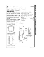
- Page 22 and 23: 3.7 Digital AccelerometerThe ADXL34
- Page 24 and 25: • Power Distribution SystemFigure
- Page 26 and 27: 8. The Control Panel is now ready f
- Page 28 and 29: 4.3 Switches and PushbuttonsChoosin
- Page 30 and 31: The Sequential Read function is use
- Page 32 and 33: 4.7 Overall Structure of the DE0-Na
- Page 34 and 35: The generated system is described u
- Page 36 and 37: Figure 5-3 The DE0-Nano Board Type
- Page 40 and 41: 6.2 Before You BeginThis tutorial a
- Page 42 and 43: The driver is available within the
- Page 44 and 45: The driver will now be installed as
- Page 46 and 47: Figure 6-9 Project informationd. Cl
- Page 48: Figure 6-11 my_first_fpga project6.
- Page 52 and 53: always @ (posedge CLOCK_5)// on pos
- Page 54 and 55: 14. Press the Esc key or click an e
- Page 56 and 57: d. Click Next.Figure 6-21 MegaWizar
- Page 58 and 59: Figure 6-23 MegaWizard Plug-In Mana
- Page 60 and 61: Figure 6-25 PLL Symbol11. Click OK
- Page 62 and 63: 4. Place the new pin onto the BDF s
- Page 64 and 65: Figure 6-31 Change the output BUS n
- Page 66 and 67: Figure 6-34 lpm_mux settings9. Clic
- Page 68 and 69: 15. Add input buses and output pins
- Page 70 and 71: Figure 6-40 Adding the KEY [0] Inpu
- Page 72 and 73: Figure 6-42 Completed Pin Planning
- Page 74 and 75: Figure 6-44 Compilation Message for
- Page 76 and 77: Figure 6-46 Programmer Window2. Cli
- Page 78 and 79: Figure 6-48 Downloading CompleteCon
- Page 80 and 81: Figure 6-50 Setting unused pinsClic
- Page 82 and 83: Figure 7-1 Start to Create a New Pr
- Page 84 and 85: Figure 7-5 New Project Wizard: Fami
- Page 86 and 87: Figure 7-8 A New Complete Project5.
- Page 88 and 89:
Figure 7-12 Create New System[2]7.
- Page 90 and 91:
Figure 7-15 Nios II Processor9. Cli
- Page 92 and 93:
Figure 7-17 Rename the CPU (1)Figur
- Page 94 and 95:
Figure 7-20 JTAG UART’s add wizar
- Page 96 and 97:
Figure 7-22 Rename JTAG UART15. Add
- Page 98 and 99:
Figure 7-24 On-Chip Memory Box16. M
- Page 100 and 101:
Figure 7-26 Add On-Chip memory17. R
- Page 102 and 103:
Figure 7-29 Updated CPU settings19.
- Page 104 and 105:
Figure 7-31 Add PIO20. Click Finish
- Page 106 and 107:
22. Select System > Auto-Assign Bas
- Page 108 and 109:
Figure 7-38 SOPC Builder generation
- Page 110 and 111:
33. Figure 7-42 show a blank Verilo
- Page 112 and 113:
Figure 7-43 Input verilog TextFigur
- Page 114 and 115:
36. Compile the project, by selecti
- Page 116 and 117:
Figure 7-51 Blank Pins39. Input Loc
- Page 118 and 119:
Figure 7-54 Quartus II ProgrammerTh
- Page 120 and 121:
Figure 7-55 Nios II IDE New Project
- Page 122 and 123:
● alt_sys_init.c: an initializati
- Page 124 and 125:
#include "system.h"#include "altera
- Page 126 and 127:
can write to the PIO data register,
- Page 128 and 129:
Figure 7-61 Configuring System Libr
- Page 130 and 131:
Figure 8-2 Pulse Width ModulationFi
- Page 132 and 133:
Table 8-1 DIP Switch SettingsDIP Sw
- Page 134 and 135:
Figure 8-5 ADC Reading hardware set
- Page 136 and 137:
• KEYThe KEY button is driven by
- Page 138 and 139:
Figure 8-11 4-wire SPI Timing Diagr
- Page 140 and 141:
• Input “1” to start Analog t
- Page 142 and 143:
In this demo, the accelerometer is
- Page 144 and 145:
Figure 9-1 Convert Programming File
- Page 146 and 147:
Figure 9-3 Select Devices Page146
- Page 148 and 149:
Figure 9-5 Compression the sof file
- Page 150 and 151:
Figure 9-7 Erasing setting in Quart