User Manual - Terasic
User Manual - Terasic
User Manual - Terasic
- No tags were found...

Create successful ePaper yourself
Turn your PDF publications into a flip-book with our unique Google optimized e-Paper software.
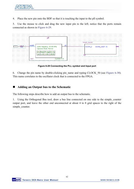
4. Place the new pin onto the BDF so that it is touching the input to the pll symbol.5. Use the mouse to click and drag the new input pin to the left; notice that the ports remainconnected as shown in Figure 6-29.Figure 6-29 Connecting the PLL symbol and Input port6. Change the pin name by double-clicking pin_name and typing CLOCK_50 (see Figure 6-30).This name correlates to the oscillator clock that is connected to the FPGA.• Adding an Output bus to the SchematicThe following steps describe how to add an output bus to the schematic.1. Using the Orthogonal Bus tool, draw a bus line connected on one side to the simple_counteroutput port, and leave the other end unconnected at about 4 to 8 grid spaces to the right of thesimple_counter.62