User Manual - Terasic
User Manual - Terasic
User Manual - Terasic
- No tags were found...

You also want an ePaper? Increase the reach of your titles
YUMPU automatically turns print PDFs into web optimized ePapers that Google loves.
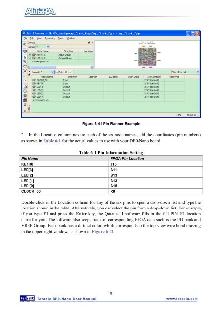
Figure 6-41 Pin Planner Example2. In the Location column next to each of the six node names, add the coordinates (pin numbers)as shown in Table 6-1 for the actual values to use with your DE0-Nano board.Table 6-1 Pin Information SettingPin NameKEY[0]LED[3]LED[2]LED [1]LED [0]CLOCK_50FPGA Pin LocationJ15A11B13A13A15R8Double-click in the Location column for any of the six pins to open a drop-down list and type thelocation shown in the table. Alternatively, you can select the pin from a drop-down list. For example,if you type F1 and press the Enter key, the Quartus II software fills in the full PIN_F1 locationname for you. The software also keeps track of corresponding FPGA data such as the I/O bank andVREF Group. Each bank has a distinct color, which corresponds to the top-view wire bond drawingin the upper right window, as shown in Figure 6-42.71