AV555-PCI-LVDS High Performance Flat Panel/CRT ... - OoCities
AV555-PCI-LVDS High Performance Flat Panel/CRT ... - OoCities
AV555-PCI-LVDS High Performance Flat Panel/CRT ... - OoCities

You also want an ePaper? Increase the reach of your titles
YUMPU automatically turns print PDFs into web optimized ePapers that Google loves.
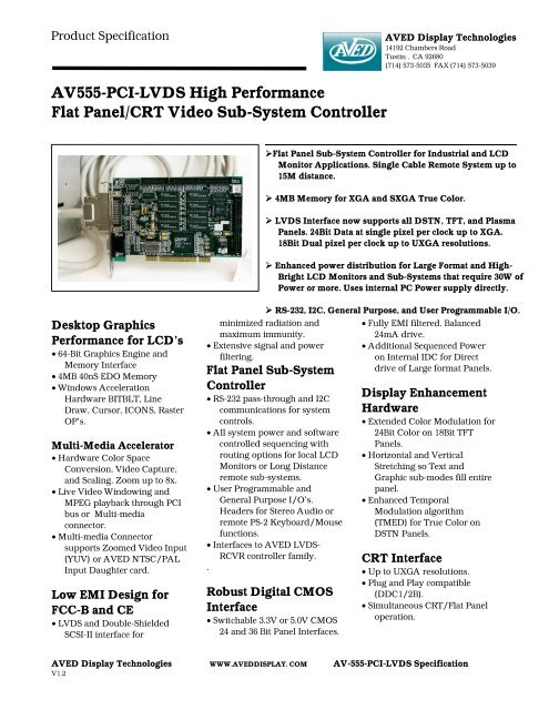
Product SpecificationAVED Display Technologies14192 Chambers RoadTustin , CA 92680(714) 573-5035 FAX (714) 573-5039<strong>AV555</strong>-<strong>PCI</strong>-<strong>LVDS</strong> <strong>High</strong> <strong>Performance</strong><strong>Flat</strong> <strong>Panel</strong>/<strong>CRT</strong> Video Sub-System Controller‣<strong>Flat</strong> <strong>Panel</strong> Sub-System Controller for Industrial and LCDMonitor Applications. Single Cable Remote System up to15M distance.‣ 4MB Memory for XGA and SXGA True Color.‣ <strong>LVDS</strong> Interface now supports all DSTN, TFT, and Plasma<strong>Panel</strong>s. 24Bit Data at single pixel per clock up to XGA.18Bit Dual pixel per clock up to UXGA resolutions.‣ Enhanced power distribution for Large Format and <strong>High</strong>-Bright LCD Monitors and Sub-Systems that require 30W ofPower or more. Uses internal PC Power supply directly.Desktop Graphics<strong>Performance</strong> for LCD’s• 64-Bit Graphics Engine andMemory Interface• 4MB 40nS EDO Memory• Windows AccelerationHardware BITBLT, LineDraw, Cursor, ICONS, RasterOP’s.Multi-Media Accelerator• Hardware Color SpaceConversion, Video Capture,and Scaling. Zoom up to 8x.• Live Video Windowing andMPEG playback through <strong>PCI</strong>bus or Multi-mediaconnector.• Multi-media Connectorsupports Zoomed Video Input(YUV) or AVED NTSC/PALInput Daughter card.Low EMI Design forFCC-B and CE• <strong>LVDS</strong> and Double-ShieldedSCSI-II interface for‣ RS-232, I2C, General Purpose, and User Programmable I/O.minimized radiation andmaximum immunity.• Extensive signal and powerfiltering.<strong>Flat</strong> <strong>Panel</strong> Sub-SystemController• RS-232 pass-through and I2Ccommunications for systemcontrols.• All system power and softwarecontrolled sequencing withrouting options for local LCDMonitors or Long Distanceremote sub-systems.• User Programmable andGeneral Purpose I/O’s.Headers for Stereo Audio orremote PS-2 Keyboard/Mousefunctions.• Interfaces to AVED <strong>LVDS</strong>-RCVR controller family..Robust Digital CMOSInterface• Switchable 3.3V or 5.0V CMOS24 and 36 Bit <strong>Panel</strong> Interfaces.• Fully EMI filtered. Balanced24mA drive.• Additional Sequenced Poweron Internal IDC for Directdrive of Large format <strong>Panel</strong>s.Display EnhancementHardware• Extended Color Modulation for24Bit Color on 18Bit TFT<strong>Panel</strong>s.• Horizontal and VerticalStretching so Text andGraphic sub-modes fill entirepanel.• Enhanced TemporalModulation algorithm(TMED) for True Color onDSTN <strong>Panel</strong>s.<strong>CRT</strong> Interface• Up to UXGA resolutions.• Plug and Play compatible(DDC1/2B).• Simultaneous <strong>CRT</strong>/<strong>Flat</strong> <strong>Panel</strong>operation.AVED Display Technologies WWW.AVEDDISPLAY. COM AV-555-<strong>PCI</strong>-<strong>LVDS</strong> SpecificationV1.2
<strong>High</strong>est QualityStandards• Manufactured to IPC-610-A.Specifications____________________________________Interface SummaryJ1 - 15 Pin <strong>CRT</strong> OutputJ2 - 50 Pin Digital Multi-Media InterfaceJ3 - 24 Bit Digital CMOS <strong>Panel</strong> InterfaceJ4 - 50 Pin External System/<strong>LVDS</strong> InterfaceJ5 - 4 Pin Speaker/User Defined I/OJ6 - 10 Pin RS-232 Pass-Through/I2CJ7 - 4 Pin Auxiliary PC Power InputJ8 - 3 Pin General Purpose I/OJ9 - 3 Pin <strong>LVDS</strong> GPIOTX18/19/20J10 - 20 Pin Auxiliary CMOS <strong>Panel</strong> Interfacefor 36 Bit <strong>Panel</strong>s_____________________________________<strong>CRT</strong> InterfaceAnalog RGB, .7Vptp into 75 Ohms, Nom._____________________________________DDC InterfaceDDC 1/2B compliant on <strong>CRT</strong> and External<strong>Flat</strong> <strong>Panel</strong> Interface. Upgradable to 2B+ forPlug and Display protocol._____________________________________Digital Video <strong>Panel</strong> Interfaces and DataBandwidth24 Bit Digital TTL <strong>Panel</strong> Interface36 Bit Dual Pixel Digital TTL Interface24 Bit <strong>LVDS</strong> Single Pixel Per Clock36 Bit <strong>LVDS</strong> Dual Pixel Per ClockMax Transmission Clock 68MHz. (135MHzBandwidth for Dual Pixel <strong>Panel</strong>s Only).Digital TTL <strong>Panel</strong> Interface voltagesselectable – 3.3V or 5.0V._____________________________________Interface Power/Fuse LimitsFixed +5V 5AFixed +12V 3AFixed -12V 100mASwitched +3.3V 1.2A (VDD)Switched +5V 3A (VDD)Switched +12V 3ANote1: Auxiliary PC Power Connector mustbe connected for Sub-System PowerRequirements over 8W.Note2: Power protected by resettable fuses.If a short condition occurs, wait 5minutes for fuses to reset._____________________________________Video Memory4MB 40nS EDO, 64 Bit Memory Bus_____________________________________Video Modes (<strong>CRT</strong> and TFT LCD)640x480x16M 75Hz800x600x16M 75Hz1024x768x16M 70Hz1280x1024x16M 60Hz1600x1200x256 60HzUp to 135MHz Pixel Clock Rate.Up to 55MHz Memory Clock Rate._____________________________________Control IC’sChips and Technology F65555National DS90C363/TI SN75<strong>LVDS</strong>84_____________________________________Environmental Characteristics•Backed up with 1 year limitedwarranty.• ISO9000 Certification inprocess.Humidity: 5% to 95%, Non-condensing.Ambient Temperature: 0 to 70 C.Operating. -20 to 100 Non-Operating.__________________________________________________________________________EMIFCC Class B and CE for <strong>CRT</strong> InterfaceExternal Digital Sub-System Testsperformed by OEM for System Result.Preliminary Scans pass to FCC-B/CElevels.Internal Ribbon Cable Interface Fully EMIFiltered._____________________________________Power Consumption2.8 W (Board Only)_____________________________________Mechanical DimensionsStandard 32Bit <strong>PCI</strong> Short Card Form Factor(106Hx156Lmm)_____________________________________Software DriversWin3.1, Win95, Win98, NT4.0, OS/2.Available at www.chips.com._____________________________________User Interfaces andConfiguration_____________________________________Jumper SettingsW6 <strong>Panel</strong>/VDDSAFE Voltage Select1-2 +5VOLTS2-3 +3.3VOLTSW7 <strong>Panel</strong> Logic Interface Levels1-2 +5VOLTS2-3 +3.3VOLTS_____________________________________Power Distribution Options For ExternalInterfaceDefault configuration distributes Fixed andSequenced voltages evenly. To supportsub-systems with power consumptionabove 25W alternate configurationshave been designed in.Optionally the External Power Conductorscan be routed to be all Switched Power(for short cables or direct panelinterfacing) or all Fixed Power (for LongDistance Remote Systems that must reregulateand sequence power)._____________________________________I2C Interface ControlI2C Interface implemented withprogrammed I/O and transmittedexternally over twisted pair andinternally on J6. End user must developcommunication program. Test Softwareand Sample Code available fromAVED._____________________________________General Purpose and Programmed I/ORS-232 Pass-Through for Host Systemconnection to Remote System.GPIO1/2 - Hardwire or Logic Controlled.GPIO1 I/O Mapped Control: ConfigWrite 3D0H=0CH, 3D0H=02H. ConfigRead 3D0H=0CH, 3D1H=03H. Operate.Write 3D6=63, Read/Modify Write3D7[1]. GPIO2 is BKLTENABL.SPKR+/-, SPKL+/- Hardwired Audio orGeneral Purpose I/O twisted pairs._____________________________________Ordering InformationPart Number: <strong>AV555</strong>-<strong>LVDS</strong>. Must Specifyany special requirements and <strong>Flat</strong><strong>Panel</strong> vendor and part number.Direct SalesAVED Display Technologies, 14192Chambers Road, Tustin, CA 92780Internet: sales@aveddisplay.com WebSite: www.aveddisplay.com See WebSite for Worldwide Distribution andSales Representatives.U.S. Distribution SalesAll American 800-573-2727Reptron 800- 800-5441Wyle 800-283-9953Technical SupportVisit our Technical Support Center atwww.aveddisplay.com for detailedinstallation guides and manuals.WarrantyAVED Display Technologies (AVED) warrantsthese products to be free from defects inworkmanship and materials under normal use andservice and in its original, unmodified condition,for a period of one year from the time of purchase.All warranties are void if the board isreconfigured or modified without factoryauthorization. If the product is found to bedefective within the terms of this warranty, AVED’ssole responsibility shall be to repair, or at AVED’ssole option, to replace the defective product. Theproduct must be returned by the original customer,insured, and shipped prepaid to AVED. An RMANumber must be obtained from AVED beforethey will be accepted. All replaced productsbecome the sole property of AVED DisplayTechnologies.Copyright NoticeThis document contains information ofproprietary interest to AVED DisplayTechnologies. It has been supplied inconfidence and the recipient, by acceptingthis material, agrees that the subject matterwill not be copied or reproduced, in wholeor in part, nor its contents revealed in anymanner or to any person except to meet thepurpose for which it was delivered.AVED Display Technologies WWW.AVEDDISPLAY. COM AV-555-<strong>PCI</strong>-<strong>LVDS</strong> SpecificationV1.2
Technical data subject to change withoutnotice.“First in Technology,First with Products”Copyright © 1998AVED Display TechnologiesAVED Display Technologies WWW.AVEDDISPLAY. COM AV-555-<strong>PCI</strong>-<strong>LVDS</strong> SpecificationV1.2
<strong>AV555</strong>-<strong>PCI</strong>-<strong>LVDS</strong> Controller Pin Definitions and I/O DescriptionsInternal 50 Pin IDC <strong>Panel</strong> Connector (J3)Description: The Internal 24-Bit Digital CMOS <strong>Panel</strong> Interface. LC filters on clocks and syncs. Ferrites on all data. Mating connector: 50 pin Dual Row .1”IDC. Logic Levels and VDDSAFE are jumper configurable for either 3.3V or 5.0V operation.Pin Signal Pin Signal Pin Signal Pin Signal Pin Signal1 VDDSAFE 11 FLM (VS) 21 P4 31 P11 41 GND2 +12VSAFE 12 GND 22 P5 32 GND 42 P183 +12VSAFE 13 SHFCLK 23 GND 33 P12 43 P194 VDDSAFE 14 GND 24 P6 34 P13 44 GND5 VDDSAFE 15 P0 25 P7 35 GND 45 P206 +12VFUSED 16 P1 26 GND 36 P14 46 P217 GND 17 GND 27 P8 37 P15 47 GND8 M (DE) 18 P2 28 P9 38 GND 48 P229 GND 19 P3 29 GND 39 P16 49 P2310 LP (HS) 20 GND 30 P10 40 P17 50 GNDAuxiliary Internal 20 Pin IDC <strong>Panel</strong> Connector (J10)Description: Auxiliary Color Bits for 36-Bit Digital CMOS Interface. Mating Connector: 20 Pin Dual Row .1” IDC.Pin Signal Pin Signal Pin Signal Pin Signal1 GND 6 P27 11 P30 16 GND2 P24 7 GND 12 P31 17 P343 P25 8 P28 13 GND 18 P354 GND 9 P29 14 P32 19 GND5 P26 10 GND 15 P33 20 GNDExternal 50 Pin <strong>Flat</strong> <strong>Panel</strong>/Sub-System Interface (J3)Description: The External 50 Pin interface for <strong>LVDS</strong> Signals and <strong>Panel</strong> Powers. Designed for use with SCSI-II type connector with Double-ShieldedTwisted Pair cable. Bracketed items indicate alternate multiplexed pin operation – allow customer specific changes. Compatibility Note: This interfaceand connector remain backward compatible with the AVED <strong>LVDS</strong> Receiver boards in addition to Dual 18 Bit TFT’s that have <strong>LVDS</strong> integrated into them.Mating Connector: Male 50 Pin SCSI-II. Board Mount Connector - Amp P/N:AMP 787395-5.Pin Signal Pin Signal Pin Signal Pin Signal Pin Signal1 GND 11 +5VFUSED 21 I2C_SCL (DTR) 31 TXOUT20+ 41 VDDSAFE2 TXOUT10- 12 +12VFUSED 22 GPIO1 (PROGIO1) 32 TXOUT21+ 42 GND3 TXOUT11- 13 GND 23 +5VFUSED 33 TXOUT22+ 43 SDA_RTN/GND (DSR)4 TXOUT12- 14 +12VSAFE 24 SPKR+ 34 TXCLKOUT2+ 44 RTS5 TXCLKOUT1- 15 VDDSAFE 25 SPKL+ 35 GND 45 CTS6 TXOUT20- 16 -12VOLTS 26 GND 36 +12VFUSED 46 SCL_RTN/GND (RI)7 TXOUT21- 17 +12VFUSED 27 TXOUT10+ 37 +12VFUSED 47 GPIO2 (ENABKL)8 TXOUT22- 18 I2C_SDA (DCD) 28 TXOUT11+ 38 GND 48 +5VFUSED9 TXCLKOUT2- 19 RXD 29 TXOUT12+ 39 +12VSAFE 49 SPKR-10 GND 20 TXD 30 TXCLKOUT1+ 40 VDDSAFE 50 SPKL-Internal 50 Pin IDC Multi-Media Interface Connector (J2)Description: Multi-Media Interface Connector for video capture port/daughter card. 16Bit YUV (ZV Video) or RGB Data In. Interface Logic Level are3.3V with 5.0V Tolerant I/O.Pin Signal Pin Signal Pin Signal Pin Signal Pin Signal1 GND 11 VCLK 21 GND 31 SCL 41 GND2 +5VFUSED 12 UV6 (R3) 22 UV1 (G4) 32 Y4 (B4) 42 GND3 GND 13 HREF 23 +12VFUSED 33 GND 43 VREF4 +5VFUSED 14 UV5 (R2) 24 UV0 (G3) 34 Y3 (B3) 44 GND5 GND 15 GND 25 +12VFUSED 35 -12VOLTS 45 GND6 +3.3VOLTS 16 UV4 (R1) 26 Y7 (G2) 36 Y2 (B2) 46 VRDY7 GND 17 GND 27 GND 37 -12VOLTS 47 GND8 +3.3VOLTS 18 UV3 (R0) 28 Y6 (G1) 38 Y1 (B1) 48 GND9 GND 19 GND 29 SDA 39 GND 49 GND10 UV7 (R4) 20 UV2 (G5) 30 Y5 (G0) 40 Y0 (B0) 50 GNDAVED Display Technologies WWW.AVEDDISPLAY. COM AV-555-<strong>PCI</strong>-<strong>LVDS</strong> Specification V1.2
<strong>AV555</strong>-<strong>PCI</strong>-<strong>LVDS</strong> Controller Pin Definitions and I/O Descriptions (cont.)10 Pin RS-232 (J6)Description: The 10 Pin RS-232 Pass-Through connector. Standard PC“AT” connector arrangement and definitions. Note that the defaultconfiguration uses DCD, DSR, DTR, RI for I2C interface to external I/O(J4) and must be left disconnected when resistors () are installed. Note:Typical Serial Communications devices such as a mouse or touch-screencontroller only require RXD, TXD, RTS, CTS. . Routed to J3 ExternalInterface.Pin Signal1 DCD (I2C_SDA)(R11)2 DSR (SDA_RTN)(R12)3 RXD4 RTS5 TXD6 CTS7 DTR (I2C_SCL) (R13)8 RI (SCL_RTN) (R14)9 GND10 NC4 Pin Speaker/User Defined I/O Twisted Pair (J5)Description: Hardwired General purpose I/O suitable for <strong>High</strong> LevelAudio, PS-2 Keyboard/Mouse, power, or whatever. SPKR+/- andSPKL+/- are run as twisted pairs over the external interface. Routed to J3External Interface. Mating connector: 4 pin Single .1” IDC.Pin Signal1 SPKR+2 SPKR-3 SPKL-4 SPKL+3 Pin General Purpose I/O (J8)Description: Hardwired General purpose I/O limited to 5V max.External logic to over-drive 4.7K pull-up. Logic Controlled I/O are alsoconnected: 1. GPIO1 connects to user I/O programmable signal (seeabove section for programming), GPIO2 connect to ENABKL which isactive high Backlight Enable signal. . Routed to J3 External Interface.Pin Signal1 GPIO12 GPIO23 GNDAuxiliary Power Input Connector (J7)Description: Power Input from Standard PC Power Supply. Alwaysconnect when using <strong>Flat</strong> <strong>Panel</strong> or Sub-Systems that consume more than 8Watts.Pin Signal1 +5VOLTS2 GND3 GND4 +12VOLTSKey Improvements for AV-555-<strong>PCI</strong>-<strong>LVDS</strong> over the AV-550-<strong>PCI</strong>-<strong>LVDS</strong>1. 4MB Memory translates to XGA and SXGA True Color. The 64 Bit HiQVideo Hardware Graphics Controller alongwith a 64 Bit Memory Bus make this the highest performance AVED Video Controller.2. <strong>LVDS</strong> Interface now supports all DSTN and TFT <strong>Panel</strong> Interfaces. 24 Bit Data at single pixel per clock is nowsupported up to XGA resolutions. Dual pixel per clock supported up to UXGA resolutions.3. Enhanced power distribution for Large Format and <strong>High</strong>-Bright LCD Monitors and Sub-Systems that require 30W ofpower or more. Can use internal PC Power supply directly. Board power routing options for local LCD Monitors orLong Distance remote sub-systems.4. Fully Buffered and EMI filtered Digital CMOS Interfaces. For “Internal” ribbon cable connections up to 36 bits wide.<strong>High</strong> (24mA) Drive allow direct “External” Digital Interfaces as well. In fact, internal CMOS, external <strong>LVDS</strong>, and<strong>CRT</strong> interfaces can all be run simultaneously assuming the same panel type.5. All fixed and programmable powers supplies protected by automatically resettable fuses. Avoids field failures whena momentary short occurs. System will resume once cause of continuous over-current condition is resolved.6. User programmable I2C capability added to External Interface. OEM application and control software cancommunicate with external sub-system.7. Setting for <strong>LVDS</strong> <strong>Panel</strong> Types DSTN or TFT as well as clock polarity are controlled by the software video BIOS. Aminimum of user configurable jumpers.AVED Display Technologies WWW.AVEDDISPLAY. COM AV-555-<strong>PCI</strong>-<strong>LVDS</strong> Specification V1.2
<strong>AV555</strong>-<strong>PCI</strong>-<strong>LVDS</strong> Internal Digital CMOS <strong>Panel</strong> Interface DefinitionDescription: Selectable 3.3V or 5.0V logic levels. Fully EMI Filtered. Compatibility Note: Internal 50 Pin IDC (J3) is backwards compatible with all otherAVED products. Additional 20 Pin IDC (J10) is a new definition and is required for Dual Pixel Per Clock <strong>Panel</strong> Interfaces. All cable lengths should bekept to a minimum and the maximum amount of grounds from the board carried across to the panel should always be used.Signal Name <strong>AV555</strong>Internal 50 PinIDC - J3+5VOLT NCFUSEDVDDSAFE 1,4,5+12VSAFE 2,3+12 V FUSED 6<strong>AV555</strong> Internal20 Pin IDC, J1024 Bit TFTSingle Pixel/Clock36 bit TFTDual Pixel/Clock12 Bit TFTDual Pixel/Clock24 Bit ColorDSTN16 Bit ColorDSTNM (DE) 8LP (HS) 10FLM (VS) 11SHFCLK 13P0 15 B0 FB0 FB0 UR0 UR0P1 16 B1 FB1 FB1 UG0 UG0P2 18 B2 FB2 FB2 UB0 UB0P3 19 B3 FB3 FB3 LR0 UR1P4 21 B4 FB4 SB0 LG0 LR0P5 22 B5 FB5 SB1 LB0 LG0P6 24 B6 SB0 SB2 UR1 LB0P7 25 B7 SB1 SB3 UG1 LR1P8 27 G0 SB2 FG0 UB1 UG1P9 28 G1 SB3 FG1 LR1 UB1P10 30 G2 SB4 FG2 LG1 UR2P11 31 G3 SB5 FG3 LB1 UG2P12 33 G4 FG0 SGO UR2 LG1P13 34 G5 FG1 SG1 UG2 LB1P14 36 G6 FG2 SG2 UB2 LR2P15 37 G7 FG3 SG3 LR2 LG2P16 39 R0 FG4 FR0 LG2P17 40 R1 FG5 FR1 LB2P18 42 R2 SG0 FR2 UR3P19 43 R3 SG1 FR3 UG3P20 45 R4 SG2 SR0 UB3P21 46 R5 SG3 SR1 LR3P22 48 R6 SG4 SR2 LG3P23 49 R7 SG5 SR3 LB3P24 2 FR0P25 3 FR1P26 5 FR2P27 6 FR3P28 8 FR4P29 9 FR5P30 11 SR0P31 12 SR1P32 14 SR2P33 15 SR3P34 17 SR4P35 18 SR5GND 7,9,12,14,17,20,23,26,29,32,35,38,41,44,47, 501,4,7,10,13,16,19,20AVED Display Technologies WWW.AVEDDISPLAY. COM AV-555-<strong>PCI</strong>-<strong>LVDS</strong> Specification V1.2
<strong>AV555</strong>-<strong>PCI</strong>-<strong>LVDS</strong> <strong>LVDS</strong> Signal MappingDescription: The following table describes the mapping between the <strong>LVDS</strong> Transmission Lines and the organization of interface signal thatdrive the <strong>LVDS</strong> IC’s before they are combined into serial transmission line data. Two discrete 18 Bit <strong>LVDS</strong> IC’s are used to support all panelinterface types. The most common supported panel interfaces are: Dual Pixel/Clock 18 Bit TFT, Single Pixel/Clock 24 Bit TFT, 24 Bit ColorDSTN, 18 Bit Color DSTN.36 Bit Dual-Pixel/Clock(Industry Standard for XGA andSXGA TFT <strong>LVDS</strong> Interfaces)24 Bit SinglePixel/Clock24 Bit Color DSTN 18 Bit Color DSTNTXOUT1X DefinitionsTXIN0 First RED 0 - - -TXIN1 First RED 1 Blue 0 UR0 UR0TXIN2 First RED 2 - - -TXIN3 First RED 3 - - -TXIN4 First RED 4 - - -TXIN5 First RED 5 - - -TXIN6 First Green 0 Green 4 UR2 LG1TXIN7 First Green 1 Green 5 UG2 LB1TXIN8 First Green 2 Green 6 UB2 LR2TXIN9 First Green 3 Green 7 LR2 LG2TXIN10 First Green 4 Red 0 LG2 -TXIN11 First Green 5 Red 1 LB2 -TXIN12 First Blue 0 NC (Blue 0) Don’t Use - -TXIN13 First Blue 1 Blue 1 UG0 UG0TXIN14 First Blue 2 Blue 2 UB0 UB0TXIN15 First Blue 3 Blue 3 LR0 UR1TXIN16 First Blue 4 Blue 4 LG0 LR0TXIN17 First Blue 5 Blue 5 LB0 LG0TXIN18 HSYNC HSYNC LP LPTXIN19 VSYNC VSYNC FLM FLMTXIN20 DE DE M MTXCLKIN SHFCLK (Pixel Clock/2) SHFCLK (Pixel Clock) Pixel Clock Pixel ClockTXOUT2X DefinitionsTXIN0 Second RED 0 - <strong>Panel</strong> Data Clock <strong>Panel</strong> Data ClockTXIN1 Second RED 1 - - -TXIN2 Second RED 2 - - -TXIN3 Second RED 3 - - -TXIN4 Second RED 4 - - -TXIN5 Second RED 5 - - -TXIN6 Second Green 0 Red 2 UR3 -TXIN7 Second Green 1 Red 3 UG3 -TXIN8 Second Green 2 Red 4 UB3 -TXIN9 Second Green 3 Red 5 LR3 -TXIN10 Second Green 4 Red 6 LG3 -TXIN11 Second Green 5 Red 7 LB3 -TXIN12 Second Blue 0 Blue 6 UR1 LB0TXIN13 Second Blue 1 Blue 7 UG1 LR1TXIN14 Second Blue 2 Green 0 UB1 UG1TXIN15 Second Blue 3 Green 1 LR1 UB1TXIN16 Second Blue 4 Green 2 LG1 UR2TXIN17 Second Blue 5 Green 3 LB1 UG2TXIN18 Pull Down/ J9-1 GPIO/ENABKL Same Same SameTXIN19 Pull Down/J9-2 GPIO/GPIO1 Same Same SameTXIN20 Pull Down/J9-3 GPIO Same Same SameTXCLKIN SHFCLK (Pixel Clock/2) SHFCLK (Pixel Clock) Pixel Clock Pixel ClockAVED Display Technologies WWW.AVEDDISPLAY. COM AV-555-<strong>PCI</strong>-<strong>LVDS</strong> SpecificationV1.2