SN74LS122, SN74LS123 Retriggerable Monostable Multivibrators
SN74LS122, SN74LS123 Retriggerable Monostable Multivibrators
SN74LS122, SN74LS123 Retriggerable Monostable Multivibrators
- No tags were found...

You also want an ePaper? Increase the reach of your titles
YUMPU automatically turns print PDFs into web optimized ePapers that Google loves.
These dc triggered multivibrators feature pulse width control bythree methods. The basic pulse width is programmed by selection ofexternal resistance and capacitance values. The LS122 has an internaltiming resistor that allows the circuits to be used with only an externalcapacitor. Once triggered, the basic pulse width may be extended byretriggering the gated low-level-active (A) or high-level-active (B)inputs, or be reduced by use of the overriding clear.• Overriding Clear Terminates Output Pulse• Compensated for VCC and Temperature Variations• DC Triggered from Active-High or Active-Low Gated Logic Inputs• <strong>Retriggerable</strong> for Very Long Output Pulses, up to 100% Duty Cycle• Internal Timing Resistors on LS122GUARANTEED OPERATING RANGESSymbol Parameter Min Typ Max UnitVCC Supply Voltage 4.75 5.0 5.25 VTAOperating AmbientTemperature Range0 25 70 °CIOH Output Current – High –0.4 mAIOL Output Current – Low 8.0 mARext External Timing Resistance 5.0 260 kCext External Capacitance No RestrictionRext/CextWiring Capacitance atRext/Cext Terminal50 pF1416LOW POWER SCHOTTKY11161416http://onsemi.com111PLASTICN SUFFIXCASE 646SOICD SUFFIXCASE 751APLASTICN SUFFIXCASE 648SOICD SUFFIXCASE 751BSOEIAJM SUFFIXCASE 966ORDERING INFORMATIONDevice Package Shipping<strong>SN74LS122</strong>N 14 Pin DIP 2000 Units/Box<strong>SN74LS122</strong>D SOIC–14 55 Units/Rail<strong>SN74LS122</strong>DR2 SOIC–14 2500/Tape & Reel<strong>SN74LS123</strong>N 16 Pin DIP 2000 Units/Box<strong>SN74LS123</strong>D SOIC–16 38 Units/Rail<strong>SN74LS123</strong>DR2 SOIC–16 2500/Tape & Reel<strong>SN74LS123</strong>M SOEIAJ–16 See Note 1<strong>SN74LS123</strong>MEL SOEIAJ–16 See Note 11. For ordering information on the EIAJ version ofthe SOIC package, please contact your localON Semiconductor representative.© Semiconductor Components Industries, LLC, 2001October, 2001 – Rev. 71 Publication Order Number:<strong>SN74LS122</strong>/D
<strong>SN74LS122</strong>, <strong>SN74LS123</strong><strong>SN74LS123</strong> (TOP VIEW)(SEE NOTES 1 THRU 4) <strong>SN74LS122</strong> (TOP VIEW)(SEE NOTES 1 THRU 4) http://onsemi.com2
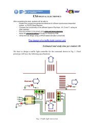
<strong>SN74LS122</strong>, <strong>SN74LS123</strong>WAVEFORMSRETRIGGERPULSE(See Application Data)B INPUTQ OUTPUTOUTPUT WITHOUT RETRIGGEREXTENDING PULSE WIDTHB INPUTCLEAR INPUTCLEAR PULSEQ OUTPUTOUTPUT WITHOUT CLEAR PULSEOVERRIDING THE OUTPUT PULSEhttp://onsemi.com4
<strong>SN74LS122</strong>, <strong>SN74LS123</strong>DC CHARACTERISTICS OVER OPERATING TEMPERATURE RANGE (unless otherwise specified)LimitsSymbol Parameter Min Typ Max Unit Test ConditionsVIH Input HIGH Voltage 2.0 VGuaranteed Input HIGH Voltage forAll InputsVILInput LOW Voltage0.8VGuaranteed Input LOW Voltage forAll InputsVIK Input Clamp Diode Voltage –0.65 –1.5 V VCC = MIN, IIN = –18 mAVOHOutput HIGH Voltage2.7 3.5 V VCC = MIN, IOH = MAX, VIN = VIHor VIL per Truth TableVOLOutput LOW Voltage0.25 0.4 V IOL = 4.0 mA VCC = VCC MIN,VIN = VIL or VIH0.35 0.5 V IOL = 8.0 mA per Truth TableIIHInput HIGH Current20 µA VCC = MAX, VIN = 2.7 V0.1 mA VCC = MAX, VIN = 7.0 VIIL Input LOW Current –0.4 mA VCC = MAX, VIN = 0.4 VIOS Short Circuit Current (Note 2) –20 –100 mA VCC = MAXLS122 11ICCPower Supply CurrentLS123 20mAVCC = MAX2. Not more than one output should be shorted at a time, nor for more than 1 second.AC CHARACTERISTICS (TA = 25°C, VCC = 5.0 V)LimitsSymbol Parameter Min Typ Max Unit Test ConditionsPropagation 23 33tPLHDelay, A to QtPHL Propagation Delay, A to Q 32 45Propagation 23 44tPLHDelay, B to QtPHL Propagation Delay, B to Q 34 56Propagation 28 45tPLHDelay, Clear to QtPHL Propagation Delay, Clear to Q 20 27nsnsnsCext = 0CL = 15 pFRext = 5.0 kΩRL = 2.0 kΩtW min A or B to Q 116 200 ns Cext = 1000 pF, Rext = 10 kΩ,tWQ A to B to Q 4.0 4.5 5.0 µs CL = 15 pF, RL = 2.0 kΩAC SETUP REQUIREMENTS (TA = 25°C, VCC = 5.0 V)LimitsSymbol Parameter Min Typ Max Unit Test ConditionstW Pulse Width 40 nshttp://onsemi.com5
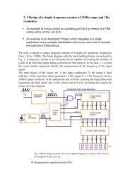
<strong>SN74LS122</strong>, <strong>SN74LS123</strong>VCCVRCRextVCCVCC VRC VCCRextPin51 ΩCextCext Rext/ VCCCext QCLR1/2 LS123BAGNDQ0.1 µFPoutPin51 ΩCextCLRB2B1A2A1CextRext/CextLS122GNDVCCQQ0.1 µFPoutFigure 1. Figure 2.PinPouttWFigure 3.RETRIGGER105K ≤ Rext ≤ 260K µ0.10.0110.0010.3 0.35 0.4 0.45 0.5 0.55KFigure 4.http://onsemi.com6
<strong>SN74LS122</strong>, <strong>SN74LS123</strong>0.55VRC = 5 VCext = 1000 pF0.55VCC = 5 VCext = 1000 pF0.55Cext = 1000 pF0.5K0.450.4°°°°°0.5K0.450.4° °°°°0.5K0.450.4°°°°°0.354.5 5 5.5VCC0.354.5 5 5.5VRC0.354.5 5 5.5VCC = VRCFigure 5. K versus VCC Figure 6. K versus VRC Figure 7. K versus VCC and VRC100000, OUTPUT PULSE WIDTH (ns)tW100001000Rext = 260 kΩRext = 160 kΩ100Rext = 80 kΩRext = 40 kΩRext = 20 kΩRext = 10 kΩRext = 5 kΩ101 10 100 1000Cext, EXTERNAL TIMING CAPACITANCE (pF)Figure 8.http://onsemi.com7
<strong>SN74LS122</strong>, <strong>SN74LS123</strong>0.65Cext = 200 pF°0.6°°K 0.55°°0.54.5 4.75 5 5.25 5.5VCC VOLTSFigure 9.VCCPIN 7OR 15RextRextREMOTECextPIN 6OR 14Figure 10. LS123 Remote Trimming Circuithttp://onsemi.com8
<strong>SN74LS122</strong>, <strong>SN74LS123</strong>VCCPIN 9PIN 13OPENRextRextREMOTECextPIN 11Figure 11. LS122 Remote Trimming Circuit Without RextVCCPIN 9RextREMOTEPIN 13PIN 11Figure 12. LS122 Remote Trimming Circuit with Rinthttp://onsemi.com9
<strong>SN74LS122</strong>, <strong>SN74LS123</strong>PACKAGE DIMENSIONSBN SUFFIXPLASTIC PACKAGECASE 646–06ISSUE M –T–NA FL C K J H G D 14 PLM –A––B–P 7 PLD SUFFIXPLASTIC SOIC PACKAGECASE 751A–03ISSUE F –T–GD 14 PL K C R X 45 F MJ http://onsemi.com10
<strong>SN74LS122</strong>, <strong>SN74LS123</strong>PACKAGE DIMENSIONSN SUFFIXPLASTIC PACKAGECASE 648–08ISSUE RH–A–GBFCSKD 16 PL –T– JLM D SUFFIXPLASTIC SOIC PACKAGECASE 751B–05ISSUE J–T–G–A–D 16 PL K –B– P 8 PL R X 45CM JF http://onsemi.com11
<strong>SN74LS122</strong>, <strong>SN74LS123</strong>PACKAGE DIMENSIONSM SUFFIXSOEIAJ PACKAGECASE 966–01ISSUE OeZDb LEE HE M VIEW PAA1LDETAIL PQ1c ON Semiconductor and are trademarks of Semiconductor Components Industries, LLC (SCILLC). SCILLC reserves the right to make changeswithout further notice to any products herein. SCILLC makes no warranty, representation or guarantee regarding the suitability of its products for any particularpurpose, nor does SCILLC assume any liability arising out of the application or use of any product or circuit, and specifically disclaims any and all liability,including without limitation special, consequential or incidental damages. “Typical” parameters which may be provided in SCILLC data sheets and/orspecifications can and do vary in different applications and actual performance may vary over time. All operating parameters, including “Typicals” must bevalidated for each customer application by customer’s technical experts. SCILLC does not convey any license under its patent rights nor the rights of others.SCILLC products are not designed, intended, or authorized for use as components in systems intended for surgical implant into the body, or other applicationsintended to support or sustain life, or for any other application in which the failure of the SCILLC product could create a situation where personal injury ordeath may occur. Should Buyer purchase or use SCILLC products for any such unintended or unauthorized application, Buyer shall indemnify and holdSCILLC and its officers, employees, subsidiaries, affiliates, and distributors harmless against all claims, costs, damages, and expenses, and reasonableattorney fees arising out of, directly or indirectly, any claim of personal injury or death associated with such unintended or unauthorized use, even if such claimalleges that SCILLC was negligent regarding the design or manufacture of the part. SCILLC is an Equal Opportunity/Affirmative Action Employer.PUBLICATION ORDERING INFORMATIONLiterature Fulfillment:Literature Distribution Center for ON SemiconductorP.O. Box 5163, Denver, Colorado 80217 USAPhone: 303–675–2175 or 800–344–3860 Toll Free USA/CanadaFax: 303–675–2176 or 800–344–3867 Toll Free USA/CanadaEmail: ONlit@hibbertco.comN. American Technical Support: 800–282–9855 Toll Free USA/CanadaJAPAN: ON Semiconductor, Japan Customer Focus Center4–32–1 Nishi–Gotanda, Shinagawa–ku, Tokyo, Japan 141–0031Phone: 81–3–5740–2700Email: r14525@onsemi.comON Semiconductor Website: http://onsemi.comFor additional information, please contact your localSales Representative.http://onsemi.com12<strong>SN74LS122</strong>/D