Minimum 3: Implementing FSM in VHDL and simulations in Quartus-II
Minimum 3: Implementing FSM in VHDL and simulations in Quartus-II
Minimum 3: Implementing FSM in VHDL and simulations in Quartus-II

Create successful ePaper yourself
Turn your PDF publications into a flip-book with our unique Google optimized e-Paper software.
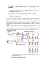
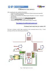
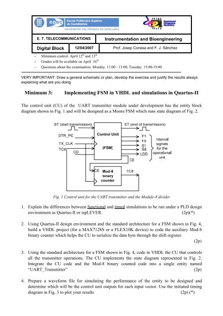
E. T. TELECOMMUNICATIONS Instrumentation <strong>and</strong> Bioeng<strong>in</strong>eer<strong>in</strong>gDigital Block 12/04/2007 Prof. Josep Conesa <strong>and</strong> F. J. Sànchez- <strong>M<strong>in</strong>imum</strong> control: April 12 th <strong>and</strong> 13 th- Grades will be available on April 16 th- Questions about the exam<strong>in</strong>ation: Monday 11:00 - 13:00; Tuesday 15:00-19:00VERY IMPORTANT: Draw a general schematic or plan, develop the exercise <strong>and</strong> justify the results alwaysexpla<strong>in</strong><strong>in</strong>g what are you do<strong>in</strong>g<strong>M<strong>in</strong>imum</strong> 3:<strong>Implement<strong>in</strong>g</strong> <strong>FSM</strong> <strong>in</strong> <strong>VHDL</strong> <strong>and</strong> <strong>simulations</strong> <strong>in</strong> <strong>Quartus</strong>-<strong>II</strong>The control unit (CU) of the UART transmitter module under development has the entity blockdiagram shown <strong>in</strong> Fig. 1 <strong>and</strong> will be designed as a Moore <strong>FSM</strong> which runs state diagram of Fig. 2.Fig. 1 Control unit for the UART transmitter <strong>and</strong> the Module-8 divider1. Expla<strong>in</strong> the differences between functional <strong>and</strong> timed <strong>simulations</strong> to be run under a PLD designenvironment as <strong>Quartus</strong>-<strong>II</strong> or ispLEVER.(2p)(*)2. Us<strong>in</strong>g <strong>Quartus</strong>-<strong>II</strong> design environment <strong>and</strong> the st<strong>and</strong>ard architecture for a <strong>FSM</strong> shown <strong>in</strong> Fig. 4,build a <strong>VHDL</strong> project (for a MAX7128S or a FLEX10K device) to code the auxiliary Mod-8b<strong>in</strong>ary counter which helps the CU to serialize the data byte through the shift register.(2p)3. Us<strong>in</strong>g the st<strong>and</strong>ard architecture for a <strong>FSM</strong> shown <strong>in</strong> Fig. 4, code <strong>in</strong> <strong>VHDL</strong> the CU that controlsall the transmitter operations. The CU implements the state diagram represented <strong>in</strong> Fig. 2.Integrate the CU code <strong>and</strong> the Mod-8 b<strong>in</strong>ary counted code <strong>in</strong>to a s<strong>in</strong>gle entity named“UART_Transmitter”(2p)4. Prepare a waveform file for simulat<strong>in</strong>g the performance of the entity to be designed <strong>and</strong>determ<strong>in</strong>e which will be the control unit outputs for each <strong>in</strong>put vector. Use the <strong>in</strong>itiated tim<strong>in</strong>gdiagram <strong>in</strong> Fig. 3 to plot your results (2p) (*)
5. Verify the “UART_Transmitter” entity operation through a functional <strong>and</strong> a timed simulation.Determ<strong>in</strong>e the worse case propagation delay <strong>and</strong> the maximum frequency of operation for thecircuit attend<strong>in</strong>g the results of the “tim<strong>in</strong>g analysis”.(2p)6. (For students who want to go further <strong>in</strong> EX3) Complete the <strong>Quartus</strong>-<strong>II</strong> design flow (p<strong>in</strong>assignment <strong>and</strong> device programm<strong>in</strong>g) to implement your design <strong>in</strong> the Altera UP2 tra<strong>in</strong><strong>in</strong>gboard. Integrate the operational unit blocs (multiplexer, parity generator, registers, quartz clockdividers <strong>and</strong> debounc<strong>in</strong>g circuit) <strong>in</strong> your “UART_Transmitter” project as stated <strong>in</strong> EX3.Fig. 2 <strong>FSM</strong> state diagram
Fig. 3 Sketch of an <strong>in</strong>itial tim<strong>in</strong>g diagram to be developed for predict<strong>in</strong>g <strong>and</strong> simulat<strong>in</strong>g theoutput waveforms
Us<strong>in</strong>g concurrent assignments orsignal-sensitive processesrCOMBINATIONALSYSTEMCS2mZ (outputs)Xn(<strong>in</strong>puts)rrCOMBINACIONALSYSTEMCS1future_stateSIGNALSSTATE MEMORYCLKUsually us<strong>in</strong>g FF-DCDpresent_staterState_register (Clock <strong>and</strong> CDsensitive processFig. 4 Example diagram to represent the ma<strong>in</strong> blocks <strong>in</strong> the <strong>VHDL</strong> code (the number of bits rnecessary to code the <strong>in</strong>ternal state will depend on the cod<strong>in</strong>g strategy (b<strong>in</strong>ary, Gray, oneshot,etc.)