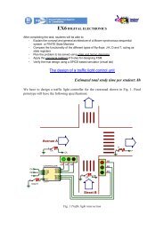
2. 5 Design of a simple frequency counter of 1MHz range and 1Hz ...
2. 5 Design of a simple frequency counter of 1MHz range and 1Hz ...
2. 5 Design of a simple frequency counter of 1MHz range and 1Hz ...

Create successful ePaper yourself
Turn your PDF publications into a flip-book with our unique Google optimized e-Paper software.
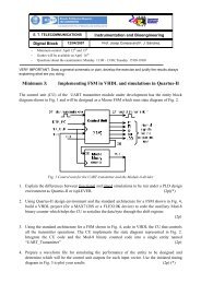
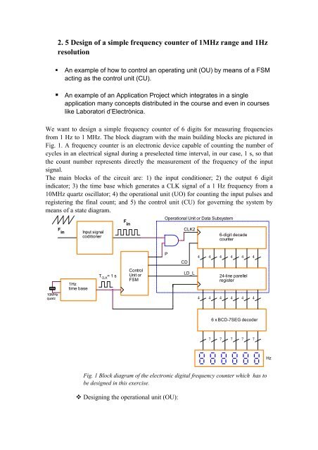
<strong>2.</strong> 5 <strong>Design</strong> <strong>of</strong> a <strong>simple</strong> <strong>frequency</strong> <strong>counter</strong> <strong>of</strong> <strong>1MHz</strong> <strong>range</strong> <strong>and</strong> <strong>1Hz</strong>resolution• An example <strong>of</strong> how to control an operating unit (OU) by means <strong>of</strong> a FSMacting as the control unit (CU).• An example <strong>of</strong> an Application Project which integrates in a singleapplication many concepts distributed in the course <strong>and</strong> even in courseslike Laboratori d’Electrònica.We want to design a <strong>simple</strong> <strong>frequency</strong> <strong>counter</strong> <strong>of</strong> 6 digits for measuring frequenciesfrom 1 Hz to 1 MHz. The block diagram with the main building blocks are pictured inFig. 1. A <strong>frequency</strong> <strong>counter</strong> is an electronic device capable <strong>of</strong> counting the number <strong>of</strong>cycles in an electrical signal during a preselected time interval, in our case, 1 s, so thatthe count number represents directly the measurement <strong>of</strong> the <strong>frequency</strong> <strong>of</strong> the inputsignal.The main blocks <strong>of</strong> the circuit are: 1) the input conditioner; 2) the output 6 digitindicator; 3) the time base which generates a CLK signal <strong>of</strong> a 1 Hz <strong>frequency</strong> from a10MHz quartz oscillator; 4) the operational unit (UO) for counting the input pulses <strong>and</strong>registering the final count; <strong>and</strong> 5) the control unit (CU) for governing the system bymeans <strong>of</strong> a state diagram.FinInput signalcoditionerFinOperational Unit or Data SubsystemCLK26-digit decade<strong>counter</strong>ControlLD_LTCLK= 1 s Unit or24-line parellelFSMregister<strong>1Hz</strong>time base10MHzquarz 4 4 4 4 4PCD44444446 x BCD-7SEG decoder77777HzFig. 1 Block diagram <strong>of</strong> the electronic digital <strong>frequency</strong> <strong>counter</strong> which has tobe designed in this exercise. <strong>Design</strong>ing the operational unit (OU):
- Implement the <strong>counter</strong> module 10 6 for having a measurement <strong>range</strong> <strong>of</strong> 6 digits.Use a chain <strong>of</strong> 6 decade <strong>counter</strong>s, which can be, for example, the universal<strong>counter</strong>s implemented in Problem <strong>2.</strong>13 truncated for a BCD count).- Implement the 24 bit parallel register for saving the <strong>frequency</strong> count. Use, forexample, the parallel load feature <strong>of</strong> an universal <strong>counter</strong> which has beenpermanently disabled for counting (CE_L = 1). <strong>Design</strong>ing the output module for the 7-segment displays:- Use <strong>and</strong> adapt the circuit designed in Problem 1.8 for this task.DCBABI_LLT_LRBI_LSCa_Lb_Lc_Ld_Le_Lf_Lg_LRBO_LDESCODIFICADOR HEX-7SEG <strong>Design</strong>ing the input signal conditioner for adapting many waveforms <strong>and</strong>voltages <strong>range</strong>s.- In this case, you have to rely on the concepts <strong>and</strong> circuits implemented in theLaboratori d’Electrònica course. Try for example, an operational amplifierconnected in open loop acting as comparator in order to obtain a digital squarewaveform from a sinusoidal input. <strong>Design</strong>ing the control unita) Specifications: Symbol: Shown in Fig. 1. Example <strong>of</strong> a timing diagram showing the CLK signal, <strong>and</strong> the output’sactivity for some periods. State diagramb) Particularize the general architecture <strong>of</strong> a Moore FSM to the problem as in Fig.2 if FF-JK (use for example the 74112) are selected as the state memory buildingblock.
Q[1..0]SC2PCDLD_LSC14CLKStatememory2Q[1..0]Fig. 2 Example <strong>of</strong> particularization <strong>of</strong> the canonical FSM that can be designedstep by step following the general procedure stated in Unit <strong>2.</strong>5.c) Codify the states in binary code.d) Draw the state memory schematic.e) <strong>Design</strong> the SC2, which produces the outputs CD, LD_L, <strong>and</strong> P.f) <strong>Design</strong> the SC1, which establishes the next state after each CLK edge transitionfrom low to high.g) (optional) Capture the schematics in Proteus-VSM Lite <strong>and</strong> perform a circuitsimulation to verify if the design follows the specifications stated in a).h) (optional) Using the MAX-PLUS s<strong>of</strong>tware from Altera, try to capture theschematics or VHDL files for describing de circuit <strong>and</strong> program a CPLD likeMAX7128 or FLEX10K to implement the whole circuit in a single chip.