- Page 1 and 2: SDVD001. LSI LogicData Book1986~TEX
- Page 4 and 5: LSI Logic Data BookTEXASINSTRUMENTS
- Page 6: INTRODUCTIONThe LSI Logic Data Book
- Page 9 and 10: 1-2
- Page 11 and 12: C)CD:sCD!. "":s .....o""3Q)r+o·:s1
- Page 13 and 14: GLOSSARYTTL SYMBOLS, TERMS, AND DEF
- Page 15 and 16: GLOSSARYTTL SYMBOLS, TERMS, AND DEF
- Page 17 and 18: EXPLANATION OF FUNCTION TABLESAmong
- Page 19 and 20: 1-12
- Page 21 and 22: FUNCTIONAL INDEXGATES, EXPANDERS, B
- Page 23 and 24: FUNCTIONAL. INDEXBUFFERS, DRIVERS,
- Page 25 and 26: FUNCTIONAL INDEXLATCHES AND MUL TIV
- Page 27 and 28: FUNCTIONAL INDEXCOUNTERSSYNCHRONOUS
- Page 29 and 30: FUNCTIONAL INDEXDISPLAY DECODERS/DR
- Page 31 and 32: FUNCTIONAL INDEXARITHMETIC CIRCUITS
- Page 33 and 34: FUNCTIONAL INDEXPROGRAMMABLE LOGIC
- Page 35 and 36: (J)cCD
- Page 37 and 38: SN54AS181A, SN54AS881A, SN74AS181A,
- Page 39 and 40: SN54AS181A, SN54AS881A, SN74AS181A,
- Page 41 and 42: SN54AS881A, SN74AS881AARITHMETIC LO
- Page 43 and 44: SN54AS181A, SN54AS881A, SN74AS181A,
- Page 45: SN54AS181A, SN54AS881A, SN74AS181A,
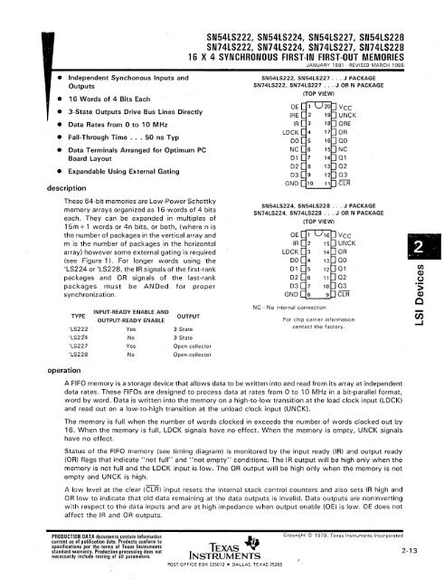
- Page 49 and 50: SN54LS222, SN54LS224, SN74LS222, SN
- Page 51 and 52: SN54LS227, SN54LS228, SN74LS227, SN
- Page 53 and 54: ~SN54lS222, SN54lS224, SN54lS227, S
- Page 55 and 56: SN74S22516 x 5 ASYNCHRONOUS FIRST·
- Page 57 and 58: SN74S22516 x 5 ASYNCHRONOUS FIRST·
- Page 59 and 60: SN74S22516 x 5 ASYNCHRONOUS FIRST·
- Page 61 and 62: SN54ALS229A. SN74ALS229A16 x 5 ASYN
- Page 63 and 64: SN54ALS229A, SN74ALS229A16 x 5 ASYN
- Page 65 and 66: IrC/)cCD
- Page 67 and 68: SN54ALS232A, SN74ALS232A16 x 4 ASYN
- Page 69 and 70: SN54ALS232A, SN74ALS232A16 x 4 ASYN
- Page 71 and 72: SN54ALS233A, SN74ALS233A16 x 5 ASYN
- Page 73 and 74: SN54ALS233A, SN74ALS233A16 x 5 ASYN
- Page 75 and 76: SN54ALS233A,SN74ALS233A16 x 5 ASYNC
- Page 77 and 78: SN74AS2501·0F·16 DATA GENERATORS/
- Page 79 and 80: SN74AS2501·0F·16 DATA GENERATORS/
- Page 81 and 82: SN54ALS280, SN74ALS2809-BITPARITY G
- Page 83 and 84: SN54AS280, SN74AS2809·81T PARITY G
- Page 85 and 86: SN54ALS280, SN54AS280, SN74ALS280,
- Page 87 and 88: SN54AS286, SN74AS2869·BIT PARITY G
- Page 89 and 90: SN54AS286, SN74AS2869·BIT PARITY G
- Page 91 and 92: I2-58
- Page 93 and 94: SN54LS610 THRU SN54LS613, SN74LS610
- Page 95 and 96: SN54LS610 THRU SN54LS613, SN74LS610
- Page 97 and 98:
SN54LS610, SN54LS612, SN74LS610, SN
- Page 99 and 100:
SN54LS611, SN54LS613, SN74LS611, SN
- Page 101 and 102:
SN54LS610 THRU SN54LS613, SN74LS610
- Page 103 and 104:
SN54ALS616, SN54ALS617, SN74ALS616,
- Page 105 and 106:
SN54ALS616, SN54ALS617, SN74ALS616,
- Page 107 and 108:
SN54ALS616, SN54ALS617, SN74ALS616,
- Page 109 and 110:
SN54ALS616, SN54ALS617, SN74ALS616,
- Page 111 and 112:
SN54ALS617, SN74ALS61716·81T PARAL
- Page 113 and 114:
SN54ALS616, SN54ALS617, SN74ALS616,
- Page 115 and 116:
SN54ALS632A, SN54ALS633 THRU SN54AL
- Page 117 and 118:
SN54ALS632A, SN54ALS633 THRU SN54AL
- Page 119 and 120:
SN54ALS632A, SN54ALS633 THRU SN54AL
- Page 121 and 122:
SN54ALS632A, SN54ALS633, SN74ALS632
- Page 123 and 124:
SN5'4ALS632A, SN54ALS633 THRU SN54A
- Page 125 and 126:
SN54ALS634. SN74ALS63432·81T PARAL
- Page 127 and 128:
SN54ALS635, SN74ALS63532·81T PARAL
- Page 129 and 130:
SN54ALS632A, SN54ALS633 THRU SN54AL
- Page 131 and 132:
SN54AS632, SN54AS634SN74AS632, SN74
- Page 133 and 134:
SN54AS632, SN54AS634SN74AS632, SN74
- Page 135 and 136:
SN54AS632, SN54AS634SN74AS632, SN74
- Page 137 and 138:
ERROR~ ,SN54AS632, SN74AS63232·81T
- Page 139 and 140:
SN54AS632, SN54AS634SN74AS632, SN74
- Page 141 and 142:
SN54AS634, SN74AS63432·BIT PARALLE
- Page 143 and 144:
IrC/)C(1)
- Page 145 and 146:
SN54ALS646 THRU SN54ALS649, SN54AS6
- Page 147 and 148:
SN54ALS646 THRU SN54ALS649, SN54AS6
- Page 149 and 150:
SN54ALS646, SN74ALS646OCTAL BUS TRA
- Page 151 and 152:
SN54ALS647, SN74ALS647OCTAL BUS TRA
- Page 153 and 154:
SN54ALS648, SN74ALS648OCTAL BUS TRA
- Page 155 and 156:
SN54ALS649, SN74ALS649OCTAL BUS TRA
- Page 157 and 158:
SN54AS646, SN54AS648, SN74AS646, SN
- Page 159 and 160:
SN54ALS651 THRU SN54ALS654, SN54AS6
- Page 161 and 162:
SN54ALS651 THRU SN54ALS654, SN54AS6
- Page 163 and 164:
SN54ALS651, SN54ALS652, SN74ALS651,
- Page 165 and 166:
SN54ALS653, SN54ALS654, SN74ALS653,
- Page 167 and 168:
SN54ALS654, SN74ALS654OCTAL BUS TRA
- Page 169 and 170:
SN54AS651, SN54AS654, SN74AS651, SN
- Page 171 and 172:
SN54ALS666, SN54ALS667, SN74ALS666,
- Page 173 and 174:
SN54ALS666, SN54ALS667, SN74ALS666,
- Page 175 and 176:
SN54ALS666, SN54ALS667, SN74ALS666,
- Page 177 and 178:
II2-144
- Page 179 and 180:
SN54AS821, SN74AS82110-BIT BUS INTE
- Page 181 and 182:
SN54AS821, SN54AS822, SN74AS821, SN
- Page 183 and 184:
IIIrenc(1)
- Page 185 and 186:
SN54AS823, SN54AS824, SN74AS823, SN
- Page 187 and 188:
SN54AS823, SN54AS824, SN74AS823, SN
- Page 189 and 190:
Irenc(1)
- Page 191 and 192:
SN54AS825. SN54AS826. SN74AS825. SN
- Page 193 and 194:
SN54AS825, SN54AS826, SN74AS825, SN
- Page 195 and 196:
II2-162
- Page 197 and 198:
SN54ALS841, SN54AS841, SN54ALS842,
- Page 199 and 200:
SN54ALS841, SN74ALS84110·BIT BUS I
- Page 201 and 202:
SN54ALS842, SN74ALS84210·BIT BUS I
- Page 203 and 204:
SN54AS841, SN54AS842SN74AS841, SN74
- Page 205 and 206:
f·rrncCD
- Page 207 and 208:
SN54ALS843, SN54AS843, SN54ALS844,
- Page 209 and 210:
SN54ALS843, SN54ALS844SN74ALS843, S
- Page 211 and 212:
SN54AS843. SN54AS844SN74AS843. SN74
- Page 213 and 214:
SN54ALS843, SN54AS843, SN54ALS844,
- Page 215 and 216:
SN54ALS845, SN54AS845, SN54ALS846,
- Page 217 and 218:
SN54ALS845, SN74ALS8458·BIT BUS IN
- Page 219 and 220:
SN54ALS846, SN74ALS8468·BIT BUS IN
- Page 221 and 222:
SN54AS845, SN54AS846SN74AS845, SN74
- Page 223 and 224:
IrencCD
- Page 225 and 226:
SN74AS850. SN74AS8511 OF 16 DATA SE
- Page 227 and 228:
SN74AS850, SN74AS8511 OF 16 DATA SE
- Page 229 and 230:
SN74AS8511 OF 16 DATA SELECTORS/MUL
- Page 231 and 232:
SN74AS850, SN74AS8511 OF 16 DATA SE
- Page 233 and 234:
SN74AS8501 OF 16 DATA SELECTORS/MUL
- Page 235 and 236:
SN54AS852, SN74AS8528·BIT UNIVERSA
- Page 237 and 238:
SN54AS852, SN74AS8528·BIT UNIVERSA
- Page 239 and 240:
SN54ASB52. SN74ASB52B·BIT UNIVERSA
- Page 241 and 242:
SN54AS856, SN74AS8568·BIT UNIVERSA
- Page 243 and 244:
SN54AS856, SN74AS8568-BIT UNIVERSAL
- Page 245 and 246:
IIIrencCD
- Page 247 and 248:
SN54AS867, SN54AS869, SN74AS867, SN
- Page 249 and 250:
SN54AS867, SN74AS867SYNCHRONOUS 8-B
- Page 251 and 252:
SN54AS867, SN54AS869, SN74AS867, SN
- Page 253 and 254:
SN54AS870, SN54AS871, SN74AS870, SN
- Page 255 and 256:
SN54AS870, SN54AS871, SN74AS870, SN
- Page 257 and 258:
SN54AS870, SN54AS871, SN74AS870, SN
- Page 259 and 260:
SN54AS877, SN74AS8778-BIT UNIVERSAL
- Page 261 and 262:
SN54AS877, SN74AS8778-BIT UNIVERSAL
- Page 263 and 264:
SN54AS877, SN74AS8778·BIT UNIVERSA
- Page 265 and 266:
SN54AS882A, SN74AS882A32·BIT LOOK
- Page 267 and 268:
~SN54AS882A, SN74AS882A32·81T LOOK
- Page 269 and 270:
SN54AS882A, SN74AS882A32·81T LOOK
- Page 271 and 272:
~SN54AS882A, SN74AS882A32·81T LOOK
- Page 273 and 274:
SN54AS885, SN74AS8858·BIT MAGNITUD
- Page 275 and 276:
SN54AS885, SN74AS8858·BIT MAGNITUD
- Page 277 and 278:
SN54AS885, SN74AS8858-BIT MAGNITUDE
- Page 279 and 280:
SN54AS887. SN74AS8878·BIT PROCESSO
- Page 281 and 282:
SN54AS887, SN74AS8878·BIT PROCESSO
- Page 283 and 284:
SN54AS887, SN74AS8878·BIT PROCESSO
- Page 285 and 286:
SN54AS887, SN74AS8878·BIT PROCESSO
- Page 287 and 288:
SN54AS887, SN74AS8878·BIT PROCESSO
- Page 289 and 290:
SN54AS887, SN74AS8878·BIT PROCESSO
- Page 291 and 292:
SN54AS887. SN74AS8878·BIT PROCESSO
- Page 293 and 294:
SN54AS887, SN74AS8878·BIT PROCESSO
- Page 295 and 296:
SN54AS887, SN74AS8878·BIT PROCESSO
- Page 297 and 298:
SN54AS887, SN74AS8878·BIT PROCESSO
- Page 299 and 300:
SN54AS887. SN74AS8878·BIT PROCESSO
- Page 301 and 302:
SN54ASBB7, SN74ASBB7B·BIT PROCESSO
- Page 303 and 304:
SN54AS887, SN74AS8878·BIT PROCESSO
- Page 305 and 306:
SN54AS887. SN74AS8878·BIT PROCESSO
- Page 307 and 308:
SN54AS887, SN74AS8878·BIT PROCESSO
- Page 309 and 310:
SN54AS887, SN74AS8878·BIT PROCESSO
- Page 311 and 312:
SN54AS887, SN74AS8878·BIT PROCESSO
- Page 313 and 314:
SN54ASQ87, SN74AS8878·BIT PROCESSO
- Page 315 and 316:
SN54AS887, SN74AS887B·BIT PROCESSO
- Page 317 and 318:
SN54AS887, SN74AS8878·BIT PROCESSO
- Page 319 and 320:
SN54AS887, SN74AS8878·BIT PROCESSO
- Page 321 and 322:
SN54ASBB7, SN74ASBB7B·BIT PROCESSO
- Page 323 and 324:
SN54ASBB7. SN74ASBB7B·BIT PROCESSO
- Page 325 and 326:
IIrC/)cCD
- Page 327 and 328:
~SN54AS888, SN74AS8888·BIT PROCESS
- Page 329 and 330:
SN54AS888, SN74AS88B8·BIT PROCESSO
- Page 331 and 332:
SN54AS888, SN74AS8888·BIT PROCESSO
- Page 333 and 334:
SN54AS888, SN74AS8888·BIT PROCESSO
- Page 335 and 336:
SN54ASBBB, SN74ASBBBB·BIT PROCESSO
- Page 337 and 338:
SN54AS888, SN74AS8888-BIT PROCESSOR
- Page 339 and 340:
SN54AS888, SN74AS8888·BIT PROCESSO
- Page 341 and 342:
NWo00SERIAL DATA INPUT (CRU)(FILLS
- Page 343 and 344:
SN54AS888, SN74AS8888·BIT PROCESSO
- Page 345 and 346:
lr-(J)C~=...Jz0a~I-~:I:~a:...Je:(
- Page 347 and 348:
SN54AS888, SN74AS8888·BIT PROCESSO
- Page 349 and 350:
SN54AS888, SN74AS8888·BIT PROCESSO
- Page 351 and 352:
SN54AS888, SN74AS8888·BIT PROCESSO
- Page 353 and 354:
SN54AS888, SN74AS8888·BIT PROCESSO
- Page 355 and 356:
SN54AS888. SN74AS8888·BIT PROCESSO
- Page 357 and 358:
SN54AS888, SN74AS8888·BIT PROCESSO
- Page 359 and 360:
SN54AS888, SN74AS8888·BIT PROCESSO
- Page 361 and 362:
SN54AS888, SN74AS8888·BIT PROCESSO
- Page 363 and 364:
SN54AS888, SN74AS8888·BIT PROCESSO
- Page 365 and 366:
SN54AS888, SN74AS8888-BIT PROCESSOR
- Page 367 and 368:
SN54AS888, SN74AS8888·BIT PROCESSO
- Page 369 and 370:
SN54AS888, SN74AS8888-BIT PROCESSOR
- Page 371 and 372:
SN54AS888, SN74AS8888-BIT PROCESSOR
- Page 373 and 374:
SN54AS888, SN74AS8888-BIT PROCESSOR
- Page 375 and 376:
SN54AS888, SN74AS8888-BIT PROCESSOR
- Page 377 and 378:
SN54AS890, SN74AS890MICROSEOUENCERS
- Page 379 and 380:
SN54AS890, SN74AS890MICROSEOUENCERS
- Page 381 and 382:
SN54AS890, SN74AS890MICROSEOUENCERS
- Page 383 and 384:
SN54AS890, SN74AS890MICROSEOUENCERS
- Page 385 and 386:
SN54AS890, SN74AS890MICROSEOUENCERS
- Page 387 and 388:
SN54AS890, SN74AS890MICROSEOUENCERS
- Page 389 and 390:
SN54AS890, SN74AS890MICROSEOUENCERS
- Page 391 and 392:
SN54AS890MICROSEOUENCERSSN54AS890 m
- Page 393 and 394:
SN74Asa90·1MICROSEOUENCERSSN74AS89
- Page 395 and 396:
SN54AS895, SN74AS8958·BIT MEMORY A
- Page 397 and 398:
SN54AS895, SN74AS8958·BIT MEMORY A
- Page 399 and 400:
SN54AS895, SN74AS8958·BIT MEMORY A
- Page 401 and 402:
SN54AS895, SN74AS8958-BIT MEMORY AD
- Page 403 and 404:
SN54AS895, SN74AS8958·BIT MEMORY A
- Page 405 and 406:
SN54AS895, SN74ASB~5B·BIT MEMORY A
- Page 407 and 408:
SN54AS895, SN74AS8958·BIT MEMORY A
- Page 409 and 410:
SN54AS895. SN74AS8958·BIT MEMORY A
- Page 411 and 412:
SN54AS895, SN74AS8958·BIT MEMORY A
- Page 413 and 414:
SN54AS895, SN74AS8958·BIT MEMORY A
- Page 415 and 416:
SN54AS895, SN74AS8958·BIT MEMORY A
- Page 417 and 418:
SN54AS895, SN74AS8958·BIT MEMORY A
- Page 419 and 420:
SN54AS895, SN74AS8958·BIT MEMORY A
- Page 421 and 422:
SN54AS095, SN74AS095O·BIT MEMORY A
- Page 423 and 424:
vSN54AS895, SN74AS8958·BIT MEMORY
- Page 425 and 426:
SN54AS895, SN74AS8958·BIT MEMORY A
- Page 427 and 428:
SN54AS895, SN74AS8958·BITMEMORY AD
- Page 429 and 430:
SN54AS895, SN74AS8958·BIT MEMORY A
- Page 431 and 432:
SN54AS895, SN74AS8958·BIT MEMORY A
- Page 433 and 434:
SN54AS895, SN74AS8958·BIT MEMORY A
- Page 435 and 436:
SN54AS895, SN74AS8958·BIT MEMORY A
- Page 437 and 438:
SN54AS895, SN74AS8958-BIT MEMORY AD
- Page 439 and 440:
SN54AS895, SN74AS8958·BIT MEMORY A
- Page 441 and 442:
SN54AS895, SN74AS8958·BIT MEMORY A
- Page 443 and 444:
SN54AS095, SN74AS095O·BIT MEMORY A
- Page 445 and 446:
SN54AS897A, SN74AS897A16·BIT PARAL
- Page 447 and 448:
SN54AS897A, SN74AS897A16·BIT PARAL
- Page 449 and 450:
SN54AS897A. SN74AS897A16·BIT PARAL
- Page 451 and 452:
SN54AS897A, SN74AS897A16·BIT PARAL
- Page 453 and 454:
SN54AS897A, SN74AS897A16·BIT PARAL
- Page 455 and 456:
SN54AS897A, SN74AS897A16·BIT PARAL
- Page 457 and 458:
SN54AS897A, SN74AS897A16·BIT PARAL
- Page 459 and 460:
SN54AS897A, SN74AS897A16-BIT PARALL
- Page 461 and 462:
SN54AS897A, SN74AS897A16·BIT PARAL
- Page 463 and 464:
SN54ALS963, SN74ALS963DUAL·RANK 8
- Page 465 and 466:
SN54ALS963, SN74ALS963DUAL·RANK 8
- Page 467 and 468:
SN54ALS964, SN74ALS964DUAL-RANK 8-B
- Page 469 and 470:
SN54ALS963, SN74ALS963DUAL·RANK 8
- Page 471 and 472:
SN54ALS963, SN54ALS964, SN74ALS963,
- Page 473 and 474:
SN54ALS963, SN54ALS964, SN74ALS963,
- Page 475 and 476:
SN74ALS990, SN74ALS9918·BIT D·TVP
- Page 477 and 478:
SN74ALS990, SN74ALS9918·BIT D·TVP
- Page 479 and 480:
SN74ALS990, SN74ALS9918-BIT D-TVPE
- Page 481 and 482:
2-448
- Page 483 and 484:
SN74ALS992, SN74ALS9939·BIT D·TVP
- Page 485 and 486:
SN74ALS992, SN74ALS9939·BIT D·TYP
- Page 487 and 488:
SN74ALS992, SN74ALS9939·BIT D·TVP
- Page 489 and 490:
lEIrencCD
- Page 491 and 492:
SN74ALS994, SN74ALS99510·BIT D·TV
- Page 493 and 494:
SN74ALS994, SN74ALS99510·BI1 D·TY
- Page 495 and 496:
SN74ALS994, SN74ALS99510·BIT D·TY
- Page 497 and 498:
IIrencCD
- Page 499 and 500:
SN74ALS9968·BIT D·TVPE EDGE·TRIG
- Page 501 and 502:
SN74ALS996H·BIT D·TYPE EDGE·TRIG
- Page 503 and 504:
SN74ALS996H·BIT D·TVPE EDGE·TRIG
- Page 505 and 506:
SN54AS 1181, SN74ASl181ARITHMETIC L
- Page 507 and 508:
SN54AS1181, SN74AS1181ARITHMETIC LO
- Page 509 and 510:
SN54ASl181, SN74ASl181ARITHMETIC LO
- Page 511 and 512:
SN54ASl181, SN74ASl181ARITHMETIC LO
- Page 513 and 514:
SN54AS1181, SN74AS1181ARITHMETIC LO
- Page 515 and 516:
SN54AS1181, SN74AS1181ARITHMETIC LO
- Page 517 and 518:
SN54ALS2967, SN74ALS2967, SN54ALS29
- Page 519 and 520:
SN54ALS2967, SN74ALS2967, SN54ALS29
- Page 521 and 522:
SN54ALS2967, SN74ALS2967, SN54ALS29
- Page 523 and 524:
SN54ALS2967, SN74ALS2967, SN54ALS29
- Page 525 and 526:
SN54ALS2967, SN74ALS2967, SN54ALS29
- Page 527 and 528:
SN54ALS2967, SN74ALS2967DYNAMIC MEM
- Page 529 and 530:
SN54ALS2967, SN74ALS2967, SN54ALS29
- Page 531 and 532:
SN54ALS2967, SN74ALS2967, SN54ALS29
- Page 533 and 534:
SN54ALS2967, SN74ALS2967, SN54ALS29
- Page 535 and 536:
SN54ALS2967, SN74ALS2967, SN54ALS29
- Page 537 and 538:
SN54ALS6301, SN74ALS6301, SN54ALS63
- Page 539 and 540:
SN54ALS6301, SN74ALS6301, SN54ALS63
- Page 541 and 542:
IIrC/)cCD
- Page 543 and 544:
SN74ALS8400EXPANDABLE ERROR CHECKER
- Page 545 and 546:
(3~Nen ....N~~z~(J)~-i~;o~~C:~~~;:1
- Page 547 and 548:
SN54AS8834, SN74AS883440·81T REGIS
- Page 549 and 550:
SN54AS8834, SN74AS883440·81T REGIS
- Page 551 and 552:
SN54AS883~ SN74AS883440·81T REGIST
- Page 553 and 554:
SN54AS8834, SN74AS883440·811 REGIS
- Page 555 and 556:
SN54AS8834, SN74AS883440·81T REGIS
- Page 557 and 558:
SN54AS8838, SN74AS883832·BIT BARRE
- Page 559 and 560:
SN54AS8838, SN74AS883832-BIT BARREL
- Page 561 and 562:
SN54AS8838, SN74AS883832·BIT BARRE
- Page 563 and 564:
SN54AS8838, SN74AS883832·BIT BARRE
- Page 565 and 566:
SN74AS883832·81T BARREL SHIFTERSel
- Page 567 and 568:
SN54ALS29818, SN54ALS29819SN74ALS29
- Page 569 and 570:
SN54ALS29818, SN54ALS29819SN74ALS29
- Page 571 and 572:
SN54ALS29819SN74ALS298198·BIT DIAG
- Page 573 and 574:
SN54ALS29818, SN54ALS29819SN74ALS29
- Page 575 and 576:
SN54ALS29818SN74ALS298188·BIT DIAG
- Page 577 and 578:
SN54ALS29818, SN54ALS29819SN74ALS29
- Page 579 and 580:
SN54ALS29821, SN74ALS2982110·BIT B
- Page 581 and 582:
SN54AS29821, SN54AS29822, SN74AS298
- Page 583 and 584:
SN54AS29821. SN54AS29822. SN74AS298
- Page 585 and 586:
SN54ALS29823, SN54ALS29824, SN74ALS
- Page 587 and 588:
SN54ALS29823. SN54ALS29824. SN74ALS
- Page 589 and 590:
SN54ALS29823, SN54ALS29824, SN74ALS
- Page 591 and 592:
encCD
- Page 593 and 594:
SN54ALS29825, SN54ALS29826SN74ALS29
- Page 595 and 596:
SN54ALS29825; SN54ALS29826SN74ALS29
- Page 597 and 598:
SN54ALS29825, SN54ALS29826SN74ALS29
- Page 599 and 600:
SN54ALS29827, SN54ALS29828SN74ALS29
- Page 601 and 602:
IItSN54Als29827, SN54ALS29S28SN74AL
- Page 603 and 604:
lEIrCJ)cCD
- Page 605 and 606:
SN54ALS29861, SN54ALS29862SN74ALS29
- Page 607 and 608:
SN54ALS29861, SN54ALS29862SN74ALS29
- Page 609 and 610:
SN54ALS29861, SN54ALS29862SN74Als29
- Page 611 and 612:
SN54ALS29863, SN54ALS29864SN74ALS29
- Page 613 and 614:
SN54ALS29863. SN54ALS29864SN74ALS29
- Page 615 and 616:
encCD
- Page 617 and 618:
THCT1 01 0·160M, THCT1 01 0·140E,
- Page 619 and 620:
THCT1 01 0-16oM, THCT1 01 0-140E, T
- Page 621 and 622:
THCT1010·160M. THCT1010·140E. THC
- Page 623 and 624:
THCT1010·160M, THCT1010·140E, THC
- Page 625 and 626:
IIrencCD
- Page 627 and 628:
THCT2000M,THCT2000EDIRECTION DISCRI
- Page 629 and 630:
C/)cCD
- Page 631 and 632:
THCT4502DYNAMIC RAM CONTROLLERdescr
- Page 633 and 634:
THCT4502 . .DYNAMIC RAM CONTROLLERp
- Page 635 and 636:
THCT4502DYNAMIC RAM CONTROLLER.reco
- Page 637 and 638:
THCT4502DYNAMIC RAM CONTROLLERswitc
- Page 639 and 640:
THCT4502DYNAMIC RAM CONTROLLERCLK1r
- Page 641 and 642:
THCT4502DYNAMIC RAM CONTROLLERCLKAL
- Page 643 and 644:
THCT4502DYNAMIC RAM CONTROLLERIre
- Page 645 and 646:
encCD
- Page 647 and 648:
THCT29520, THCT29521MULTILEVEL PIPE
- Page 649 and 650:
THCT29520, THCT29521MULTILEVEL PIPE
- Page 651 and 652:
encCD
- Page 653 and 654:
TMS2150CACHE ADDRESS COMPARATORfunc
- Page 655 and 656:
TMS2150CACHE ADDRESS COMPARATORelec
- Page 657 and 658:
TMS2150CACHE ADDRESS COMPARATORPARA
- Page 659 and 660:
IIrencCD
- Page 661 and 662:
TMS4500ADYNAMIC·RAM CONTROLLERBLOC
- Page 663 and 664:
TMS4500ADYNAMIC·RAM CONTROLLERSTRA
- Page 665 and 666:
TMS4500ADYNAMIC-RAM CONTROLLERtimin
- Page 667 and 668:
TMS4500ADYNAMIC·RAM CONTROLLERIr
- Page 669 and 670:
TMS4500ADYNAMIC·RAM CONTROLLEREIr
- Page 671 and 672:
TMS4500ADYNAMIC·RAM CONTROLLERtypi
- Page 673 and 674:
TMS4500ADYNAMIC·RAM CONTROLLERtypi
- Page 675 and 676:
EI2-642
- Page 677 and 678:
3-2
- Page 679 and 680:
IMPORTANT NOTICETexas Instruments r
- Page 681 and 682:
II»"C~.(")Q).....o·:::::s:JJCD"Co
- Page 683 and 684:
List of Illustrations (Continued)Fi
- Page 685 and 686:
Table 1. Typical Performance Charac
- Page 687 and 688:
. I J I-MET ~eN SILICONCOMPOSITIONS
- Page 689 and 690:
R314knR750nVee5knOUTPUT0304':"R52.8
- Page 691 and 692:
overlap of transistor Q5. The same
- Page 693 and 694:
VIL -Low·Level Input Voltage-V2.0
- Page 695 and 696:
DC Noise MarginsNoise margin is a v
- Page 697 and 698:
100605040;: 30E~20e".,c..c.~10a.~i5
- Page 699 and 700:
with gate 2 at a high-logic state.
- Page 701 and 702:
operate satisfactorily. However, if
- Page 703 and 704:
lEIl>'C"2-(i'Q)r+0'~:0CD'Co"""Ir+tJ
- Page 705 and 706:
2. Decouple the supply voltage of l
- Page 707 and 708:
VOUT5V5VICC 20mA 50mAVec 0.2V 0.2Vg
- Page 709 and 710:
parts of the chassis and ground bus
- Page 711 and 712:
Printed Circuit Card ConductorsSign
- Page 713 and 714:
'ASOOvee = 5.0 VTA = 25°e..... ...
- Page 715 and 716:
6040'ALSOOAVee = 5.0 VTA = 25°eI D
- Page 717 and 718:
ovovTRANSITION (1 -+ 0)Figure 59. O
- Page 719 and 720:
3-44
- Page 721 and 722:
Table A-I is normally used (in comb
- Page 723 and 724:
IOHIO(ofl)lOSICCHICCLlligh-Ievel ou
- Page 725 and 726:
3-50
- Page 727 and 728:
IMPORTANT NOTICETexas Instruments (
- Page 729 and 730:
ceramic packages - side-braze (JD s
- Page 731 and 732:
efore SO and SI goes low. Again, th
- Page 733 and 734:
'LS646'ALS632ASERIESMEMORY3S-BIT WI
- Page 735 and 736:
TMS9900ADDRESSBUSMEMORYMAPPERREGIST
- Page 737 and 738:
Table III. Modes of OperationMAPPER
- Page 739 and 740:
A12· / ..MAO-MA3'41/6 'LS04~D1'01i
- Page 741 and 742:
TIMINGThe subject of how the mapper
- Page 743 and 744:
IMPORTANT NOTICETexas Instruments (
- Page 745 and 746:
Section 6Floating-Point System Desi
- Page 747 and 748:
3-72
- Page 749 and 750:
3-74
- Page 751 and 752:
D-5TIBPAL16L8-15DRBINTRBOEVOERAOESN
- Page 753 and 754:
Program 2-1. Logic Equations Used t
- Page 755 and 756:
Program 2-2. Expanded Product Terms
- Page 757 and 758:
12345678Program 2-3. Simulation Res
- Page 759 and 760:
IIProgram 2-5. Logic Equations Used
- Page 761 and 762:
Program 2-6. Expanded Product Terms
- Page 763 and 764:
12345678910111213Program 2-7. Simul
- Page 765 and 766:
Program 2-7. Simulation Results for
- Page 767 and 768:
Program 2-8. JEDEC Printout for Emu
- Page 769 and 770:
»Benchmark I: Comparison of Am2903
- Page 771 and 772:
Table 3-7. 'AS888-l/'AS890-1 Timing
- Page 773 and 774:
->MICROPROGRAM'AS888'AS888MEMORY (L
- Page 775 and 776:
Cf-'os~JodaMuo!~e:l!ldd"MICROPROGRA
- Page 777 and 778:
14MICROPROGRAMMEMORY.--____-:.;M.:.
- Page 779 and 780:
A ZERO signal is generated when the
- Page 781 and 782:
Table 4-2. Functional Listing of Fe
- Page 783 and 784:
Table 4-7. Assembler Code of Multip
- Page 785 and 786:
and provide control to choose betwe
- Page 787 and 788:
lEIl>'0'2..crDo)r+o·;:,:0CD'0o"""I
- Page 789 and 790:
C:J.p.SlJodaM UO!lR:l!ldd" IIRST)
- Page 791 and 792:
each of the nine possible time dela
- Page 793 and 794:
II»"'C"2-DA/DB-Z (46)50 nsDA/DB-+N
- Page 795 and 796:
CARRYUSED
- Page 797 and 798:
EI148 '100 '***********************
- Page 799 and 800:
53A$AOOOO. 01. 02.02.02.03.04.04.04
- Page 801 and 802:
STEP 2: CHOOSE AN ALGORITHM FOR Sin
- Page 803 and 804:
6B) Compute sin(x) == En=OR4 RO * R
- Page 805 and 806:
As before, the steps of this algori
- Page 807 and 808:
By slightly reorganizing the sequen
- Page 809 and 810:
STEP 9: DEFINE MICROINSTRUCTION FIE
- Page 811 and 812:
Table 6.1. Floating Point Sin (x) M
- Page 813 and 814:
Table 6.1. Floating Point Sin(x) Mi
- Page 815 and 816:
IMPORTANT NOTICETexas Instruments (
- Page 817 and 818:
Control, data and address buses sha
- Page 819 and 820:
Cf+:+:-s~JodaH UO!~e:>!ldd" .•1
- Page 821 and 822:
Addressing of the register files, b
- Page 823 and 824:
MICROCODEFIELDTable 4-1. Microcode
- Page 825 and 826:
~U1os~JOdau uone:>!lddv I.Table 4-4
- Page 827 and 828:
Table 4-6. Functional Listing of Mu
- Page 829 and 830:
emoved. Likewise, changing the opco
- Page 831 and 832:
Table 4-9. Critical Delay Path Anal
- Page 833 and 834:
5.1 Choose a Floating-Point Number
- Page 835 and 836:
5.4 Substitute Registers for Variab
- Page 837 and 838:
FSIN: SUBROUTINE; A) Reduce angle r
- Page 839 and 840:
9) Clear the implicit bit in SF3.SF
- Page 841 and 842:
3) Unpack A2 to get SF2 and A2RB =
- Page 843 and 844:
Cfen(Xls:uodaM uOrJ.eO!lddvSYSTEM I
- Page 845 and 846:
Cf--..Jos:uodaJ:l UOrl.eO!lddvTable
- Page 847 and 848:
Cf-..,JNs~JodaMuo!~eo!ldd"Table 5.1
- Page 849 and 850:
Cf-...I.J::.sJJodaH UO!Je:llldd'V.T
- Page 851 and 852:
'f-'-...J0)suodaH uo!~e;)!ldd'lf•
- Page 853 and 854:
III4-2
- Page 855 and 856:
MECHANICAL DATAD plastic "small out
- Page 857 and 858:
MECHANICAL DATAow plastic "small ou
- Page 859 and 860:
MECHANICAL DATAFK ceramic chip carr
- Page 861 and 862:
MECHANICAL DATA68-pin GB pin grid a
- Page 863 and 864:
MECHANICAL DATAJ ceramic dual-in-li
- Page 865 and 866:
MECHANICAL DATAJ ceramic dual-in-li
- Page 867 and 868:
MECHANICAL DATAN plastic dual-in-li
- Page 869 and 870:
MECHANICAL DATAN plastic dual-in-li
- Page 871 and 872:
II4-20
- Page 873 and 874:
TI WorldwideSales OfficesALABAMA: H
- Page 875 and 876:
PLACESTAMPHERETexas InstrumentsLite