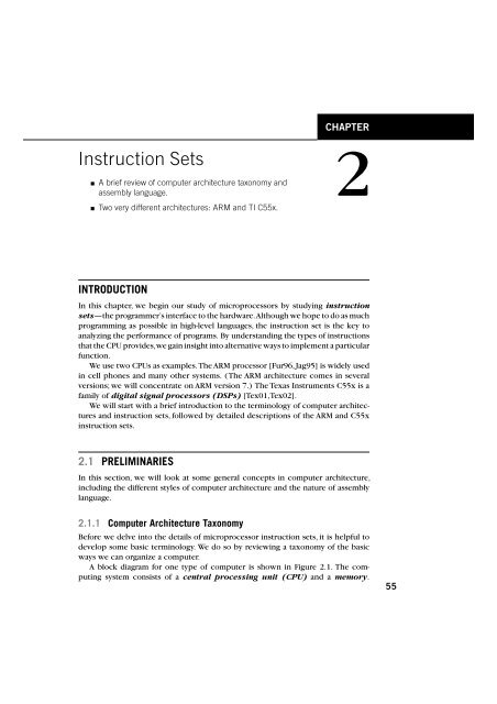
Instruction Sets
Instruction Sets
Instruction Sets

Create successful ePaper yourself
Turn your PDF publications into a flip-book with our unique Google optimized e-Paper software.
56 CHAPTER 2 <strong>Instruction</strong> <strong>Sets</strong>MemoryADD r5, r1, r3AddressDataCPUPCFIGURE 2.1A von Neumann architecture computer.Data memoryProgram memoryFIGURE 2.2A Harvard architecture.AddressDataAddress<strong>Instruction</strong>sCPUPCThe memory holds both data and instructions, and can be read or written whengiven an address. A computer whose memory holds both data and instructions isknown as a von Neumann machine.The CPU has several internal registers that store values used internally. One ofthose registers is the program counter (PC),which holds the address in memoryof an instruction.The CPU fetches the instruction from memory,decodes the instruction,and executes it. The program counter does not directly determine what themachine does next, but only indirectly by pointing to an instruction in memory. Bychanging only the instructions, we can change what the CPU does. It is this separationof the instruction memory from the CPU that distinguishes a stored-programcomputer from a general finite-state machine.An alternative to the von Neumann style of organizing computers is the Harvardarchitecture, which is nearly as old as the von Neumann architecture. As shownin Figure 2.2, a Harvard machine has separate memories for data and program.The program counter points to program memory, not data memory. As a result, it isharder to write self-modifying programs (programs that write data values, then usethose values as instructions) on Harvard machines.
2.1 Preliminaries 57Harvard architectures are widely used today for one very simple reason—theseparation of program and data memories provides higher performance for digitalsignal processing. Processing signals in real-time places great strains on the dataaccess system in two ways: First, large amounts of data flow through the CPU; andsecond,that data must be processed at precise intervals,not just when the CPU getsaround to it. Data sets that arrive continuously and periodically are called streamingdata. Having two memories with separate ports provides higher memory bandwidth;notmaking data and memory compete for the same port also makes it easierto move the data at the proper times. DSPs constitute a large fraction of all microprocessorssold today,and most of them are Harvard architectures.A single exampleshows the importance of DSP: Most of the telephone calls in the world go throughat least two DSPs, one at each end of the phone call.Another axis along which we can organize computer architectures relates totheir instructions and how they are executed. Many early computer architectureswere what is known today as complex instruction set computers (CISC).These machines provided a variety of instructions that may perform very complextasks, such as string searching; they also generally used a number of differentinstruction formats of varying lengths. One of the advances in the development ofhigh-performance microprocessors was the concept of reduced instruction setcomputers (RISC).These computers tended to provide somewhat fewer and simplerinstructions.The instructions were also chosen so that they could be efficientlyexecuted in pipelined processors. Early RISC designs substantially outperformedCISC designs of the period.As it turns out,we can use RISC techniques to efficientlyexecute at least a common subset of CISC instruction sets, so the performance gapbetween RISC-like and CISC-like instruction sets has narrowed somewhat.Beyond the basic RISC/CISC characterization,we can classify computers by severalcharacteristics of their instruction sets. The instruction set of the computerdefines the interface between software modules and the underlying hardware;the instructions define what the hardware will do under certain circumstances.<strong>Instruction</strong>s can have a variety of characteristics, including:■Fixed versus variable length.■ Addressing modes.■Numbers of operands.■ Types of operations supported.The set of registers available for use by programs is called the programmingmodel,also known as the programmer model. (The CPU has many other registersthat are used for internal operations and are unavailable to programmers.)There may be several different implementations of an architecture. In fact, thearchitecture definition serves to define those characteristics that must be true ofall implementations and what may vary from implementation to implementation.Different CPUs may offer different clock speeds, different cache configurations,
58 CHAPTER 2 <strong>Instruction</strong> <strong>Sets</strong>changes to the bus or interrupt lines, and many other changes that can make onemodel of CPU more attractive than another for any given application.2.1.2 Assembly LanguageFigure 2.3 shows a fragment ofARM assembly code to remind us of the basic featuresof assembly languages. Assembly languages usually share the same basic features:■■■One instruction appears per line.Labels, which give names to memory locations, start in the first column.<strong>Instruction</strong>s must start in the second column or after to distinguish them fromlabels.■ Comments run from some designated comment character (; in the case ofARM) to the end of the line.Assembly language follows this relatively structured form to make it easyfor the assembler to parse the program and to consider most aspects of theprogram line by line. (It should be remembered that early assemblers were writtenin assembly language to fit in a very small amount of memory. Those earlyrestrictions have carried into modern assembly languages by tradition.) Figure 2.4shows the format of an ARM data processing instruction such as an ADD. For theinstructionADDGT r0,r3,#5the cond field would be set according to the GT condition (1100), the opcode fieldwould be set to the binary code for the ADD instruction (0100), the first operandregister Rn would be set to 3 to represent r3, the destination register Rd would beset to 0 for r0, and the operand 2 field would be set to the immediate value of 5.Assemblers must also provide some pseudo-ops to help programmers createcomplete assembly language programs.An example of a pseudo-op is one that allowsdata values to be loaded into memory locations.These allow constants,for example,to be set into memory. An example of a memory allocation pseudo-op for ARM isshown in Figure 2.5. The ARM % pseudo-op allocates a block of memory of the sizespecified by the operand and initializes those locations to zero.label1ADR r4,cLDR r0,[r4]ADR r4,dLDR r1,[r4]SUB r0,r0,r1; a comment; another commentFIGURE 2.3An example of ARM assembly language.
2.2 ARM Processor 5931 27 25 24 20 19 15 11 0cond00 X opcode S Rn Rd Format determined by X bitX 5 1 (represents operand 2):11 7 0#rot 8-bit immediateX 5 0 format:11 6 4 3 0#shift Sh 0 Rm11 7 6 4 3 0Rs0Sh1RmFIGURE 2.4Format of ARM data processing instructions.FIGURE 2.5Pseudo-ops for allocating memory.BIGBLOCK % 102.2 ARM PROCESSORIn this section, we concentrate on the ARM processor. ARM is actually a familyof RISC architectures that have been developed over many years. ARM does notmanufacture its own VLSI devices; rather, it licenses its architecture to companieswho either manufacture the CPU itself or integrate the ARM processor into a largersystem.The textual description of instructions, as opposed to their binary representation,is called an assembly language. ARM instructions are written one perline, starting after the first column. Comments begin with a semicolon and continueto the end of the line. A label, which gives a name to a memory location,comes at the beginning of the line, starting in the first column. Here is anexample:labelLDR r0,[r8]; a commentADD r4,r0,r1
60 CHAPTER 2 <strong>Instruction</strong> <strong>Sets</strong>2.2.1 Processor and Memory OrganizationDifferent versions of theARM architecture are identified by different numbers. ARM7is a von Neumann architecture machine, while ARM9 uses a Harvard architecture.However, this difference is invisible to the assembly language programmer, exceptfor possible performance differences.The ARM architecture supports two basic types of data:■ The standard ARM word is 32 bits long.■ The word may be divided into four 8-bit bytes.ARM7 allows addresses up to 32 bits long.An address refers to a byte,not a word.Therefore, the word 0 in the ARM address space is at location 0, the word 1 is at 4,the word 2 is at 8,and so on. (As a result,the PC is incremented by 4 in the absenceof a branch.) The ARM processor can be configured at power-up to address thebytes in a word in either little-endian mode (with the lowest-order byte residingin the low-order bits of the word) or big-endian mode (the lowest-order bytestored in the highest bits of the word),as illustrated in Figure 2.6 [Coh81]. Generalpurposecomputers have sophisticated instruction sets. Some of this sophisticationis required simply to provide the functionality of a general computer, while otheraspects of instruction sets may be provided to increase performance, reduce codesize, or otherwise improve program characteristics. In this section, we concentrateon the functionality of theARM instruction set and will defer performance and otheraspects of the CPU to Section 5.6.Bit 31 Bit 0Word 4Byte 3 Byte 2 Byte 1 Byte 0Word 0Little-endianBit 31 Bit 0Word 4Byte 0 Byte 1 Byte 2 Byte 3Word 0FIGURE 2.6Byte organizations within an ARM word.Big-endian
2.2 ARM Processor 612.2.2 Data OperationsArithmetic and logical operations in C are performed in variables. Variables areimplemented as memory locations. Therefore, to be able to write instructions toperform C expressions and assignments, we must consider both arithmetic andlogical instructions as well as instructions for reading and writing memory.Figure 2.7 shows a sample fragment of C code with data declarations and severalassignment statements. The variables a, b, c, x, y, and z all become data locationsin memory. In most cases data are kept relatively separate from instructions in theprogram’s memory image.In the ARM processor, arithmetic and logical operations cannot be performeddirectly on memory locations. While some processors allow such operationsto directly reference main memory, ARM is a load-store architecture—dataoperands must first be loaded into the CPU and then stored back to main memoryto save the results. Figure 2.8 shows the registers in the basic ARM programmingmodel. ARM has 16 general-purpose registers, r0 through r15. Except for r15, theyare identical—any operation that can be done on one of them can be done on theother one also. The r15 register has the same capabilities as the other registers, butit is also used as the program counter.The program counter should of course not beoverwritten for use in data operations. However, giving the PC the properties of ageneral-purpose register allows the program counter value to be used as an operandin computations, which can make certain programming tasks easier.The other important basic register in the programming model is the currentprogram status register (CPSR). This register is set automatically duringevery arithmetic, logical, or shifting operation. The top four bits of the CPSRhold the following useful information about the results of that arithmetic/logicaloperation:■ The negative (N) bit is set when the result is negative in two’s-complementarithmetic.■ The zero (Z) bit is set when every bit of the result is zero.■ The carry (C) bit is set when there is a carry out of the operation.■ The overflow (V) bit is set when an arithmetic operation results in an overflow.FIGURE 2.7A C fragment with data operations.int a, b, c, x, y, z;x (a b) c;y a*(b c);z (a
2.2 ARM Processor 63The basic form of a data instruction is simple:ADD r0,r1,r2This instruction sets register r0 to the sum of the values stored in r1 and r2.In addition to specifying registers as sources for operands, instructions may alsoprovide immediate operands, which encode a constant value directly in theinstruction. For example,ADD r0,r1,#2sets r0 to r1 2.The major data operations are summarized in Figure 2.9. The arithmetic operationsperform addition and subtraction; the with-carry versions include the currentvalue of the carry bit in the computation. RSB performs a subtraction with the orderof the two operands reversed,so that RSB r0,r1,r2 sets r0 to be r2 r1.The bit-wiselogical operations perform logical AND, OR, and XOR operations (the exclusive oris called EOR). The BIC instruction stands for bit clear: BIC r0, r1, r2 sets r0 to r1and not r2. This instruction uses the second source operand as a mask:Where a bitin the mask is 1, the corresponding bit in the first source operand is cleared. TheMUL instruction multiplies two values,but with some restrictions:No operand maybe an immediate,and the two source operands must be different registers.The MLAinstruction performs a multiply-accumulate operation, particularly useful in matrixoperations and signal processing. The instructionMLA r0,r1,r2,r3sets r0 to the value r1 r2 r3.The shift operations are not separate instructions—rather, shifts can be appliedto arithmetic and logical instructions. The shift modifier is always applied to thesecond source operand. A left shift moves bits up toward the most-significant bits,while a right shift moves bits down to the least-significant bit in the word. The LSLand LSR modifiers perform left and right logical shifts, filling the least-significantbits of the operand with zeroes.The arithmetic shift left is equivalent to an LSL,butthe ASR copies the sign bit—if the sign is 0, a 0 is copied, while if the sign is 1, a1 is copied. The rotate modifiers always rotate right, moving the bits that fall offthe least-significant bit up to the most-significant bit in the word.The RRX modifierperforms a 33-bit rotate, with the CPSR’s C bit being inserted above the sign bit ofthe word; this allows the carry bit to be included in the rotation.The instructions in Figure 2.10 are comparison operations—they do not modifygeneral-purpose registers but only set the values of the NZCV bits of the CPSR register.The compare instruction CMP r0, r1 computes r0 – r1, sets the status bits, andthrows away the result of the subtraction. CMN uses an addition to set the status bits.TST performs a bit-wise AND on the operands, while TEQ performs an exclusive-or.Figure 2.11 summarizes the ARM move instructions. The instruction MOV r0, r1sets the value of r0 to the current value of r1. The MVN instruction complementsthe operand bits (one’s complement) during the move.
64 CHAPTER 2 <strong>Instruction</strong> <strong>Sets</strong>ADDADCSUBSBCRSBRSCMULMLAAddAdd with carrySubtractSubtract with carryReverse subtractReverse subtract with carryMultiplyMultiply and accumulateArithmeticANDORREORBICBit-wise andBit-wise orBit-wise exclusive-orBit clearLogicalLSLLSRASLASRRORRRXLogical shift left (zero fill)Logical shift right (zero fill)Arithmetic shift leftArithmetic shift rightRotate rightRotate right extended with CFIGURE 2.9ARM data instructions.Shift/rotateValues are transferred between registers and memory using the load-store instructionssummarized in Figure 2.12. LDRB and STRB load and store bytes rather thanwhole words,while LDRH and SDRH operate on half-words and LDRSH extends thesign bit on loading. An ARM address may be 32 bits long. The ARM load and storeinstructions do not directly refer to main memory addresses, since a 32-bit addresswould not fit into an instruction that included an opcode and operands. Instead,theARM uses register-indirect addressing. In register-indirect addressing,the value
2.2 ARM Processor 65CMPCMNTSTTEQCompareNegated compareBit-wise testBit-wise negated testFIGURE 2.10ARM comparison instructions.MOVMVNMoveMove negatedFIGURE 2.11ARM move instructions.LDRSTRLDRHSTRHLDRSHLDRBSTRBADRLoadStoreLoad half-wordStore half-wordLoad half-word signedLoad byteStore byteSet register to addressFIGURE 2.12ARM load-store instructions and pseudo-operations.stored in the register is used as the address to be fetched from memory; the resultof that fetch is the desired operand value. Thus, as illustrated in Figure 2.13, if weset r1 0 100, the instructionLDR r0,[r1]sets r0 to the value of memory location 0x100. Similarly, STR r0,[r1] would storethe contents of r0 in the memory location whose address is given in r1. There areseveral possible variations:LDR r0,[r1, – r2]
66 CHAPTER 2 <strong>Instruction</strong> <strong>Sets</strong>AddressData0 3 100r1031000 3 50 3 5r0CPUMemory<strong>Instruction</strong>: LDR r0,[r1]FIGURE 2.13Register-indirect addressing in the ARM.0 3 201 r150 3 201SUB r1, r15, #&101Distance 5 0 3 1010 3 100 FOO0 3 5MemoryFIGURE 2.14Computing an absolute address using the PC.loads r0 from the address given by r1 r2, whileLDR r0,[r1, #4]loads r0 from the address r1 4.This begs the question of how we get an address into a register—we need to beable to set a register to an arbitrary 32-bit value. In the ARM,the standard way to seta register to an address is by performing arithmetic on the program counter, whichis stored in r15. By adding or subtracting to the PC a constant equal to the distancebetween the current instruction (i.e.,the instruction that is computing the address)and the desired location,we can generate the desired address without performing aload. The ARM programming system provides an ADR pseudo-operation to simplify
2.2 ARM Processor 67this step. Thus, as shown in Figure 2.14, if we give location 0x100 the name FOO,we can use the pseudo-operationADR r1,FOOto perform the same function of loading r1 with the address 0x100.Example 2.2 illustrates how to implement C assignments in ARM instruction.Example 2.2C assignments in ARM instructionsWe will use the assignments of Figure 2.7. The semicolon (;) begins a comment after aninstruction, which continues to the end of that line. The statementx (a b) c;can be implemented by using r0 for a, r1forb, r2forc, and r3 for x. We also need registersfor indirect addressing. In this case, we will reuse the same indirect addressing register, r4,for each variable load. The code must load the values of a, b, and c into these registers beforeperforming the arithmetic, and it must store the value of x back to memory when it is done.This code performs the following necessary steps:ADR r4,a ; get address for aLDR r0,[r4] ; get value of aADR r4,b ; get address for b, reusing r4LDR r1,[r4] ; load value of bADD r3,r0,r1 ; set intermediate result for x to a + bADR r4,c ; get address for cLDR r2,[r4] ; get value of cSUB r3,r3,r2 ; complete computation of xADR r4,x ; get address for xSTR r3,[r4] ; store x at proper locationThe operationy a ∗ (b c);can be coded similarly, but in this case we will reuse more registers by using r0 for both a andb,r1forc, and r2 for y . Once again, we will use r4 to store addresses for indirect addressing.The resulting code isADR r4,b ; get address for bLDR r0,[r4] ; get value of bADR r4,c ; get address for cLDR r1,[r4] ; get value of cADD r2,r0,r1 ; compute partial result of yADR r4,a ; get address for a
68 CHAPTER 2 <strong>Instruction</strong> <strong>Sets</strong>LDR r0,[r4] ; get value of aMUL r2,r2,r0 ; compute final value of yADR r4,y ; get address for ySTR r2,[r4] ; store value of y at proper locationThe C statementz (a 2) | (b & 15);can be coded using r0 for a and z, r1forb, and r4 for addresses as follows:ADR r4,aLDR r0,[r4]MOV r0,r0,LSL 2ADR r4,bLDR r1,[r4]AND r1,r1,#15ORR r1,r0,r1ADR r4,zSTR r1,[r4]; get address for a; get value of a; perform shift; get address for b; get value of b; perform logical AND; compute final value of z; get address for z; store value of zWe have already seen three addressing modes: register, immediate, and indirect.The ARM also supports several forms of base-plus-offset addressing, which isrelated to indirect addressing. But rather than using a register value directly asan address, the register value is added to another value to form the address. Forinstance,LDR r0,[r1,#16]loads r0 with the value stored at location r1 16. Here,r1 is referred to as the baseand the immediate value the offset. When the offset is an immediate, it may haveany value up to 4,096;another register may also be used as the offset.This addressingmode has two other variations:auto-indexing and post-indexing. Auto-indexingupdates the base register, such thatLDR r0,[r1,#16]!first adds 16 to the value of r1, and then uses that new value as the address. The! operator causes the base register to be updated with the computed address sothat it can be used again later. Our examples of base-plus-offset and auto-indexinginstructions will fetch from the same memory location, but auto-indexing will alsomodify the value of the base register r1. Post-indexing does not perform the offsetcalculation until after the fetch has been performed. Consequently,LDR r0,[r1],#16will load r0 with the value stored at the memory location whose address is given byr1, and then add 16 to r1 and set r1 to the new value. In this case, the post-indexed
2.2 ARM Processor 69mode fetches a different value than the other two examples, but ends up with thesame final value for r1 as does auto-indexing.We have used the ADR pseudo-op to load addresses into registers to access variablesbecause this leads to simple, easy-to-read code (at least by assembly languagestandards). Compilers tend to use other techniques to generate addresses, becausethey must deal with global variables and automatic variables.2.2.3 Flow of ControlThe B (branch) instruction is the basic mechanism in ARM for changing the flow ofcontrol.The address that is the destination of the branch is often called the branchtarget. Branches are PC-relative—the branch specifies the offset from the currentPC value to the branch target. The offset is in words, but because the ARM is byteaddressable,the offset is multiplied by four (shifted left two bits, actually) to form abyte address. Thus, the instructionB #100will add 400 to the current PC value.We often wish to branch conditionally,based on the result of a given computation.The if statement is a common example. The ARM allows any instruction, includingbranches, to be executed conditionally. This allows branches to be conditional, aswell as data operations. Figure 2.15 summarizes the condition codes.EQ Equals zero Z 5 1NE Not equal to zero Z 5 0CS Carry set C 5 1CC Carry clear C 5 0MI Minus N 5 1PL Nonnegative (plus) N 5 0VS Overflow V 51VC No overflow V 5 0HI Unsigned higher C 5 1 and Z 5 0LS Unsigned lower or same C 5 0 or Z 5 1GE Signed greater than or equal N 5 VLT Signed less than N VGT Signed greater than Z 5 0 and N 5 VLE Signed less than or equal Z 5 1 or N VFIGURE 2.15Condition codes in ARM.
70 CHAPTER 2 <strong>Instruction</strong> <strong>Sets</strong>Example 2.3 shows how to implement an if statement.Example 2.3Implementing an if statement in ARMWe will use the following if statement as an example:if (a < b) {x = 5;y = c + d;}else x = c – d;The implementation uses two blocks of code, one for the true case and another for the falsecase. A branch may either fall through to the true case or branch to the false case:; compute and test the conditionADR r4,a ; get address for aLDR r0,[r4] ; get value of aADR r4,b ; get address for bLDR r1,[r4] ; get value of bCMP r0, r1 ; compare a < bBGE fblock ; if a >= b, take branch; the true block followsMOV r0,#5 ; generate value for xADR r4,x ; get address for xSTR r0,[r4] ; store value of xADR r4,c ; get address for cLDR r0,[r4] ; get value of cADR r4,d ; get address for dLDR r1,[r4] ; get value of dADD r0,r0,r1 ; compute c + dADR r4,y ; get address for ySTR r0,[r4] ; store value of yB after ; branch around the false block; the false block followsfblock ADR r4,c ; get address for cLDR r0,[r4] ; get value of cADR r4,d ; get address for dLDR r1,[r4] ; get value of dSUB r0,r0,r1 ; compute c – dADR r4,x ; get address for xSTR r0,[r4] ; store value of xafter ... ; code after the if statement
2.2 ARM Processor 71Example 2.4 illustrates an interesting way to implement multiway conditions.Example 2.4Implementing the C switch statement in ARMThe switch statement in C takes the following form:switch (test) {case 0: ... break;case 1: ... break;...}The above statement could be coded like an if statement by first testing test A, then test B,and so forth. However, it can be more efficiently implemented by using base-plus-offsetaddressing and building what is known as a branch table:ADR r2,test ; get address for testLDR r0,[r2] ; load value for testADR r1,switchtab ; load address for switch tableLDR r15,[r1,r0,LSL #2]switchtab DCD case0DCD case1...case0 ... ; code for case 0...case1 ... ; code for case 1...This implementation uses the value of test as an offset into a table, where the table holds theaddresses for the blocks of code that implement the various cases. The heart of this code isthe LDR instruction, which packs a lot of functionality into a single instruction:■ It shifts the value of r0 left two bits to turn the offset into a word address.■ It uses base-plus-offset addressing to add the left-shifted value of test (held in r0) to theaddress of the base of the table held in r1.■ It sets the PC (r15) to the new address computed by the instruction.Each case is implemented by a block of code that is located elsewhere in memory. Thebranch table begins at the location named switchtab. The DCD statement is a way of loadinga 32-bit address into memory at that point, so the branch table holds the addresses of thestarting points of the blocks that correspond to the cases.The loop is a very common C statement, particularly in signal processing code.Loops can be naturally implemented using conditional branches. Because loops
72 CHAPTER 2 <strong>Instruction</strong> <strong>Sets</strong>often operate on values stored in arrays,loops are also a good illustration of anotheruse of the base-plus-offset addressing mode. A simple but common use of a loopis in the FIR filter, which is explained in Application Example 2.1; the loop-basedimplementation of the FIR filter is described in Example 2.5.Application Example 2.1FIR filtersA finite impulse response (FIR) filter is a commonly used method for processing signals; wemake use of it in Section 5.11. The FIR filter is a simple sum of products:∑c r x i (2.1)1≤i≤nIn use as a filter, the x i s are assumed to be samples of data taken periodically, while the c i sare coefficients. This computation is usually drawn like this:fc c 14c 2 c3x 1 x 2x 3 x 4. . .This representation assumes that the samples are coming in periodically and that the FIRfilter output is computed once every time a new sample comes in. The boxes represent delayelements that store the recent samples to provide the x i s. The delayed samples are individuallymultiplied by the c i s and then summed to provide the filter output.Example 2.5An FIR filter for the ARMThe C code for the FIR filter of Application Example 2.1 follows:for (i = 0, f = 0; i < N; i++)f = f + c[i] * x[i];We can address the arrays c and x using base-plus-offset addressing: We will load one registerwith the address of the zeroth element of each array and use the register holding i as the offset.The C language [Ker88] defines a for loop as equivalent to a while loop with properinitialization and termination. Using that rule, the for loop can be rewritten asi = 0;f = 0;
2.2 ARM Processor 73while (i < N) {f = f + c[i]*x[i];i++;}Here is the code for the loop:; loop initiation codeMOV r0,#0 ; use r0 for i, set to 0MOV r8,#0 ; use a separate index for arraysADR r2,N ; get address for NLDR r1,[r2] ; get value of N for loop termination testMOV r2,#0 ; use r2 for f, set to 0ADR r3,c ; load r3 with address of base of c arrayADR r5,x ; load r5 with address of base of x array; loop bodyloop LDR r4,[r3,r8] ; get value of c[i]LDR r6,[r5,r8] ; get value of x[i]MUL r4,r4,r6 ; compute c[i]*x[i]ADD r2,r2,r4 ; add into running sum f; update loop counter and array indexADD r8,r8,#4 ; add one word offset to array indexADD r0,r0,#1 ; add 1 to i; test for exitCMP r0,r1BLT loop ; if i < N, continue looploopend...We have to be careful about numerical accuracy in this type of code, whether it is written in Cor assembly language. The result of a 32-bit 32-bit multiplication is a 64-bit result. The ARMMUL instruction leaves the lower 32 bits of the result in the destination register. So long asthe result fits within 32 bits, this is the desired action. If the input values are such that valuescan sometimes exceed 32 bits, then we must redesign the code to compute higher-resolutionvalues.The other important class of C statement to consider is the function. A C functionreturns a value (unless its return type is void); subroutine or procedure arethe common names for such a construct when it does not return a value. Considerthis simple use of a function in C:x = a + b;foo(x);y = c - d;A function returns to the code immediately after the function call, in this case theassignment to y. A simple branch is insufficient because we would not know where
74 CHAPTER 2 <strong>Instruction</strong> <strong>Sets</strong>to return. To properly return, we must save the PC value when the procedure/function is called and, when the procedure is finished, set the PC to the address ofthe instruction just after the call to the procedure. (You don’t want to endlesslyexecute the procedure,after all.) The branch-and-link instruction is used in theARMfor procedure calls. For instance,BL foowill perform a branch and link to the code starting at location foo (using PC-relativeaddressing,of course).The branch and link is much like a branch,except that beforebranching it stores the current PC value in r14. Thus, to return from a procedure,you simply move the value of r14 to r15:MOV r15,r14You should not, of course, overwrite the PC value stored in r14 during theprocedure.But this mechanism only lets us call procedures one level deep. If, for example,we call a C function within another C function, the second function call willoverwrite r14,destroying the return address for the first function call.The standardprocedure for allowing nested procedure calls (including recursive procedure calls)is to build a stack,as illustrated in Figure 2.16.The C code shows a series of functionsthat call other functions: f1( ) calls f2( ), which in turn calls f3( ). The right side ofvoid f1(int a) {f2(a);}void f2(int r) {f3(r,5);}f3f2Growthvoid f3(int x, int y) {g5 x 1 y;}main() {f1(xyz);}f1Function call stackFIGURE 2.16C codeNested function calls and stacks.
2.2 ARM Processor 75the figure shows the state of the procedure call stack during the execution off3( ). The stack contains one activation record for each active procedure. Whenf3( ) finishes, it can pop the top of the stack to get its return address, leaving thereturn address for f2( ) waiting at the top of the stack for its return.Most procedures need to pass parameters into the procedure and return valuesout of the procedure as well as remember their return address.We can also use the procedure call stack to pass parameters. The conventionsused to pass values into and out of procedures is known as procedure linkage.To pass parameters into a procedure, the values can be pushed onto the stackjust before the procedure call. Once the procedure returns, those values must bepopped off the stack by the caller, since they may hide a return address or otheruseful information on the stack. A procedure may also need to save register valuesfor registers it modifies. The registers can be pushed onto the stack upon entryto the procedure and popped off the stack, restoring the previous values, beforereturning.Example 2.6 illustrates the programming of a simple C function.Example 2.6Procedure calls in ARMWe use as an example one of the functions from Figure 2.16:void f1(int a) {f2(a);}The ARM C compiler’s convention is to use register r13 to point to the top of the stack. Weassume that the argument a has been passed into f1() on the stack and that we must pushthe argument for f2 (which happens to be the same value) onto the stack before calling f2().Here is some handwritten code for f1(), which includes a call to f2():f1 LDR r0,[r13] ; load value of a argument into r0 from stack; call f2()STR r14,[r13]! ; store f1's return address on the stackSTR r0,[r13!] ; store argument to f2 onto stackBL f2; branch and link to f2; return from f1()SUB r13,#4; pop f2's argument off the stackLDR r13!,r15 ; restore registers and returnWe use base-plus-offset addressing to load the value passed into f1() into a register for useby r1. To call f2(), we first push f1()’s return address, stored in r14 by the branch-and-linkinstruction executed to get into f1(), onto the stack. We then push f2()’s parameter onto thestack. In both cases, we use autoincrement addressing to both store onto the stack and adjustthe stack pointer. To return, we must first adjust the stack to get rid of f2()’s parameter that
76 CHAPTER 2 <strong>Instruction</strong> <strong>Sets</strong>hides f1()’s return address; we then use autoincrement addressing to pop f1()’s return addressoff the stack and into the PC (r15).We will discuss procedure linkage mechanisms for the ARM in more detail in Section 5.4.2.2.3 TI C55x DSPThe Texas Instruments C55x DSP is a family of digital signal processors designedfor relatively high performance signal processing. The family extends on previousgenerations of TI DSPs; the architecture is also defined to allow several differentimplementations that comply with the instruction set.The C55x,like many DSPs,is an accumulator architecture,meaning that manyarithmetic operations are of the form accumulator operand accumulator.Because one of the operands is the accumulator, it need not be specified in theinstruction. Accumulator-oriented instructions are also well-suited to the types ofoperations performed in digital signal processing, such as a 1 x 1 a 2 x 2 ....Ofcourse, the C55x has more than one register and not all instructions adhere to theaccumulator-oriented format. But we will see that arithmetic and logical operationstake a very different form in the C55x than they do in the ARM.C55x assembly language programs follow the typical format:MPY *AR0, *CDP+, AC0label: MOV #1, T0Assembler mnemonics are case-insensitive. <strong>Instruction</strong> mnemonics are formed bycombining a root with prefixes and/or suffixes. For example,theA prefix denotes anoperation performed in addressing mode while the 40 suffix denotes an arithmeticoperation performed in 40-bit resolution. We will discuss the prefixes and suffixesin more detail when we describe the instructions.The C55x also allows operations to be specified in an algebraic form:AC1 = AR0 * coef(*CDP)2.3.1 Processor and Memory OrganizationWe will use the term register to mean any type of register in the programmer modeland the term accumulator to mean a register used primarily in the accumulatorstyle.The C55x supports several data types:■ A word is 16 bits long.■ A longword is 32 bits long.■■<strong>Instruction</strong>s are byte-addressable.Some instructions operate on addressed bits in registers.
2.3 TI C55x DSP 77The C55x has a number of registers. Few to none of these registers are generalpurposeregisters like those of the ARM. Registers are generally used for specializedpurposes. Because the C55x registers are less regular, we will discuss them by howthey may be used rather than simply listing them.Most registers are memory-mapped—that is,the register has an address in thememory space. A memory-mapped register can be referred to in assembly languagein two different ways: either by referring to its mnemonic name or through itsaddress.The program counter is PC.The program counter extension register XPC extendsthe range of the program counter. The return address register RETA is used forsubroutines.The C55x has four 40-bit accumulators AC0,AC1,AC2, and AC3. The low-orderbits 0–15 are referred to as AC0L,AC1L,AC2L, and AC3L; the high-order bits 16–31are referred to as AC0H, AC1H, AC2H, and AC3H; and the guard bits 32–39 arereferred to as AC0G, AC1G, AC2G, and AC3G. (Guard bits are used in numericalalgorithms like signal processing to provide a larger dynamic range for intermediatecalculations.)The architecture provides six status registers. Three of the status registers,ST0 and ST1 and the processor mode status register PMST, are inherited fromthe C54x architecture. The C55x adds four registers ST0_55, ST1_55, ST2_55,and ST3_55. These registers provide arithmetic and bit manipulation flags, a datapage pointer and auxiliary register pointer, and processor mode bits, among otherfeatures.The stack pointer SP keeps track of the system stack. A separate system stackis maintained through the SSP register. The SPH register is an extended data pagepointer for both SP and SSP.Eight auxiliary registers AR0AR7 are used by several types of instructions,notably for circular buffer operations. The coefficient data pointer CDP is usedto read coefficients for polynomial evaluation instructions; CDPH is the main datapage pointer for the CDP.The circular buffer size register BK47 is used for circular buffer operations for theauxiliary registers AR4–7. Four registers define the start of circular buffers: BSA01for auxiliary registers AR0 and AR1; BSA23 for AR2 and AR3; BSA45 for AR4 and AR5;BSA67 for AR6 and AR7. The circular buffer size register BK03 is used to addresscircular buffers that are commonly used in signal processing. BKC is the circularbuffer size register for CDP. BSAC is the circular buffer coefficient start addressregister.Repeats of single instructions are controlled by the single repeat register CSR.This counter is the primary interface to the program. It is loaded with the requirednumber of iterations. When the repeat starts, the value in CSR is copied into therepeat counter RPTC, which maintains the counts for the current repeat and isdecremented during each iteration.Several registers are used for block repeats—instructions that are executed severaltimes in a row. The block repeat counter BRC0 counts block repeat iterations.
78 CHAPTER 2 <strong>Instruction</strong> <strong>Sets</strong>The block repeat start and end registers RSA0L and REA0L keep track of the startand end points of the block.The block repeat register 1 BRC1 and block repeat save register 1 BRS1 are usedto repeat blocks of instructions. There are two repeat start address registers RSA0and RSA1. Each is divided into low and high parts: RSA0L and RSA0H, for example.Four temporary registers T0,T1,T2, and T3 are used for various calculations.Two transition register TRN0 and TRN1 are used for compare-and-extractextremuminstructions. These instructions are used to implement the Viterbialgorithm.Several registers are used for addressing modes. The memory data page startaddress registers DP and DPH are used as the base address for data accesses. Similarly,the peripheral data page start address register PDP is used as a base for I/O addresses.Several registers control interrupts.The interrupt mask registers 0 and 1,namedIER0 and IER1, determine what interrupts will be recognized. The interrupt flagregisters 0 and 1, named IFR0 and IFR1, keep track of currently pending interrupts.Two other registers,DBIER0 and DBIER1,are used for debugging.Two registers,theinterrupt vector register DSP ( IVPD) and interrupt vector register host ( IVPH) areused as the base address for the interrupt vector table.The C55x registers are summarized in Figure 2.17.The C55x supports a 24-bit address space,providing 16 MB of memory as shownin Figure 2.18. Data,program,and I/O accesses are all mapped to the same physicalmemory. But these three spaces are addressed in different ways.The program spaceis byte-addressable, so an instruction reference is 24-bit long. Data space is wordaddressable,soa data address is 23 bits. (Its least-significant bit is set to 0.)The dataspace is also divided into 128 pages of 64K words each.The I/O space is 64K wordswide, so an I/O address is 16 bits. The situation is summarized in Figure 2.19.Not all implementations of the C55x may provide all 16 MB of memory on chip.The C5510,for example,provides 352 KB of on-chip memory.The remainder of thememory space is provided by separate memory chips connected to the DSP.The first 96 words of data page 0 are reserved for the memory-mapped registers.Since the program space is byte-addressable,unlike the word-addressable data space,the first 192 words of the program space are reserved for those same registers.2.3.2 Addressing ModesThe C55x has three addressing modes:■ Absolute addressing supplies an address in the instruction.■Direct addressing supplies an offset.■ Indirect addressing uses a register as a pointer.Absolute addresses may be any of three different types:■ A k16 absolute address is a 16-bit value that is combined with the DPH registerto form a 23-bit address.
2.3 TI C55x DSP 79register mnemonic descriptionAC0-AC3AR0-AR7, XAR0-XAR7BK03, BK47, BKCBRC0-BRC1BRS1accumulatorsauxiliary registers and extensions of auxiliary registerscircular buffer size registersblock repeat countersBRC1 save registerCDP, CDPH, CDPX coefficient data register: low (CDP), high (CDPH), full (CDPX)CFCTCSRDBIER0-DBIER1DP, DPH, DPXIER0-IER1IFR0-IFR1IVPD, IVPHPC, XPCPDPRETARPTCRSA0-RSA1control flow context registercomputed single repeat registerdebug interrupt enable registersdata page register: low (DP), high (DPH), full (DPX)interrupt enable registersinterrupt flag registersinterrupt vector registersprogram counter and program counter extensionperipheral data page registerreturn address registersingle repeat counterblock repeat start address registersFIGURE 2.17Registers in the TI C55x.■ A k23 absolute address is a 23-bit unsigned number that provides a full dataaddress.■ An I/O absolute address is of the form port (#1234), where the argument toport( ) is a 16-bit unsigned value that provides the address in the I/O space.Direct addresses may be any of four different types:■ DP addressing is used to access data pages. The address is calculated asA DP DPH[22 :15]|(DP D offset ). (2.2)
80 CHAPTER 2 <strong>Instruction</strong> <strong>Sets</strong>16 Mbytes(24 bit address)programspace8 Mwords(23 bit address)data space64 kwords(16 bit address)I/O space8 bitsFIGURE 2.18Address spaces in the TMS320C55x.16 bits16 bitsmain data page 0main data page 1memorymappedregistersmain data page 2main data page 127FIGURE 2.19The C55x memory map.■D offset is calculated by the assembler; its value depends on whether you areaccessing a data page value or a memory-mapped register.SP addressing is used to access stack values in the data memory. The addressis calculated asA SP SPH[22 :15]|(SP S offset ). (2.3)
2.3 TI C55x DSP 81■■S offset is an offset supplied by the programmer.Register-bit direct addressing accesses bits in registers.The argument @bitoffsetis an offset from the least-significant bit of the register. Only a fewinstructions (register test, set, clear, complement) support this mode.PDP addressing is used to access I/O pages.The 16-bit address is calculated asA PDP PDP[15 : 6]|PDP offset . (2.4)■ The PDP offset identifies the word within the I/O page. This addressing modeis specified with the port( ) qualifier.Indirect addresses may be any of four different types:■ AR indirect addressing uses an auxiliary register to point to data.This addressingmode is further subdivided into accesses into data, register bits, and I/O.To access a data page, the AR supplies the bottom 16 bits of the address andthe top 7 bits are supplied by the top bits of the XAR register. For registerbits, the AR supplies a bit number. (As with register-bit direct addressing, thisonly works on the register bit instructions.) When accessing the I/O space,the AR supplies a 16-bit I/O address. This mode may update the value of theAR register. Updates are specified by modifiers to the register identifier, suchas adding after the register name. Furthermore, the types of modificationsallowed depend upon the ARMS bit of status register ST2_55:0 for DSP mode,1 for control mode. A large number of such updates are possible: examplesinclude *ARn, which adds 1 to the register for a 16-bit operation and 2 tothe register for a 32-bit operation;*(ARn AR0) writes the value ofARn AR0into ARn.■■■Dual AR indirect addressing allows two simultaneous data accesses, either foran instruction that requires two accesses or for executing two instructions inparallel. Depending on the modifiers to the register ID,the register value maybe updated.CDP indirect addressing uses the CDP register to access coefficients thatmay be in data space, register bits, or I/O space. In the case of data spaceaccesses, the top 7 bits of the address come from CDPH and the bottom 16come from the CDP. For register bits, the CDP provides a bit number. ForI/O space accesses specified with port( ), the CDP gives a 16 bit I/O address.Depending on the modifiers to the register ID, the CDP register value may beupdated.Coefficient indirect addressing is similar to CDP indirect mode, but is usedprimarily for instructions that require three memory operands per cycle.Any of the indirect addressing modes may use circular addressing,which is handyfor many DSP operations. Circular addressing is specified with theARnLC bit in status
82 CHAPTER 2 <strong>Instruction</strong> <strong>Sets</strong>register ST2_55. For example, if bit AR0LC 1, then the main data page is suppliedby AR0H, the buffer start register is BSA01, and the buffer size register is BK03.The C55x supports two stacks:one for data and one for the system. Each stack isaddressed by a 16-bit address. These two stacks can be relocated to different spotsin the memory map by specifying a page using the high register: SP and SPH formXSP, the extended data stack; SSP and SPH form XSSP, the extended system stack.Note that both SP and SSP share the same page register SPH. XSP and XSSP hold23-bit addresses that correspond to data locations.The C55x supports three different stack configurations. These configurationsdepend on how the data and system stacks relate and how subroutine returns areimplemented.■■■In a dual 16-bit stack with fast return configuration,the data and system stacksare independent. A push or pop on the data stack does not affect the systemstack. The RETA and CFCT registers are used to implement fast subroutinereturns.In a dual 16-bit stack with slow return configuration, the data and systemstacks are independent. However, RETA and CFCT are not used for slow subroutinereturns; instead, the return address and loop context are stored onthe stack.In a 32-bit stack with slow return configuration,SP and SSP are both modifiedby the same amount on any stack operation.2.3.3 Data OperationsThe MOV instruction moves data between registers and memory:MOV src,dstA number of variations of MOV are possible. The instruction can be used to movefrom memory into a register, from a register to memory, between registers, or fromone memory location to another.TheADD instruction adds a source and destination together and stores the resultin the destination:ADD src,dstThis instruction produces dst dst src.The destination may be an accumulator oranother type.Variants allow constants to be added to the destination. Other variantsallow the source to be a memory location. The addition may also be performed ontwo accumulators, one of which has been shifted by a constant number of bits.Other variations are also defined.A dual addition performs two adds in parallel:ADD dual(Lmem),ACx,ACy
2.3 TI C55x DSP 83This instruction performs HI(ACy) HI(Lmem) HI(ACx) and LO(ACy) LO(Lmem) LO(ACx). The operation is performed in 40-bit mode, but the lower16 and upper 24 bits of the result are separated.The MPY instruction performs an integer multiplication:MPY src,dstMultiplications are performed on 16-bit values. Multiplication may be performedon accumulators,temporary registers,constants,or memory locations.The memorylocations may be addressed either directly or using the coefficient addressing mode.A multiply and accumulate is performed by the MAC instruction. It takes thesame basic types of operands as does MPY. In the formMAC ACx,Tx,ACythe instruction performs ACy ACy (ACx Tx).The compare instruction compares two values and sets a test control flag:CMP Smem == val, TC1The memory location is compared to a constant value. TC1 is set if the two areequal and cleared if they are not equal.The compare instruction can also be used to compare registers:CMP src RELOP dst, TC1The two registers can be compared using a variety of relational operators RELOP.If the U suffix is used on the instruction, the comparison is performed unsigned.2.3.4 Flow of ControlThe B instruction is an unconditional branch. The branch target may be defined bythe low 24 bits of an accumulatorB ACxor by an address labelB labelThe BCC instruction is a conditional branch:BCC label, condThe condition code determines the condition to be tested. Condition codesspecify registers and the tests to be performed on them:■ Test the value of an accumulator: 0, 0, 0, 0, 0, !0.■ Test the value of the accumulator overflow status bit.
84 CHAPTER 2 <strong>Instruction</strong> <strong>Sets</strong>■ Test the value of an auxiliary register: 0, 0, 0, 0, 0, !0.■ Test the carry status bit.■ Test the value of a temporary register: 0, 0, 0, 0, 0, !0.■ Test the control flags against 0 (condition prefixed by !) or against 1 (notprefixed by !) for combinations of AND, OR, and NOT.The C55x allows an instruction or a block of instructions to be repeated. Repeatsprovide efficient implementation of loops. Repeats may also be nested to providetwo levels of repeats.A single-instruction repeat is controlled by two registers. The single-repeatcounter, RPTC, counts the number of additional executions of the instruction tobe executed; if RPTC N, then the instruction is executed a total of N 1 times.A repeat with a computed number of iterations may be performed using the computedsingle-repeat register CSR. The desired number of operations is computedand stored in CSR; the value of CSR is then copied into RPTC at the beginning ofthe repeat.Block repeats perform a repeat on a block of contiguous instructions. A level 0block repeat is controlled by three registers: the block repeat counter 0, BRC0,holds the number of times after the initial execution to repeat the instruction;the block repeat start address register 0, RSA0, holds the address of the firstinstruction in the repeat block; the repeat end address register 0, REA0, holds theaddress of the last instruction in the repeat block. (Note that, as with a singleinstruction repeat, if BRCn’s value is N, then the instruction or block is executedN 1 times.)A level 1 block repeat uses BRC1, RSA1, and REA1. It also uses BRS1, the blockrepeat save register 1. Each time that the loop repeats, BRC1 is initialized with thevalue from BRS1. Before the block repeat starts,a load to BRC1 automatically copiesthe value to BRS1 to be sure that the right value is used for the inner loop executions.An unconditional subroutine call is performed by the CALL instruction:CALL targetThe target of the call may be a direct address or an address stored in an accumulator.Subroutines make use of the stack. A subroutine call stores two important registers:the return address and the loop context register. Both these values are pushed ontothe stack.A conditional subroutine call is coded as:CALLCC adrs,condThe address is a direct address; an accumulator value may not be used as the subroutinetarget.The conditional is the same as with other conditional instructions.Aswith the unconditional CALL, CALLCC stores the return address and loop contextregister on the stack.
2.3 TI C55x DSP 85The C55x provides two types of subroutine returns: fast-return and slowreturn.These vary on where they store the return address and loop context. In aslow return, the return address and loop context are stored on the stack. In a fastreturn, these two values are stored in registers: the return address register and thecontrol flow context register.Interrupts use the basic subroutine call mechanism. They are processed infour phases:1. The interrupt request is received.2. The interrupt request is acknowledged.3. Prepare for the interrupt service routine by finishing execution of the currentinstruction, storing registers, and retrieving the interrupt vector.4. Processing the interrupt service routine,which concludes with a return-frominterruptinstruction.The C55x supports 32 interrupt vectors.Interrupts may be prioritized into 27 levels. The highest-priority interrupt is ahardware and software reset.Most of the interrupts may be masked using the interrupt flag registers IFR1 andIFR2. Interrupt vectors 2–23,the bus error interrupt,the data log interrupt,and thereal-time operating system interrupt can all be masked.2.3.5 C Coding GuidelinesSome coding guidelines for the C55x [Tex01] not only provide more efficient codebut in some cases should be paid attention to in order to ensure that the generatedcode is correct.As with all digital signal processing code, the C55x benefits from careful attentionto the required sizes of variables. The C55x compiler uses some non-standardlengths of data types: char, short, and int are all 16 bits; long is 32 bits; and longlong is 40 bits. The C55x uses IEEE formats for float (32 bits) and double (64 bits).C code should not assume that int and long are the same types, that char is 8 bitslong or that long is 64 bits. The int type should be used for fixed-point arithmetic,especially multiplications, and for loop counters.The C55x compiler makes some important assumptions about operands of multiplications.Thiscode generates a 32-bit result from the multiplication of two 16-bitoperands:long result = (long)(int)src1 * (long)(int)src2;Although the operands were coerced to long,the compiler notes that each is 16 bits,so it uses a single-instruction multiplication.The order of instructions in the compiled code depends in part on the C55xpipeline characteristics.The C compiler schedules code to minimize code conflicts
86 CHAPTER 2 <strong>Instruction</strong> <strong>Sets</strong>and to take advantage of parallelism wherever possible. However, if the compilercannot determine that a set of instructions are independent,it must assume that theyare dependent and generate more restrictive,slower code.The restrict keyword canbe used to tell the compiler that a given pointer is the only one in the scope that canpoint to a particular object. The -pm option allows the compiler to perform moreglobal analysis and find more independent sets of instructions.SUMMARYWhen viewed from high above, all CPUs are similar—they read and write memory,perform data operations, and make decisions. However, there are many ways todesign an instruction set,as illustrated by the differences between the ARM and theC55x. When designing complex systems, we generally view the programs in highlevellanguage form,which hides many of the details of the instruction set. However,differences in instruction sets can be reflected in nonfunctional characteristics,suchas program size and speed.What We Learned■Both the von Neumann and Harvard architectures are in common use today.■ The programming model is a description of the architecture relevant toinstruction operation.■ ARM is a load-store architecture. It provides a few relatively complex instructions,such as saving and restoring multiple registers.■ The C55x provides a number of architectural features to support the arithmeticloops that are common on digital signal processing code.FURTHER READINGBooks by Jaggar [Jag95] and Furber [Fur96] describe the ARM architecture. TheARM Web site, www.arm.com, contains a large number of documents describingvarious versions of ARM.QUESTIONSQ2-1 What is the difference between a big-endian and little-endian datarepresentation?Q2-2 What is the difference between the Harvard and von Neumannarchitectures?
Questions 87Q2-3 Answer the following questions about the ARM programming model:a. How many general-purpose registers are there?b. What is the purpose of the CPSR?c. What is the purpose of the Z bit?d. Where is the program counter kept?Q2-4 How would the ARM status word be set after these operations?a. 2 3b. 2 32 1 1c. 4 5Q2-5 Write ARM assembly code to implement the following C assignments:a. x a b;b. y (c d) (e f );c. z a ∗ (b c) d ∗ e;Q2-6 What is the meaning of these ARM condition codes?a. EQb. NEc. MId. VSe. GEf. LTQ2-7 Write ARM assembly code to first read and then write a device memorymapped to location 0x2100.Q2-8 Write in ARM assembly language an interrupt handler that reads a singlecharacter from the device at location 0x2200.Q2-9 Write ARM assembly code to implement the following C conditional:if (x–y
88 CHAPTER 2 <strong>Instruction</strong> <strong>Sets</strong>Q2-10 Write ARM assembly language code for the following loops:a. for (i = 0; i < 20; i++)z[i] = a[i]*b[i];b. for (i = 0; i < 10; i++)for (j = 0; j < 10; j++)z[i] = a[i,j] * b[i]Q2-11 Explain the operation of the BL instruction, including the state of ARMregisters before and after its operation.Q2-12 How do you return from an ARM procedure?Q2-13 In the following code, show the contents of the ARM function call stackjust after each C function has been entered and just after the functionexits. Assume that the function call stack is empty when main( ) begins.int foo(int x1, int x2) {return x1 + x2;}int baz(int x1) {return x1 + 1;}void scum(int r) {for (i = 0; i = 2; i++)foo(r + i,5);}main() {scum(3);baz(2);}Q2-14 What data types does the C55x support?Q2-15 How many accumulators does the C55x have?Q2-16 What C55x register holds arithmetic and bit manipulation flags?Q2-17 What is a block repeat in the C55x?Q2-18 How are the C55x data and program memory arranged in the physicalmemory?
Lab Exercises 89Q2-19 Where are C55x memory-mapped registers located in the address space?Q2-20 What is the AR register used for in the C55x?Q2-21 What is the difference between DP and PDP addressing modes in theC55x?Q2-22 How many stacks are supported by the C55x architecture and how aretheir locations in memory determined?Q2-23 What register controls single-instruction repeats in the C55x?Q2-24 What is the difference between slow and fast returns in the C55x?LAB EXERCISESL2-1 Write a program that uses a circular buffer to perform FIR filtering.L2-2 Write a simple loop that lets you exercise the cache. By changing the numberof statements in the loop body, you can vary the cache hit rate of the loop asit executes. You should be able to observe changes in the speed of executionby observing the microprocessor bus.
This page intentionally left blank