DATA SHEET - Yageo
DATA SHEET - Yageo
DATA SHEET - Yageo

You also want an ePaper? Increase the reach of your titles
YUMPU automatically turns print PDFs into web optimized ePapers that Google loves.
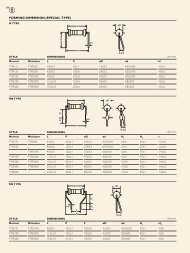
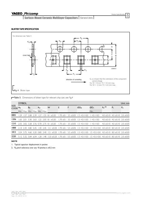
Surface-Mount Ceramic Multilayer CapacitorsGeneral dataProduct specification416BLISTER TAPE SPECIFICATIONFor dimension see Table 4K 0D 0P 2P 0Ecover tapeFWB0A 0D 1SCM015T 2P 1direction of unreelingK 0 : so chosen that the orientation of the componentcannot changeFor W = 8 mm: T2 = 3.5 mm max.For W = 12 mm: T2 = 6.5 mm max.Fig. 4 Blister tapeTable 5 Dimensions of blister tape for relevant chip size; see Fig.4SYMBOLSIZECODE A 0 B 0 K 0 W E F ØD 0 ØD 1(2)P 0Min. Max. Min. Max. Min. Max.Min.P 1 P 2Unit: mm0805 1.29 1.57 2.08 2.39 1.27 1.55 8.1 ±0.20 1.70 ±0.1 3.5 ±0.05 1.5 +0.1/-0.0 1 +0.1/-0.0 4.0 ±0.10 4.0 ±0.10 2.0 ±0.051206 1.65 2.01 3.30 3.63 1.22 2.03 8.1 ±0.20 1.70 ±0.1 3.5 ±0.05 1.5 +0.1/-0.0 1 +0.1/-0.0 4.0 ±0.10 4.0 ±0.10 2.0 ±0.051210 2.55 3.02 3.28 3.76 0.78 2.75 8.1 ±0.20 1.70 ±0.1 3.5 ±0.05 1.5 +0.1/-0.0 1 +0.1/-0.0 4.0 ±0.10 4.0 ±0.10 2.0 ±0.051808 2.10 2.45 4.80 5.45 1.30 2.45 12.1 ±0.20 1.70 ±0.1 5.5 ±0.05 1.5 +0.1/-0.0 1.5 +0.1/-0.0 4.0 ±0.10 8.0 ±0.10 2.0 ±0.051812 3.24 3.75 4.60 5.20 0.80 2.40 12.1 ±0.20 1.70 ±0.1 5.5 ±0.05 1.5 +0.1/-0.0 1.5 +0.1/-0.0 4.0 ±0.10 8.0 ±0.10 2.0 ±0.052220 5.12 5.32 5.84 6.04 1.28 1.48 12.0 ±0.20 1.70 ±0.1 5.5 ±0.05 1.5 +0.1/-0.0 1.5 +0.1/-0.0 4.0 ±0.10 8.0 ±0.10 2.0 ±0.05NOTE1. Typical capacitor displacement in pocket2. P 0 pitch tolerance over any 10 pitches is ±0.2 mmSep 15, 2010 V.13www.yageo.com