MOC'08, Trends and Technology SMILE and WLC - SUSS MicroTec
MOC'08, Trends and Technology SMILE and WLC - SUSS MicroTec
MOC'08, Trends and Technology SMILE and WLC - SUSS MicroTec

Create successful ePaper yourself
Turn your PDF publications into a flip-book with our unique Google optimized e-Paper software.
Templates ‘08 p.1/4<br />
TECHNOLOGY TRENDS OF MICROLENS IMPRINT LITHOGRAPHY<br />
AND WAFER LEVEL CAMERAS (<strong>WLC</strong>)<br />
Reinhard Voelkel (1) , Jacques Duparre (2) , Frank Wippermann (2) , Peter Dannberg (2) , Andreas Bräuer (2) , Ralph Zoberbier (3) , Markus<br />
Gabriel (3) , Michael Hornung (3) , Sven Hansen (3) , Ralf Suess (3)<br />
(1) <strong>SUSS</strong> MicroOptics SA, Jaquet-Droz 7, CH-2000 Neuchâtel, Switzerl<strong>and</strong>, +41-32-7205104, voelkel@suss.ch, www.suss.ch<br />
(2) Fraunhofer-Institut für Angew. Optik und Feinmechanik IOF, Albert-Einstein-Str. 7, 07745 Jena, Germany, www.microoptics.org<br />
(3) Suss <strong>MicroTec</strong> Lithography GmbH, Schleissheimerstrasse 80, D-85748 Garching, Germany, www.suss.com<br />
Abstract: Wafer Level Cameras (<strong>WLC</strong>) are a novel technology to manufacture low-cost CMOS cameras for mobile phones. The<br />
optical components are fabricated on glass wafers by microlens imprint lithography using a <strong>SUSS</strong> <strong>MicroTec</strong> mask aligner. Opto-<br />
Wafers <strong>and</strong> the CMOS-Wafer are mounted by Wafer-Level Packaging (WLP). A technology overview <strong>and</strong> recent trends will be<br />
presented.<br />
© 2008 Microoptics Group (OSJ/JSAP)<br />
1. Introduction<br />
In 1994, about 20 years after the invention of the digital<br />
still camera <strong>and</strong> 10 years after first mobile phones<br />
appeared on the market, the first digital consumer<br />
camera, the “Apple Quick Take”, was introduced to the<br />
market. It took another 8 years until digital cameras were<br />
integrated into mobile phones. In the beginning, a mobile<br />
phone camera was just another gimmick with limited<br />
value for the mobile phone user. Memory was expensive,<br />
<strong>and</strong> the image quality was poor. Today, it is difficult to<br />
find a mobile phone without digital camera. Most mobile<br />
phones are now equipped with two cameras, a primary<br />
Mega-Pixel (MP) camera for photography <strong>and</strong> a<br />
secondary CIF or VGA camera for video calls. Far more<br />
than a billion mobile phone cameras were sold in 2007,<br />
<strong>and</strong> the numbers are still increasing rapidly.<br />
2. <strong>Trends</strong> for Mobile Phone Cameras<br />
It is difficult to predict long term developments in the<br />
field of mobile phone technology. Regarding mobile<br />
phone cameras, the situation is much easier, they will get<br />
better, they will get cheaper – but they remain to be an<br />
indispensable part of a mobile phone. Today, two main<br />
trends are observed:<br />
a) High resolution cameras, providing autofocus, optical<br />
zoom, mechanical shutter, stabilization <strong>and</strong> Xenon flash.<br />
Mobile phones equipped with high resolution cameras<br />
are in direct competition with digital still cameras.<br />
b) Wafer-Level Cameras, providing a high potential for<br />
cost-reduction in the low end camera market. The<br />
camera should be “reflowable”, i.e. it must survive<br />
st<strong>and</strong>ard SMT reflow soldering process at about 260°C.<br />
Both trends will certainly have a tremendous impact on<br />
the current optics <strong>and</strong> digital camera industry.<br />
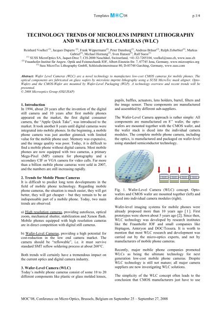
3. Wafer-Level Camera (<strong>WLC</strong>)<br />
Today’s mobile phone cameras consist of some 10 to 20<br />
different components like plastic or glass molded lenses,<br />
pupils, baffles, actuators, lens holders, barrel, filters <strong>and</strong><br />
the image sensor. These components are manufactured<br />
<strong>and</strong> assembled by different sub-suppliers.<br />
The Wafer-Level Camera approach is rather simple: All<br />
components are manufactured on 8’’ wafer, the optowafers<br />
are mounted together with the CMOS wafer, <strong>and</strong><br />
the wafer stack is diced into the individual camera<br />
modules. The complete mobile phone camera, including<br />
the optics, is manufactured <strong>and</strong> packaged on wafer-level<br />
using st<strong>and</strong>ard semiconductor technology.<br />
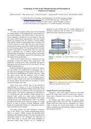
Fig. 1. Wafer-Level Camera (<strong>WLC</strong>) concept. Optowafers<br />
<strong>and</strong> CMOS wafer are mounted together (left) <strong>and</strong><br />
diced into individual camera modules (right).<br />
Wafer-level imaging systems for mobile phones were<br />
already proposed more than 10 years ago [ 1 ]. First<br />
prototypes were shown about 5 years ago [2]. Since then,<br />
<strong>WLC</strong> technology was developed by research institutes<br />
like the Fraunhofer IOF <strong>and</strong> small companies like<br />
Heptagon, Anteryon <strong>and</strong> DOC/Tessera. It is worth to<br />
mention that most <strong>WLC</strong> research <strong>and</strong> development was<br />
carried out by the micro-optics experts, <strong>and</strong> not by<br />
manufacturers of mobile phone cameras.<br />
Recently, major mobile phone companies promoted<br />
<strong>WLC</strong>s as being the ultimate technology for next<br />
generation low-cost mobile phone cameras. Despite<br />
<strong>WLC</strong> technology is still not mature; all major camera<br />
suppliers are now investigating <strong>WLC</strong> solutions.<br />
The simplicity of the <strong>WLC</strong> concept often leads to the<br />
conclusion that CMOS manufacturers just have to use<br />
MOC’08, Conference on Micro-Optics, Brussels, Belgium on September 25 – September 27, 2008
their highly developed semiconductor technology to<br />
manufacture the 8’’ opto-wafers.<br />
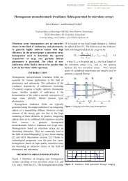
Stop<br />
Polymer-Microlenses<br />
4.3 mm<br />
Silica<br />
Dielectric IR cut-off filter<br />
Templates ‘08 p.2/4<br />
CMOS-imager<br />
Fig.2. Wafer-Level Camera built in WALORI EU-IST<br />
Project [1]. Backside illumination through thinned<br />
CMOS image sensor <strong>and</strong> ball grid for bonding.<br />
Compared to the 150 different process steps to manufacture<br />
a CMOS imager, the opto-wafers with some bulky<br />
lenses should be rather simple to do. In semiconductor<br />
industry “everything is possible” <strong>and</strong> further miniaturization<br />
is only a question of time. However, these assumptions<br />
are not valid for wafer-level optics:<br />
• St<strong>and</strong>ard semiconductor technology is not suitable<br />
for the manufacturing of bi-convex aspherical<br />
lenses on 8’’ wafer level.<br />
• Well established materials from semiconductor<br />
industry can’t be used for wafer optics.<br />
• Most materials used for plastic optics do not<br />
survive reflow processes at 260°C.<br />
• In <strong>WLC</strong> the CMOS sensor is covered by the<br />
glass opto-wafers. Electric contact pads have to<br />
be place on the backside of the CMOS chip <strong>and</strong><br />
Through Silicon Via (TSV) technology or backside<br />
thinning of the CMOS are required.<br />
• Fundamental physical laws limit a scaling down<br />
to ultra small cameras with high resolution.<br />
The <strong>WLC</strong> approach requires a close co-operation of<br />
optics <strong>and</strong> semiconductor industry with equipment<br />
suppliers. Novel technology has to be developed <strong>and</strong><br />
existing production tools have to be modified.<br />
4. Microlens Imprint Lithography<br />
8’’ wafer technology for refractive <strong>and</strong> diffractive microoptics<br />
was first implemented by <strong>SUSS</strong> MicroOptics in<br />
1999. St<strong>and</strong>ard manufacturing technology from semiconductor<br />
industry, like resist coating, lithography,<br />
reactive ion etching (RIE), deposition, sputtering, <strong>and</strong><br />
lift-off were optimized to manufacture high-quality<br />
micro-optics in 8’’ Fused Silica, Silicon <strong>and</strong> Borofloat<br />
wafers. Unfortunately, the well-established 8’’ wafer<br />
technology is not suitable for <strong>WLC</strong>. Resist melting <strong>and</strong><br />
RIE transfer do not allow manufacturing of microlenses<br />
with more than 100 µm lens sag. RIE speed of some<br />
MOC’08, Conference on Micro-Optics, Brussels, Belgium on September 25 – September 27, 2008<br />
4.5 mm<br />
microns per minute does not allow cost-efficient etching<br />
of bi-convex lenses on wafer level.<br />
The most promising technology is imprinting or UVembossing<br />
of polymer lens structures on glass wafers by<br />
soft PDMS stamps. First experiments to imprint microoptics<br />
on wafer level using a modified <strong>SUSS</strong> Mask<br />
Aligner MA6 have been carried out at the CSEM about<br />
10 years ago. [3, 4]<br />
Fig. 3. UV-embossed micro-optics using a <strong>SUSS</strong> Mask<br />
Aligner. Sol-gel microlenses for collimation are<br />
imprinted on top of VCSELs (photos CSEM Zurich).<br />
CSEM’s microlens imprint technology has been<br />
transferred to Heptagon, also based in the Zurich area in<br />
Switzerl<strong>and</strong>. Heptagon developed proprietary processes<br />
for reflowable micro-optics <strong>and</strong> is regarded as one of the<br />
pioneers in <strong>WLC</strong> technology. Recently Heptagon opened<br />
a <strong>WLC</strong> manufacturing facility in Singapore. Another<br />
pioneer in this field is the Fraunhofer IOF in Jena,<br />
Germany. They successfully developed replication <strong>and</strong><br />
imprint technologies for low-cost wafer-level optics.<br />
Fully operable prototypes of ultra-flat cameras, endoscopes<br />
cameras <strong>and</strong> <strong>WLC</strong> systems have been presented.<br />
Microlens Imprint Lithography allows the manufacturing<br />
of lens arrays with a lateral accuracy of ± 1 µm on 8’’<br />
wafer level.<br />
mask holder<br />
polymer Polymer resin resin Substrate Mask holder<br />
substrate<br />
Alignment alignment marks marks<br />
mould<br />
WEC enables<br />
precise gap ±1µm<br />
WEC, exposure gap<br />
chuck<br />
Mold<br />
Chuck<br />
back side<br />
microscope<br />
BSA, back side<br />
microscope<br />
Fig. 4. Microlens Imprint Lithography using a soft mold<br />
to imprint double-sided lens arrays onto opto-wafers.<br />
However, Microlens Imprint Lithography is not a<br />
technology that could be easily <strong>and</strong> fast integrated into a
semiconductor manufacturing process. Major problems<br />
are the lack of suitable polymer materials <strong>and</strong> the<br />
availability of wafer-scale master arrays.<br />
The <strong>WLC</strong> lens material must be suitable for high<br />
throughput imprint lithography, reflowable at 260°C <strong>and</strong><br />
must have long-time stability in harsh environment (heat,<br />
humidity <strong>and</strong> sunlight). For the lens design, a choice of<br />
different lens materials (refractive index, Abbé number)<br />
is required. Today, the commercially available materials<br />
do not fulfill these conditions. Companies have developed<br />
their own material, but do not share information.<br />
Fig. 5. (Left) Lens master composed by single diamondturned<br />
pins. (Right) 8’’ lens master obtained by diamond<br />
turning. (Photos Fresnel Optics, Kaleido <strong>Technology</strong>).<br />
Usually, smaller master arrays are used to build a larger<br />
lens master in a step-<strong>and</strong>-repeat procedure on <strong>SUSS</strong> NPS<br />
300 Nano-Imprint-Stepper. Recently Kaleido <strong>Technology</strong><br />
presented a first 8’’ diamond turned lens master in<br />
brass, providing spherical, aspherical <strong>and</strong> free-form<br />
lenses with better than 2 µm lateral position accuracy.<br />
The wafer-scale master arrays are then transferred into a<br />
soft stamp, usually made of Polydimethylsiloxane<br />
(PDMS) by casting. The PDMS layer serves as stamp.<br />
5. Wafer-Level Packaging for Opto-Wafers<br />
<strong>SUSS</strong> MicroOptics, a spin-off from IMT Neuchâtel,<br />
Switzerl<strong>and</strong>, <strong>and</strong> the Institute of Applied Optics<br />
Erlangen, Germany, started the manufacturing of highquality<br />
micro-optics on 8’’ wafer level in 1999.<br />
Fig. 6. <strong>SUSS</strong> Mask Aligner modified for wafer-level<br />
packaging of 8’’ microlens wafers. A stack of 4 microlens<br />
wafers (4’’) serving as a 1:1 array imaging system.<br />
Templates ‘08 p.3/4<br />
At the beginning, the focus was on Microlens Projection<br />
Lithography (MPL), a novel technology using an ultraflat<br />
microlens-based projection systems consisting of 4<br />
wafers (Fused Silica) of densely packed microlens arrays,<br />
pupil <strong>and</strong> baffle arrays.[5] Wafer-level packaging was<br />
done in a modified <strong>SUSS</strong> MA8/BA6 Mask Aligner<br />
providing active gap setting, stiff wafer holders, UV<br />
curing <strong>and</strong> wafer-to-wafer accuracy of ±1 µm.<br />
<strong>SUSS</strong> <strong>MicroTec</strong> has now launched a new mask aligner<br />
dedicated for <strong>WLC</strong>. The new MA8 combines all three<br />
non-semiconductor technologies required for <strong>WLC</strong>:<br />
• Stamp manufacturing<br />
• <strong>SUSS</strong> Microlens Imprint Lithography (<strong>SMILE</strong>)<br />
• Wafer Level Packaging of 8‘‘ opto-wafers<br />
In production, the MA8 Mask Aligner is combined with<br />
a <strong>SUSS</strong> DSM8 or DSM200 for double-side imprint <strong>and</strong><br />
wafer-to-wafer alignment accuracy testing.<br />
Fig. 7. <strong>SUSS</strong> Mask Aligner MA8 dedicated for Wafer-<br />
Level Camera (<strong>WLC</strong>) development <strong>and</strong> production.<br />
<strong>SUSS</strong> DSM8 for testing the alignment accuracy of<br />
double-sided Opto-wafers <strong>and</strong> mounted <strong>WLC</strong> stacks.<br />
Today, the equipment base for <strong>WLC</strong> production is still<br />
very narrow. However, in the case that the <strong>WLC</strong><br />
approach fulfills the very high expectations of the mobile<br />
phone industry, other equipment manufacturers will<br />
quickly follow <strong>and</strong> also provide equipment for <strong>WLC</strong>.<br />
6. Summary<br />
As result of quite a few years of research <strong>and</strong> development,<br />
executed by research institutes <strong>and</strong> small microoptics<br />
companies, first Wafer-Level Cameras get on the<br />
market now. The proof of principle was successful.<br />
However, the <strong>WLC</strong> technology is not yet mature <strong>and</strong> a<br />
fast ramp-up of the camera industry to <strong>WLC</strong> manufacturing<br />
is not very likely. The most critical problems <strong>and</strong><br />
potential show-stoppers are the following:<br />
OPTICAL DESIGN<br />
• Wafer-Level Cameras require novel strategies for<br />
optical design <strong>and</strong> straylight management. Only a<br />
few optical designers have already <strong>WLC</strong> experience.<br />
• Integration of actuators for mechanical zoom or<br />
shutters is difficult or impossible.<br />
MOC’08, Conference on Micro-Optics, Brussels, Belgium on September 25 – September 27, 2008
• The CMOS packing density must be adapted to the<br />
packing density of the opto-wafers. Thus the number<br />
of CMOS chips per wafer might decrease.<br />
LENS MATERIAL<br />
• The lens material must be suitable for highthroughput<br />
imprint lithography, UV-curable, reflowable<br />
at 260°C <strong>and</strong> must have a long-time stability<br />
in harsh environment (heat, humidity <strong>and</strong> sunlight).<br />
• For chromatic correction different lens materials<br />
(crown <strong>and</strong> flint glass type) must be available.<br />
MICROLENS IMPRINT LITHOGRAPHY<br />
• Current Microlens Imprint Lithography suffers from<br />
long process cycles, short stamp lifetime, wafer<br />
bending (bow, warp) <strong>and</strong> significant yield problems.<br />
METROLOGY<br />
• Optical testing of aspherical <strong>and</strong> free-form microlenses<br />
is difficult <strong>and</strong> sometimes impossible.<br />
• High-throughput lens testing on wafer-level is<br />
m<strong>and</strong>atory to maintain a high yield in production.<br />
WAFER-LEVEL PACKAGING<br />
• Opto-wafers are usually not perfectly planar. Bow,<br />
warp <strong>and</strong> double-sided optics make it difficult to<br />
mount a stack of 3-4 different wafers.<br />
• Gluing <strong>and</strong> sealing for the wafer stack is not trivial<br />
regarding reflow temperature restrictions.<br />
• Dicing of the complete <strong>WLC</strong> stack is tricky <strong>and</strong> has<br />
a high impact on the overall yield.<br />
LEGAL ASPECTS<br />
• <strong>WLC</strong> technology is protected by many patents. TSV<br />
(Through Silica Via) technology is also m<strong>and</strong>atory<br />
for <strong>WLC</strong>. The patent situation for these two key<br />
technologies might not be clarified soon.<br />
• The profit margins for mobile phone camera<br />
suppliers are already very tight. <strong>WLC</strong> manufacturers<br />
might simply not earn enough to finance the new<br />
technology <strong>and</strong> to pay the license fees.<br />
7. Outlook<br />
The big players in the mobile phone <strong>and</strong> imager industry<br />
are getting excited about <strong>WLC</strong>s. Driven by harsh costreduction<br />
dem<strong>and</strong>s; all major players are currently<br />
Templates ‘08 p.4/4<br />
evaluating plans to quickly ramp-up <strong>WLC</strong> manufacturing.<br />
Several scenarios are feasible:<br />
A) Today’s <strong>WLC</strong> players, small micro-optics companies<br />
that have successfully developed <strong>WLC</strong> technology, will<br />
grow fast <strong>and</strong> take over the low-end camera market.<br />
B) Today’s phone camera manufacturers will upgrade<br />
from single lens mounting to wafer-level technology.<br />
C) Semiconductor industry will implement <strong>WLC</strong><br />
technology in their CMOS lines. Current camera<br />
suppliers will be pushed out of the supply chain.<br />
Very likely, none of these scenarios will happen like<br />
this. Today’s <strong>WLC</strong> players might not be able to ramp-up<br />
fast enough. They will try to find partners to sell their<br />
technology or IP. Today’s camera manufacturers will<br />
have a hard time to change from single lens molding to<br />
8’’ wafer technology. They will try to find other<br />
solutions to reduce their costs without major changes.<br />
Semiconductor industry underestimates the challenge of<br />
lens manufacturing. The most likely scenario is a mix<br />
<strong>and</strong> match of different technologies <strong>and</strong> strategies:<br />
• Both molded plastic <strong>and</strong> glass lenses <strong>and</strong> 8’’ wafers<br />
of imprinted lens structures will be used together.<br />
• Die-to-wafer, reconstitute wafer or carrier integration<br />
strategies as shown in Figure 8.<br />
Fig. 8. <strong>WLC</strong> concept using separation <strong>and</strong> carrier wafers<br />
as proposed by A*Star, Singapore.<br />
Acknowledgement<br />
The presented work is co-financed by the BMBF VDI<br />
research project COMIKA.<br />
[1] R. Völkel, S. Wallstab, Flachbauendes Bilderfassungssystem“ Patent DE 19917890 A1 (1999).<br />
[2] EU-IST-2001-35366, Project WALORI, WAfer Level Optic solution foR compact CMOS Imager (2002-2005).<br />
[3] M.T. Gale, “Replication,” Chapter 6 in Micro-Optics: Elements, Systems <strong>and</strong> Applications, H.P. Herzig, Ed., Taylor <strong>and</strong> Francis,<br />
London (1997).<br />
[4] Brite-Euram Project BE97-464 1, DONDODEM, Development of new dielectric <strong>and</strong> optical materials <strong>and</strong> process-technologies<br />
for low cost electrical <strong>and</strong>/or optical packaging <strong>and</strong> testing of precompetitive demonstrators, (1998-2001).<br />
[5] R. Völkel, H.P. Herzig, Ph. Nussbaum, W. Singer, K.J. Weible, R. Dändliker, W.B. Hugle, Microlens lithography: a new<br />
fabrication Method for very large displays, Asia Display'95, pp. 713-716, 1995.<br />
MOC’08, Conference on Micro-Optics, Brussels, Belgium on September 25 – September 27, 2008