Schottky Barrier Diode Video Detectors Application Note 923
Schottky Barrier Diode Video Detectors Application Note 923
Schottky Barrier Diode Video Detectors Application Note 923

Create successful ePaper yourself
Turn your PDF publications into a flip-book with our unique Google optimized e-Paper software.
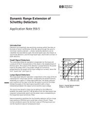
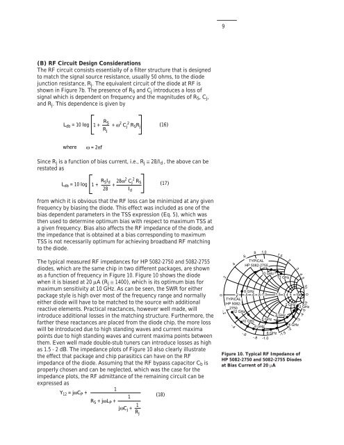
9(B) RF Circuit Design ConsiderationsThe RF circuit consists essentially of a filter structure that is designedto match the signal source resistance, usually 50 ohms, to the diodejunction resistance, R j . The equivalent circuit of the diode at RF isshown in Figure 7b. The presence of R S and C j introduces a loss ofsignal which is dependent on frequency and the magnitudes of R S , C j ,and R j . This dependence is given byL + ω 2 C 2 db = 10 log 1 + R Sj R S R j (16)R jwhereω = 2πfSince R j is a function of bias current, i.e., R j ≅ 28/I d , the above can berestated as28ω 2 C 2 j RL Sdb = 10 log 1 + R SI d+28 I d(17)from which it is obvious that the RF loss can be minimized at any givenfrequency by biasing the diode. This effect was included as one of thebias dependent parameters in the TSS expression (Eq. 5), which wasthen used to determine optimum bias with respect to maximum TSS ata given frequency. Bias also affects the RF impedance of the diode, andthe impedance that is obtained at a bias corresponding to maximumTSS is not necessarily optimum for achieving broadband RF matchingto the diode.The typical measured RF impedances for HP 5082-2750 and 5082-2755diodes, which are the same chip in two different packages, are shownas a function of frequency in Figure 10. Figure 10 shows the diodewhen it is biased at 20 µA (R j ≅ 1400), which is its optimum bias formaximum sensitivity at 10 GHz. As can be seen, the SWR for eitherpackage style is high over most of the frequency range and normallyeither diode will have to be matched to the source with additionalreactive elements. Practical reactances, however well made, willintroduce additional losses in the matching structure. Furthermore, thefarther these reactances are placed from the diode chip, the more losswill be introduced due to high standing waves and current maximapoints due to high standing waves and current maxima points betweenthem. Even well made double-stub tuners can introduce losses as highas 1.5 - 2 dB. The impedance plots of Figure 10 also clearly illustratethe effect that package and chip parasitics can have on the RFimpedance of the diode. Assuming that the RF bypass capacitor C b isproperly chosen and can be neglected, which was the case for theimpedance plots, the RF admittance of the remaining circuit can beexpressed as1Y 12 = jωC P +1(18)R S + jωL P +1jωC j +R j0.2-.2.4.6.81.01.58 GHz.2 .4 .6 .8 1.0 1.5 3 4 5 10TYPICALHP 5082-27502 GHz 2 GHz12 GHz4 GHz10 GHz6 GHz8 GHz4 GHz6 GHz-.4-.6TYPICALHP 5082-2755-.810 GHz-1.0-1.5212 GHz-23-34510-10-5-4Figure 10. Typical RF Impedance ofHP 5082-2750 and 5082-2755 <strong>Diode</strong>sat Bias Current of 20 µA0